
Advanced Configuration and Power
Interface (ACPI) Specification
Release 6.5
UEFI Forum, Inc.
Aug 29, 2022

CONTENTS
1 Introduction 1
1.1 Principal Goals . . . . . . . . . . . . . . . . . . . . . . . . . . . . . . . . . . . . . . . . . . . . . . 1
1.1.1 Principle of Inclusive Terminology . . . . . . . . . . . . . . . . . . . . . . . . . . . . . . . 2
1.2 Power Management Rationale . . . . . . . . . . . . . . . . . . . . . . . . . . . . . . . . . . . . . . 2
1.3 Legacy Support . . . . . . . . . . . . . . . . . . . . . . . . . . . . . . . . . . . . . . . . . . . . . . 3
1.4 OEM Implementation Strategy . . . . . . . . . . . . . . . . . . . . . . . . . . . . . . . . . . . . . . 4
1.5 Power and Sleep Buttons . . . . . . . . . . . . . . . . . . . . . . . . . . . . . . . . . . . . . . . . . 4
1.6 ACPI Specification and the Structure of ACPI . . . . . . . . . . . . . . . . . . . . . . . . . . . . . . 4
1.7 OS and Platform Compliance . . . . . . . . . . . . . . . . . . . . . . . . . . . . . . . . . . . . . . 6
1.7.1 Platform Implementations of ACPI-defined Interfaces . . . . . . . . . . . . . . . . . . . . . 6
1.7.1.1 Recommended Features and Interface Descriptions for Design Guides . . . . . . . 6
1.7.1.2 Terminology Examples for Design Guides . . . . . . . . . . . . . . . . . . . . . . 8
1.7.2 OSPM Implementations . . . . . . . . . . . . . . . . . . . . . . . . . . . . . . . . . . . . 10
1.7.3 OS Requirements . . . . . . . . . . . . . . . . . . . . . . . . . . . . . . . . . . . . . . . . 11
1.8 Target Audience . . . . . . . . . . . . . . . . . . . . . . . . . . . . . . . . . . . . . . . . . . . . . 11
1.9 Document Organization . . . . . . . . . . . . . . . . . . . . . . . . . . . . . . . . . . . . . . . . . 12
1.9.1 ACPI Introduction and Overview . . . . . . . . . . . . . . . . . . . . . . . . . . . . . . . . 12
1.9.2 Programming Models . . . . . . . . . . . . . . . . . . . . . . . . . . . . . . . . . . . . . . 12
1.9.3 Implementation Details . . . . . . . . . . . . . . . . . . . . . . . . . . . . . . . . . . . . . 13
1.9.4 Technical Reference . . . . . . . . . . . . . . . . . . . . . . . . . . . . . . . . . . . . . . 13
1.9.5 Revsion Numbers . . . . . . . . . . . . . . . . . . . . . . . . . . . . . . . . . . . . . . . . 14
1.10 Related Documents . . . . . . . . . . . . . . . . . . . . . . . . . . . . . . . . . . . . . . . . . . . . 14
2 Definition of Terms 15
2.1 General ACPI Terminology . . . . . . . . . . . . . . . . . . . . . . . . . . . . . . . . . . . . . . . 15
2.2 Global System State Definitions . . . . . . . . . . . . . . . . . . . . . . . . . . . . . . . . . . . . . 21
2.3 Device Power State Definitions . . . . . . . . . . . . . . . . . . . . . . . . . . . . . . . . . . . . . 23
2.3.1 Device Performance States . . . . . . . . . . . . . . . . . . . . . . . . . . . . . . . . . . . 24
2.4 Sleeping and Soft-off State Definitions . . . . . . . . . . . . . . . . . . . . . . . . . . . . . . . . . 24
2.5 Processor Power State Definitions . . . . . . . . . . . . . . . . . . . . . . . . . . . . . . . . . . . . 25
2.6 Device and Processor Performance State Definitions . . . . . . . . . . . . . . . . . . . . . . . . . . 25
3 ACPI Concepts 26
3.1 System Power Management . . . . . . . . . . . . . . . . . . . . . . . . . . . . . . . . . . . . . . . 27
3.2 Power States . . . . . . . . . . . . . . . . . . . . . . . . . . . . . . . . . . . . . . . . . . . . . . . 27
3.2.1 Power Button . . . . . . . . . . . . . . . . . . . . . . . . . . . . . . . . . . . . . . . . . . 28
3.2.2 Platform Power Management Characteristics . . . . . . . . . . . . . . . . . . . . . . . . . 29
3.2.2.1 Mobile PC . . . . . . . . . . . . . . . . . . . . . . . . . . . . . . . . . . . . . . . 29
3.2.2.2 Desktop PCs . . . . . . . . . . . . . . . . . . . . . . . . . . . . . . . . . . . . . . 29
3.2.2.3 Multiprocessor and Server PCs . . . . . . . . . . . . . . . . . . . . . . . . . . . . 29
i

3.3 Device Power Management . . . . . . . . . . . . . . . . . . . . . . . . . . . . . . . . . . . . . . . 30
3.3.1 Device Power Management Model . . . . . . . . . . . . . . . . . . . . . . . . . . . . . . . 30
3.3.2 Power Management Standards . . . . . . . . . . . . . . . . . . . . . . . . . . . . . . . . . 31
3.3.3 Device Power States . . . . . . . . . . . . . . . . . . . . . . . . . . . . . . . . . . . . . . 31
3.3.4 Device Power State Definitions . . . . . . . . . . . . . . . . . . . . . . . . . . . . . . . . . 31
3.4 Controlling Device Power . . . . . . . . . . . . . . . . . . . . . . . . . . . . . . . . . . . . . . . . 32
3.4.1 Getting Device Power Capabilities . . . . . . . . . . . . . . . . . . . . . . . . . . . . . . . 32
3.4.2 Setting Device Power States . . . . . . . . . . . . . . . . . . . . . . . . . . . . . . . . . . 32
3.4.3 Getting Device Power Status . . . . . . . . . . . . . . . . . . . . . . . . . . . . . . . . . . 33
3.4.4 Waking the System . . . . . . . . . . . . . . . . . . . . . . . . . . . . . . . . . . . . . . . 33
3.4.5 Example: Modem Device Power Management . . . . . . . . . . . . . . . . . . . . . . . . . 34
3.4.5.1 Obtaining the Modem Capabilities . . . . . . . . . . . . . . . . . . . . . . . . . . 35
3.4.5.2 Setting the Modem Power State . . . . . . . . . . . . . . . . . . . . . . . . . . . . 35
3.4.5.3 Obtaining the Modem Power Status . . . . . . . . . . . . . . . . . . . . . . . . . . 35
3.4.5.4 Waking the System . . . . . . . . . . . . . . . . . . . . . . . . . . . . . . . . . . 36
3.5 Processor Power Management . . . . . . . . . . . . . . . . . . . . . . . . . . . . . . . . . . . . . . 36
3.6 Device and Processor Performance States . . . . . . . . . . . . . . . . . . . . . . . . . . . . . . . . 36
3.7 Configuration and “Plug and Play” . . . . . . . . . . . . . . . . . . . . . . . . . . . . . . . . . . . 37
3.7.1 Device Configuration Example: Configuring the Modem . . . . . . . . . . . . . . . . . . . 37
3.7.2 NUMA Nodes . . . . . . . . . . . . . . . . . . . . . . . . . . . . . . . . . . . . . . . . . . 37
3.8 System Events . . . . . . . . . . . . . . . . . . . . . . . . . . . . . . . . . . . . . . . . . . . . . . 37
3.9 Battery Management . . . . . . . . . . . . . . . . . . . . . . . . . . . . . . . . . . . . . . . . . . . 38
3.9.1 Battery Communications . . . . . . . . . . . . . . . . . . . . . . . . . . . . . . . . . . . . 38
3.9.2 Battery Capacity . . . . . . . . . . . . . . . . . . . . . . . . . . . . . . . . . . . . . . . . 39
3.9.3 Battery Gas Gauge . . . . . . . . . . . . . . . . . . . . . . . . . . . . . . . . . . . . . . . 39
3.9.4 Low Battery Levels . . . . . . . . . . . . . . . . . . . . . . . . . . . . . . . . . . . . . . . 40
3.9.4.1 Emergency Shutdown . . . . . . . . . . . . . . . . . . . . . . . . . . . . . . . . . 41
3.9.5 Battery Calibration . . . . . . . . . . . . . . . . . . . . . . . . . . . . . . . . . . . . . . . 41
3.9.6 Battery Charge Limiting . . . . . . . . . . . . . . . . . . . . . . . . . . . . . . . . . . . . 42
3.10 Thermal Management Concepts . . . . . . . . . . . . . . . . . . . . . . . . . . . . . . . . . . . . . 43
3.10.1 Active and Passive Cooling Modes . . . . . . . . . . . . . . . . . . . . . . . . . . . . . . . 43
3.10.2 Performance vs. Energy Conservation . . . . . . . . . . . . . . . . . . . . . . . . . . . . . 44
3.10.3 Acoustics (Noise) . . . . . . . . . . . . . . . . . . . . . . . . . . . . . . . . . . . . . . . . 44
3.10.4 Multiple Thermal Zones . . . . . . . . . . . . . . . . . . . . . . . . . . . . . . . . . . . . 44
3.11 Flexible Platform Architecture Support . . . . . . . . . . . . . . . . . . . . . . . . . . . . . . . . . 44
3.11.1 Hardware-reduced ACPI . . . . . . . . . . . . . . . . . . . . . . . . . . . . . . . . . . . . 45
3.11.1.1 Interrupt-based Wake Events . . . . . . . . . . . . . . . . . . . . . . . . . . . . . 45
3.11.2 Low-Power Idle . . . . . . . . . . . . . . . . . . . . . . . . . . . . . . . . . . . . . . . . . 45
3.11.2.1 Low Power S0 Idle Capable Flag . . . . . . . . . . . . . . . . . . . . . . . . . . . 45
3.11.3 Connection Resources . . . . . . . . . . . . . . . . . . . . . . . . . . . . . . . . . . . . . 46
3.11.3.1 Supported Platforms . . . . . . . . . . . . . . . . . . . . . . . . . . . . . . . . . . 46
4 ACPI Hardware Specification 48
4.1 Hardware-Reduced ACPI . . . . . . . . . . . . . . . . . . . . . . . . . . . . . . . . . . . . . . . . 48
4.1.1 Hardware-Reduced Events . . . . . . . . . . . . . . . . . . . . . . . . . . . . . . . . . . . 49
4.1.1.1 GPIO-Signaled Events or Interrupt Signaled Events . . . . . . . . . . . . . . . . . 49
4.1.1.2 Interrupt-based Wake Events . . . . . . . . . . . . . . . . . . . . . . . . . . . . . 49
4.2 Fixed Hardware Programming Model . . . . . . . . . . . . . . . . . . . . . . . . . . . . . . . . . . 49
4.3 Generic Hardware Programming Model . . . . . . . . . . . . . . . . . . . . . . . . . . . . . . . . . 50
4.4 Diagram Legend . . . . . . . . . . . . . . . . . . . . . . . . . . . . . . . . . . . . . . . . . . . . . 52
4.5 Register Bit Notation . . . . . . . . . . . . . . . . . . . . . . . . . . . . . . . . . . . . . . . . . . . 52
4.6 The ACPI Hardware Model . . . . . . . . . . . . . . . . . . . . . . . . . . . . . . . . . . . . . . . 53
4.6.1 Hardware Reserved Bits . . . . . . . . . . . . . . . . . . . . . . . . . . . . . . . . . . . . 56
4.6.2 Hardware Ignored Bits . . . . . . . . . . . . . . . . . . . . . . . . . . . . . . . . . . . . . 56
ii

4.6.3 Hardware Write-Only Bits . . . . . . . . . . . . . . . . . . . . . . . . . . . . . . . . . . . 56
4.6.4 Cross Device Dependencies . . . . . . . . . . . . . . . . . . . . . . . . . . . . . . . . . . 57
4.6.4.1 Example 1: Related Device Interference . . . . . . . . . . . . . . . . . . . . . . . 57
4.6.4.2 Example 2: Unrelated Device Interference . . . . . . . . . . . . . . . . . . . . . . 57
4.7 ACPI Hardware Features . . . . . . . . . . . . . . . . . . . . . . . . . . . . . . . . . . . . . . . . . 57
4.8 ACPI Register Model . . . . . . . . . . . . . . . . . . . . . . . . . . . . . . . . . . . . . . . . . . 59
4.8.1 ACPI Register Summary . . . . . . . . . . . . . . . . . . . . . . . . . . . . . . . . . . . . 61
4.8.1.1 PM1 Event Registers . . . . . . . . . . . . . . . . . . . . . . . . . . . . . . . . . 62
4.8.1.2 PM1 Control Registers . . . . . . . . . . . . . . . . . . . . . . . . . . . . . . . . 63
4.8.1.3 PM2 Control Register . . . . . . . . . . . . . . . . . . . . . . . . . . . . . . . . . 63
4.8.1.4 PM Timer Register . . . . . . . . . . . . . . . . . . . . . . . . . . . . . . . . . . 63
4.8.1.5 Processor Control Block (P_BLK) . . . . . . . . . . . . . . . . . . . . . . . . . . 63
4.8.1.6 General-Purpose Event Registers . . . . . . . . . . . . . . . . . . . . . . . . . . . 64
4.8.2 Fixed Hardware Features . . . . . . . . . . . . . . . . . . . . . . . . . . . . . . . . . . . . 64
4.8.2.1 Power Management Timer . . . . . . . . . . . . . . . . . . . . . . . . . . . . . . 64
4.8.2.2 Console Buttons . . . . . . . . . . . . . . . . . . . . . . . . . . . . . . . . . . . . 65
4.8.2.3 Sleeping/Wake Control . . . . . . . . . . . . . . . . . . . . . . . . . . . . . . . . 70
4.8.2.4 Real Time Clock Alarm . . . . . . . . . . . . . . . . . . . . . . . . . . . . . . . . 71
4.8.2.5 Legacy/ACPI Select and the SCI Interrupt . . . . . . . . . . . . . . . . . . . . . . 72
4.8.2.6 Processor Control . . . . . . . . . . . . . . . . . . . . . . . . . . . . . . . . . . . 73
4.8.3 Fixed Hardware Registers . . . . . . . . . . . . . . . . . . . . . . . . . . . . . . . . . . . 74
4.8.3.1 PM1 Event Grouping . . . . . . . . . . . . . . . . . . . . . . . . . . . . . . . . . 74
4.8.3.2 PM1 Control Grouping . . . . . . . . . . . . . . . . . . . . . . . . . . . . . . . . 77
4.8.3.3 Power Management Timer (PM_TMR) . . . . . . . . . . . . . . . . . . . . . . . . 79
4.8.3.4 PM2 Control (PM2_CNT) . . . . . . . . . . . . . . . . . . . . . . . . . . . . . . . 79
4.8.3.5 Processor Register Block (P_BLK) . . . . . . . . . . . . . . . . . . . . . . . . . . 80
4.8.3.6 Reset Register . . . . . . . . . . . . . . . . . . . . . . . . . . . . . . . . . . . . . 81
4.8.3.7 Sleep Control and Status Registers . . . . . . . . . . . . . . . . . . . . . . . . . . 82
4.8.4 Generic Hardware Registers . . . . . . . . . . . . . . . . . . . . . . . . . . . . . . . . . . 83
4.8.4.1 General-Purpose Event Register Blocks . . . . . . . . . . . . . . . . . . . . . . . . 85
4.8.4.2 Example Generic Devices . . . . . . . . . . . . . . . . . . . . . . . . . . . . . . . 87
5 ACPI Software Programming Model 90
5.1 Overview of the System Description Table Architecture . . . . . . . . . . . . . . . . . . . . . . . . 90
5.1.1 Address Space Translation . . . . . . . . . . . . . . . . . . . . . . . . . . . . . . . . . . . 93
5.2 ACPI System Description Tables . . . . . . . . . . . . . . . . . . . . . . . . . . . . . . . . . . . . 93
5.2.1 Reserved Bits and Fields . . . . . . . . . . . . . . . . . . . . . . . . . . . . . . . . . . . . 94
5.2.1.1 Reserved Bits and Software Components . . . . . . . . . . . . . . . . . . . . . . . 94
5.2.1.2 Reserved Values and Software Components . . . . . . . . . . . . . . . . . . . . . 94
5.2.1.3 Reserved Hardware Bits and Software Components . . . . . . . . . . . . . . . . . 94
5.2.1.4 Ignored Hardware Bits and Software Components . . . . . . . . . . . . . . . . . . 95
5.2.2 Compatibility . . . . . . . . . . . . . . . . . . . . . . . . . . . . . . . . . . . . . . . . . . 95
5.2.3 Address Format . . . . . . . . . . . . . . . . . . . . . . . . . . . . . . . . . . . . . . . . . 95
5.2.3.1 Functional Fixed Hardware . . . . . . . . . . . . . . . . . . . . . . . . . . . . . . 95
5.2.3.2 Generic Address Structure . . . . . . . . . . . . . . . . . . . . . . . . . . . . . . . 96
5.2.4 Universally Unique Identifiers (UUIDs) . . . . . . . . . . . . . . . . . . . . . . . . . . . . 98
5.2.5 Root System Description Pointer (RSDP) . . . . . . . . . . . . . . . . . . . . . . . . . . . 98
5.2.5.1 Finding the RSDP on IA-PC Systems . . . . . . . . . . . . . . . . . . . . . . . . . 98
5.2.5.2 Finding the RSDP on UEFI Enabled Systems . . . . . . . . . . . . . . . . . . . . 98
5.2.5.3 Root System Description Pointer (RSDP) Structure . . . . . . . . . . . . . . . . . 99
5.2.6 System Description Table Header . . . . . . . . . . . . . . . . . . . . . . . . . . . . . . . 99
5.2.7 Root System Description Table (RSDT) . . . . . . . . . . . . . . . . . . . . . . . . . . . . 104
5.2.8 Extended System Description Table (XSDT) . . . . . . . . . . . . . . . . . . . . . . . . . . 104
5.2.9 Fixed ACPI Description Table (FADT) . . . . . . . . . . . . . . . . . . . . . . . . . . . . . 105
iii

5.2.9.1 Preferred PM Profile System Types . . . . . . . . . . . . . . . . . . . . . . . . . . 118
5.2.9.2 System Type Attributes . . . . . . . . . . . . . . . . . . . . . . . . . . . . . . . . 119
5.2.9.3 IA-PC Boot Architecture Flags . . . . . . . . . . . . . . . . . . . . . . . . . . . . 119
5.2.9.4 ARM Architecture Boot Flags . . . . . . . . . . . . . . . . . . . . . . . . . . . . . 120
5.2.10 Firmware ACPI Control Structure (FACS) . . . . . . . . . . . . . . . . . . . . . . . . . . . 121
5.2.10.1 Global Lock . . . . . . . . . . . . . . . . . . . . . . . . . . . . . . . . . . . . . . 123
5.2.11 Definition Blocks . . . . . . . . . . . . . . . . . . . . . . . . . . . . . . . . . . . . . . . . 125
5.2.11.1 Differentiated System Description Table (DSDT) . . . . . . . . . . . . . . . . . . 126
5.2.11.2 Secondary System Description Table (SSDT) . . . . . . . . . . . . . . . . . . . . . 126
5.2.11.3 Persistent System Description Table (PSDT) . . . . . . . . . . . . . . . . . . . . . 127
5.2.12 Multiple APIC Description Table (MADT) . . . . . . . . . . . . . . . . . . . . . . . . . . 127
5.2.12.1 MADT Processor Local APIC / SAPIC Structure Entry Order . . . . . . . . . . . . 130
5.2.12.2 Processor Local APIC Structure . . . . . . . . . . . . . . . . . . . . . . . . . . . . 130
5.2.12.3 I/O APIC Structure . . . . . . . . . . . . . . . . . . . . . . . . . . . . . . . . . . 131
5.2.12.4 Platforms with APIC and Dual 8259 Support . . . . . . . . . . . . . . . . . . . . . 131
5.2.12.5 Interrupt Source Override Structure . . . . . . . . . . . . . . . . . . . . . . . . . . 132
5.2.12.6 Non-Maskable Interrupt (NMI) Source Structure . . . . . . . . . . . . . . . . . . . 133
5.2.12.7 Local APIC NMI Structure . . . . . . . . . . . . . . . . . . . . . . . . . . . . . . 133
5.2.12.8 Local APIC Address Override Structure . . . . . . . . . . . . . . . . . . . . . . . 134
5.2.12.9 I/O SAPIC Structure . . . . . . . . . . . . . . . . . . . . . . . . . . . . . . . . . . 134
5.2.12.10 Local SAPIC Structure . . . . . . . . . . . . . . . . . . . . . . . . . . . . . . . . 135
5.2.12.11 Platform Interrupt Source Structure . . . . . . . . . . . . . . . . . . . . . . . . . . 135
5.2.12.12 Processor Local x2APIC Structure . . . . . . . . . . . . . . . . . . . . . . . . . . 137
5.2.12.13 Local x2APIC NMI Structure . . . . . . . . . . . . . . . . . . . . . . . . . . . . . 137
5.2.12.14 GIC CPU Interface (GICC) Structure . . . . . . . . . . . . . . . . . . . . . . . . . 138
5.2.12.15 GIC Distributor (GICD) Structure . . . . . . . . . . . . . . . . . . . . . . . . . . . 140
5.2.12.16 GIC MSI Frame Structure . . . . . . . . . . . . . . . . . . . . . . . . . . . . . . . 141
5.2.12.17 GIC Redistributor (GICR) Structure . . . . . . . . . . . . . . . . . . . . . . . . . 142
5.2.12.18 GIC Interrupt Translation Service (ITS) Structure . . . . . . . . . . . . . . . . . . 142
5.2.12.19 Multiprocessor Wakeup Structure . . . . . . . . . . . . . . . . . . . . . . . . . . . 142
5.2.12.20 Core Programmable Interrupt Controller (CORE PIC) Structure . . . . . . . . . . . 144
5.2.12.21 Legacy I/O Programmable Interrupt Controller(LIO PIC) Structure . . . . . . . . . 145
5.2.12.22 HyperTransport Programmable Interrupt Controller (HT PIC) Structure . . . . . . . 145
5.2.12.23 Extend I/O Programmable Interrupt Controller (EIO PIC) Structure . . . . . . . . . 146
5.2.12.24 MSI Programmable Interrupt Controller (MSI PIC) Structure . . . . . . . . . . . . 146
5.2.12.25 Bridge I/O Programmable Interrupt Controller (BIO PIC) Structure . . . . . . . . . 147
5.2.12.26 LPC Programmable Interrupt Controller (LPC PIC) Structure . . . . . . . . . . . . 147
5.2.13 Global System Interrupts . . . . . . . . . . . . . . . . . . . . . . . . . . . . . . . . . . . . 148
5.2.14 Smart Battery Table (SBST) . . . . . . . . . . . . . . . . . . . . . . . . . . . . . . . . . . 150
5.2.15 Embedded Controller Boot Resources Table (ECDT) . . . . . . . . . . . . . . . . . . . . . 151
5.2.16 System Resource Affinity Table (SRAT) . . . . . . . . . . . . . . . . . . . . . . . . . . . . 153
5.2.16.1 Processor Local APIC/SAPIC Affinity Structure . . . . . . . . . . . . . . . . . . . 154
5.2.16.2 Memory Affinity Structure . . . . . . . . . . . . . . . . . . . . . . . . . . . . . . 154
5.2.16.3 Processor Local x2APIC Affinity Structure . . . . . . . . . . . . . . . . . . . . . . 155
5.2.16.4 GICC Affinity Structure . . . . . . . . . . . . . . . . . . . . . . . . . . . . . . . . 156
5.2.16.5 GIC Interrupt Translation Service (ITS) Affinity Structure . . . . . . . . . . . . . . 156
5.2.16.6 Generic Initiator Affinity Structure . . . . . . . . . . . . . . . . . . . . . . . . . . 157
5.2.16.7 Generic Port Affinity Structure . . . . . . . . . . . . . . . . . . . . . . . . . . . . 158
5.2.17 System Locality Information Table (SLIT) . . . . . . . . . . . . . . . . . . . . . . . . . . . 159
5.2.18 Corrected Platform Error Polling Table (CPEP) . . . . . . . . . . . . . . . . . . . . . . . . 160
5.2.18.1 Corrected Platform Error Polling Processor Structure . . . . . . . . . . . . . . . . 161
5.2.19 Maximum System Characteristics Table (MSCT) . . . . . . . . . . . . . . . . . . . . . . . 162
5.2.19.1 Maximum Proximity Domain Information Structure . . . . . . . . . . . . . . . . . 163
5.2.20 ACPI RAS Feature Table (RASF) . . . . . . . . . . . . . . . . . . . . . . . . . . . . . . . 164
iv

5.2.20.1 RASF PCC Sub Channel Identifier . . . . . . . . . . . . . . . . . . . . . . . . . . 165
5.2.20.2 Using PCC registers . . . . . . . . . . . . . . . . . . . . . . . . . . . . . . . . . . 165
5.2.20.3 RASF Communication Channel . . . . . . . . . . . . . . . . . . . . . . . . . . . . 165
5.2.20.4 Platform RAS Capabilities . . . . . . . . . . . . . . . . . . . . . . . . . . . . . . 166
5.2.20.5 Parameter Block . . . . . . . . . . . . . . . . . . . . . . . . . . . . . . . . . . . . 167
5.2.21 ACPI RAS2 Feature Table (RAS2) . . . . . . . . . . . . . . . . . . . . . . . . . . . . . . . 168
5.2.21.1 Common Definitions . . . . . . . . . . . . . . . . . . . . . . . . . . . . . . . . . 169
5.2.21.2 Memory RAS Features – Feature Type 0 . . . . . . . . . . . . . . . . . . . . . . . 171
5.2.22 Memory Power State Table (MPST) . . . . . . . . . . . . . . . . . . . . . . . . . . . . . . 175
5.2.22.1 MPST PCC Sub Channel . . . . . . . . . . . . . . . . . . . . . . . . . . . . . . . 177
5.2.22.2 Memory Power State . . . . . . . . . . . . . . . . . . . . . . . . . . . . . . . . . 180
5.2.22.3 Action Sequence . . . . . . . . . . . . . . . . . . . . . . . . . . . . . . . . . . . . 181
5.2.22.4 Memory Power Node . . . . . . . . . . . . . . . . . . . . . . . . . . . . . . . . . 182
5.2.22.5 Memory Power State Structure . . . . . . . . . . . . . . . . . . . . . . . . . . . . 184
5.2.22.6 Memory Power State Characteristics structure . . . . . . . . . . . . . . . . . . . . 184
5.2.22.7 Autonomous Memory Power Management . . . . . . . . . . . . . . . . . . . . . . 185
5.2.22.8 Handling BIOS Reserved Memory . . . . . . . . . . . . . . . . . . . . . . . . . . 186
5.2.22.9 Interaction with NUMA processor and memory affinity tables . . . . . . . . . . . . 186
5.2.22.10 Interaction with Memory Hot Plug . . . . . . . . . . . . . . . . . . . . . . . . . . 186
5.2.22.11 OS Memory Allocation Considerations . . . . . . . . . . . . . . . . . . . . . . . . 187
5.2.22.12 Platform Memory Topology Table (PMTT) . . . . . . . . . . . . . . . . . . . . . . 187
5.2.23 Boot Graphics Resource Table (BGRT) . . . . . . . . . . . . . . . . . . . . . . . . . . . . 190
5.2.23.1 Version . . . . . . . . . . . . . . . . . . . . . . . . . . . . . . . . . . . . . . . . . 192
5.2.23.2 Status . . . . . . . . . . . . . . . . . . . . . . . . . . . . . . . . . . . . . . . . . 192
5.2.23.3 Image Type . . . . . . . . . . . . . . . . . . . . . . . . . . . . . . . . . . . . . . 192
5.2.23.4 Image Address . . . . . . . . . . . . . . . . . . . . . . . . . . . . . . . . . . . . . 192
5.2.23.5 Image Offset . . . . . . . . . . . . . . . . . . . . . . . . . . . . . . . . . . . . . . 192
5.2.24 Firmware Performance Data Table (FPDT) . . . . . . . . . . . . . . . . . . . . . . . . . . 193
5.2.24.1 Performance Record Format . . . . . . . . . . . . . . . . . . . . . . . . . . . . . . 194
5.2.24.2 FPDT Performance Record Types . . . . . . . . . . . . . . . . . . . . . . . . . . . 195
5.2.24.3 Runtime Performance Record Types . . . . . . . . . . . . . . . . . . . . . . . . . 195
5.2.24.4 Firmware Basic Boot Performance Table Pointer Record . . . . . . . . . . . . . . . 195
5.2.24.5 S3 Performance Table Pointer Record . . . . . . . . . . . . . . . . . . . . . . . . . 196
5.2.24.6 Firmware Basic Boot Performance Table . . . . . . . . . . . . . . . . . . . . . . . 196
5.2.24.7 Firmware Basic Boot Performance Data Record . . . . . . . . . . . . . . . . . . . 197
5.2.24.8 S3 Performance Table . . . . . . . . . . . . . . . . . . . . . . . . . . . . . . . . . 197
5.2.25 Generic Timer Description Table (GTDT) . . . . . . . . . . . . . . . . . . . . . . . . . . . 198
5.2.25.1 GT Block Structure . . . . . . . . . . . . . . . . . . . . . . . . . . . . . . . . . . 201
5.2.25.2 Arm Generic Watchdog Structure . . . . . . . . . . . . . . . . . . . . . . . . . . . 203
5.2.26 NVDIMM Firmware Interface Table (NFIT) . . . . . . . . . . . . . . . . . . . . . . . . . . 204
5.2.26.1 Overview . . . . . . . . . . . . . . . . . . . . . . . . . . . . . . . . . . . . . . . 204
5.2.26.2 System Physical Address (SPA) Range Structure . . . . . . . . . . . . . . . . . . . 206
5.2.26.3 NVDIMM Region Mapping Structure . . . . . . . . . . . . . . . . . . . . . . . . 208
5.2.26.4 Interleave Structure . . . . . . . . . . . . . . . . . . . . . . . . . . . . . . . . . . 211
5.2.26.5 SMBIOS Management Information Structure . . . . . . . . . . . . . . . . . . . . . 212
5.2.26.6 NVDIMM Control Region Structure . . . . . . . . . . . . . . . . . . . . . . . . . 212
5.2.26.7 NVDIMM Block Data Window Region Structure . . . . . . . . . . . . . . . . . . 215
5.2.26.8 Flush Hint Address Structure . . . . . . . . . . . . . . . . . . . . . . . . . . . . . 215
5.2.26.9 Platform Capabilities Structure . . . . . . . . . . . . . . . . . . . . . . . . . . . . 216
5.2.26.10 NVDIMM Representation Format . . . . . . . . . . . . . . . . . . . . . . . . . . 217
5.2.27 Secure Devices (SDEV) ACPI Table . . . . . . . . . . . . . . . . . . . . . . . . . . . . . . 218
5.2.27.1 Secure Device Structures . . . . . . . . . . . . . . . . . . . . . . . . . . . . . . . 219
5.2.28 Heterogeneous Memory Attribute Table (HMAT) . . . . . . . . . . . . . . . . . . . . . . . 223
5.2.28.1 HMAT Overview . . . . . . . . . . . . . . . . . . . . . . . . . . . . . . . . . . . 223
v

5.2.28.2 Memory Side Cache Overview . . . . . . . . . . . . . . . . . . . . . . . . . . . . 224
5.2.28.3 Memory Proximity Domain Attributes Structure . . . . . . . . . . . . . . . . . . . 224
5.2.28.4 System Locality Latency and Bandwidth Information Structure . . . . . . . . . . . 225
5.2.28.5 Memory Side Cache Information Structure . . . . . . . . . . . . . . . . . . . . . . 229
5.2.29 Platform Debug Trigger Table (PDTT) . . . . . . . . . . . . . . . . . . . . . . . . . . . . . 231
5.2.29.1 PDTT PCC Sub Channel . . . . . . . . . . . . . . . . . . . . . . . . . . . . . . . 232
5.2.29.2 PDTT PCC Trigger Order . . . . . . . . . . . . . . . . . . . . . . . . . . . . . . . 234
5.2.29.3 Example: OS Invoking Multiple Debug Triggers . . . . . . . . . . . . . . . . . . . 234
5.2.30 Processor Properties Topology Table (PPTT) . . . . . . . . . . . . . . . . . . . . . . . . . 236
5.2.30.1 Processor hierarchy node structure (Type 0) . . . . . . . . . . . . . . . . . . . . . 237
5.2.30.2 Cache Type Structure - Type 1 . . . . . . . . . . . . . . . . . . . . . . . . . . . . 239
5.2.31 Platform Health Assessment Table (PHAT) . . . . . . . . . . . . . . . . . . . . . . . . . . 243
5.2.31.1 Platform Health Assessment Record Format . . . . . . . . . . . . . . . . . . . . . 243
5.2.31.2 Platform Health Assessment Record Type Format . . . . . . . . . . . . . . . . . . 244
5.2.31.3 Firmware Version Data Record Structure . . . . . . . . . . . . . . . . . . . . . . . 244
5.2.31.4 Firmware Health Data Record Structure . . . . . . . . . . . . . . . . . . . . . . . 245
5.2.31.5 Reset Reason Health Record . . . . . . . . . . . . . . . . . . . . . . . . . . . . . 246
5.2.32 Virtual I/O Translation (VIOT) Table . . . . . . . . . . . . . . . . . . . . . . . . . . . . . . 250
5.2.32.1 Virtual I/O Translation (VIOT) Table Header . . . . . . . . . . . . . . . . . . . . . 251
5.2.32.2 VIOT Node Structures . . . . . . . . . . . . . . . . . . . . . . . . . . . . . . . . . 251
5.2.32.3 PCI Range Node Structure . . . . . . . . . . . . . . . . . . . . . . . . . . . . . . 252
5.2.32.4 Single MMIO Endpoint Node Structure . . . . . . . . . . . . . . . . . . . . . . . . 252
5.2.32.5 virtio-iommu based on virtio-pci Node Structure . . . . . . . . . . . . . . . . . . . 253
5.2.32.6 virtio-iommu based on virtio-mmioNode Structure . . . . . . . . . . . . . . . . . . 253
5.2.33 Miscellaneous GUIDed Table Entries . . . . . . . . . . . . . . . . . . . . . . . . . . . . . 253
5.2.34 CC Event Log ACPI Table . . . . . . . . . . . . . . . . . . . . . . . . . . . . . . . . . . . 254
5.2.35 Storage Volume Key Location Table . . . . . . . . . . . . . . . . . . . . . . . . . . . . . . 255
5.3 ACPI Namespace . . . . . . . . . . . . . . . . . . . . . . . . . . . . . . . . . . . . . . . . . . . . . 256
5.3.1 Predefined Root Namespaces . . . . . . . . . . . . . . . . . . . . . . . . . . . . . . . . . . 258
5.3.2 Objects . . . . . . . . . . . . . . . . . . . . . . . . . . . . . . . . . . . . . . . . . . . . . 258
5.4 Definition Block Encoding . . . . . . . . . . . . . . . . . . . . . . . . . . . . . . . . . . . . . . . . 259
5.4.1 AML Encoding . . . . . . . . . . . . . . . . . . . . . . . . . . . . . . . . . . . . . . . . . 259
5.4.2 Definition Block Loading . . . . . . . . . . . . . . . . . . . . . . . . . . . . . . . . . . . . 259
5.5 Control Methods and the ACPI Source Language (ASL) . . . . . . . . . . . . . . . . . . . . . . . . 261
5.5.1 ASL Statements . . . . . . . . . . . . . . . . . . . . . . . . . . . . . . . . . . . . . . . . . 262
5.5.2 Control Method Execution . . . . . . . . . . . . . . . . . . . . . . . . . . . . . . . . . . . 262
5.5.2.1 Arguments . . . . . . . . . . . . . . . . . . . . . . . . . . . . . . . . . . . . . . . 262
5.5.2.2 Method Calling Convention . . . . . . . . . . . . . . . . . . . . . . . . . . . . . . 263
5.5.2.3 Local Variables and Locally Created Data Objects . . . . . . . . . . . . . . . . . . 263
5.5.2.4 Access to Operation Regions . . . . . . . . . . . . . . . . . . . . . . . . . . . . . 264
5.6 ACPI Event Programming Model . . . . . . . . . . . . . . . . . . . . . . . . . . . . . . . . . . . . 290
5.6.1 ACPI Event Programming Model Components . . . . . . . . . . . . . . . . . . . . . . . . 290
5.6.2 Types of ACPI Events . . . . . . . . . . . . . . . . . . . . . . . . . . . . . . . . . . . . . . 291
5.6.3 Fixed Event Handling . . . . . . . . . . . . . . . . . . . . . . . . . . . . . . . . . . . . . . 291
5.6.4 General-Purpose Event Handling . . . . . . . . . . . . . . . . . . . . . . . . . . . . . . . . 292
5.6.4.1 _Exx, _Lxx, and _Qxx Methods for GPE Processing . . . . . . . . . . . . . . . . . 293
5.6.4.2 GPE Wake Events . . . . . . . . . . . . . . . . . . . . . . . . . . . . . . . . . . . 294
5.6.5 GPIO-signaled ACPI Events . . . . . . . . . . . . . . . . . . . . . . . . . . . . . . . . . . 296
5.6.5.1 Declaring GPIO Controller Devices . . . . . . . . . . . . . . . . . . . . . . . . . . 296
5.6.5.2 _AEI Object for GPIO-signaled Events . . . . . . . . . . . . . . . . . . . . . . . . 296
5.6.5.3 The Event (_EVT) Method for Handling GPIO-signaled Events . . . . . . . . . . . 297
5.6.6 Device Object Notifications . . . . . . . . . . . . . . . . . . . . . . . . . . . . . . . . . . . 298
5.6.7 Device Class-Specific Objects . . . . . . . . . . . . . . . . . . . . . . . . . . . . . . . . . 303
5.6.8 Predefined ACPI Names for Objects, Methods, and Resources . . . . . . . . . . . . . . . . 305
vi

5.6.9 Interrupt-signaled ACPI events . . . . . . . . . . . . . . . . . . . . . . . . . . . . . . . . . 312
5.6.9.1 Declaring Generic Event Device . . . . . . . . . . . . . . . . . . . . . . . . . . . 312
5.6.9.2 _CRS Object for Interrupt-signaled Events . . . . . . . . . . . . . . . . . . . . . . 312
5.6.9.3 The Event (_EVT) Method for Handling Interrupt-signaled Events . . . . . . . . . 313
5.6.9.4 GED Wake Events . . . . . . . . . . . . . . . . . . . . . . . . . . . . . . . . . . . 314
5.6.10 Managing a Wake Event Using Device _PRW Objects . . . . . . . . . . . . . . . . . . . . 315
5.7 Predefined Objects . . . . . . . . . . . . . . . . . . . . . . . . . . . . . . . . . . . . . . . . . . . . 315
5.7.1 \_GL (Global Lock Mutex) . . . . . . . . . . . . . . . . . . . . . . . . . . . . . . . . . . . 315
5.7.2 \_OSI (Operating System Interfaces) . . . . . . . . . . . . . . . . . . . . . . . . . . . . . . 315
5.7.2.1 _OSI Examples . . . . . . . . . . . . . . . . . . . . . . . . . . . . . . . . . . . . 317
5.7.3 \_OS (OS Name Object) . . . . . . . . . . . . . . . . . . . . . . . . . . . . . . . . . . . . 318
5.7.4 \_REV (Revision Data Object) . . . . . . . . . . . . . . . . . . . . . . . . . . . . . . . . . 319
5.7.5 \_DLM (DeviceLock Mutex) . . . . . . . . . . . . . . . . . . . . . . . . . . . . . . . . . . 319
5.8 System Configuration Objects . . . . . . . . . . . . . . . . . . . . . . . . . . . . . . . . . . . . . . 321
5.8.1 \_PIC Method . . . . . . . . . . . . . . . . . . . . . . . . . . . . . . . . . . . . . . . . . . 321
6 Device Configuration 322
6.1 Device Identification Objects . . . . . . . . . . . . . . . . . . . . . . . . . . . . . . . . . . . . . . 322
6.1.1 _ADR (Address) . . . . . . . . . . . . . . . . . . . . . . . . . . . . . . . . . . . . . . . . 323
6.1.2 _CID (Compatible ID) . . . . . . . . . . . . . . . . . . . . . . . . . . . . . . . . . . . . . 324
6.1.3 _CLS (Class Code) . . . . . . . . . . . . . . . . . . . . . . . . . . . . . . . . . . . . . . . 325
6.1.4 _DDN (DOS Device Name) . . . . . . . . . . . . . . . . . . . . . . . . . . . . . . . . . . 326
6.1.5 _HID (Hardware ID) . . . . . . . . . . . . . . . . . . . . . . . . . . . . . . . . . . . . . . 326
6.1.6 _HRV (Hardware Revision) . . . . . . . . . . . . . . . . . . . . . . . . . . . . . . . . . . 327
6.1.7 _MLS (Multiple Language String) . . . . . . . . . . . . . . . . . . . . . . . . . . . . . . . 327
6.1.8 _PLD (Physical Location of Device) . . . . . . . . . . . . . . . . . . . . . . . . . . . . . . 328
6.1.9 _SUB (Subsystem ID) . . . . . . . . . . . . . . . . . . . . . . . . . . . . . . . . . . . . . 334
6.1.10 _STR (String) . . . . . . . . . . . . . . . . . . . . . . . . . . . . . . . . . . . . . . . . . . 336
6.1.11 _SUN (Slot User Number) . . . . . . . . . . . . . . . . . . . . . . . . . . . . . . . . . . . 336
6.1.12 _UID (Unique ID) . . . . . . . . . . . . . . . . . . . . . . . . . . . . . . . . . . . . . . . 337
6.2 Device Configuration Objects . . . . . . . . . . . . . . . . . . . . . . . . . . . . . . . . . . . . . . 337
6.2.1 _CDM (Clock Domain) . . . . . . . . . . . . . . . . . . . . . . . . . . . . . . . . . . . . . 338
6.2.2 _CRS (Current Resource Settings) . . . . . . . . . . . . . . . . . . . . . . . . . . . . . . . 339
6.2.3 _DIS (Disable) . . . . . . . . . . . . . . . . . . . . . . . . . . . . . . . . . . . . . . . . . 339
6.2.4 _DMA (Direct Memory Access) . . . . . . . . . . . . . . . . . . . . . . . . . . . . . . . . 339
6.2.5 _DSD (Device Specific Data) . . . . . . . . . . . . . . . . . . . . . . . . . . . . . . . . . . 341
6.2.6 _FIX (Fixed Register Resource Provider) . . . . . . . . . . . . . . . . . . . . . . . . . . . 343
6.2.7 _GSB (Global System Interrupt Base) . . . . . . . . . . . . . . . . . . . . . . . . . . . . . 345
6.2.8 _HPP (Hot Plug Parameters) . . . . . . . . . . . . . . . . . . . . . . . . . . . . . . . . . . 346
6.2.9 _HPX (Hot Plug Parameter Extensions) . . . . . . . . . . . . . . . . . . . . . . . . . . . . 348
6.2.9.1 PCI Setting Record (Type 0) . . . . . . . . . . . . . . . . . . . . . . . . . . . . . 349
6.2.9.2 PCI-X Setting Record (Type 1) . . . . . . . . . . . . . . . . . . . . . . . . . . . . 350
6.2.9.3 PCI Express Setting Record (Type 2) . . . . . . . . . . . . . . . . . . . . . . . . . 350
6.2.9.4 PCI Express Descriptor Setting Record (Type 3) . . . . . . . . . . . . . . . . . . . 352
6.2.9.5 _HPX Example . . . . . . . . . . . . . . . . . . . . . . . . . . . . . . . . . . . . 359
6.2.10 _MAT (Multiple APIC Table Entry) . . . . . . . . . . . . . . . . . . . . . . . . . . . . . . 360
6.2.11 _OSC (Operating System Capabilities) . . . . . . . . . . . . . . . . . . . . . . . . . . . . . 361
6.2.11.1 Rules for Evaluating _OSC . . . . . . . . . . . . . . . . . . . . . . . . . . . . . . 363
6.2.11.2 Platform-Wide OSPM Capabilities . . . . . . . . . . . . . . . . . . . . . . . . . . 364
6.2.11.3 Operating System Capabilities (_OSC) for USB . . . . . . . . . . . . . . . . . . . 366
6.2.12 _PRS (Possible Resource Settings) . . . . . . . . . . . . . . . . . . . . . . . . . . . . . . . 367
6.2.13 _PRT (PCI Routing Table) . . . . . . . . . . . . . . . . . . . . . . . . . . . . . . . . . . . 367
6.2.13.1 Example: Using _PRT to Describe PCI IRQ Routing . . . . . . . . . . . . . . . . . 368
6.2.14 _PXM (Proximity) . . . . . . . . . . . . . . . . . . . . . . . . . . . . . . . . . . . . . . . 369
vii

6.2.15 _SLI (System Locality Information) . . . . . . . . . . . . . . . . . . . . . . . . . . . . . . 370
6.2.16 _SRS (Set Resource Settings) . . . . . . . . . . . . . . . . . . . . . . . . . . . . . . . . . 373
6.2.17 _CCA (Cache Coherency Attribute) . . . . . . . . . . . . . . . . . . . . . . . . . . . . . . 373
6.2.17.1 _CCA Example ASL: . . . . . . . . . . . . . . . . . . . . . . . . . . . . . . . . . 374
6.2.18 _HMA(Heterogeneous Memory Attributes) . . . . . . . . . . . . . . . . . . . . . . . . . . 375
6.3 Device Insertion, Removal, and Status Objects . . . . . . . . . . . . . . . . . . . . . . . . . . . . . 376
6.3.1 _EDL (Eject Device List) . . . . . . . . . . . . . . . . . . . . . . . . . . . . . . . . . . . . 377
6.3.2 _EJD (Ejection Dependent Device) . . . . . . . . . . . . . . . . . . . . . . . . . . . . . . . 378
6.3.3 _EJx (Eject) . . . . . . . . . . . . . . . . . . . . . . . . . . . . . . . . . . . . . . . . . . . 379
6.3.4 _LCK (Lock) . . . . . . . . . . . . . . . . . . . . . . . . . . . . . . . . . . . . . . . . . . 380
6.3.5 _OST (OSPM Status Indication) . . . . . . . . . . . . . . . . . . . . . . . . . . . . . . . . 380
6.3.5.1 Processing Sequence for Graceful Shutdown Request: . . . . . . . . . . . . . . . . 381
6.3.5.2 Processing Sequence for Error Disconnect Recover . . . . . . . . . . . . . . . . . 385
6.3.6 _RMV (Remove) . . . . . . . . . . . . . . . . . . . . . . . . . . . . . . . . . . . . . . . . 385
6.3.7 _STA (Device Status) . . . . . . . . . . . . . . . . . . . . . . . . . . . . . . . . . . . . . . 386
6.4 Resource Data Types for ACPI . . . . . . . . . . . . . . . . . . . . . . . . . . . . . . . . . . . . . . 387
6.4.1 ASL Macros for Resource Descriptors . . . . . . . . . . . . . . . . . . . . . . . . . . . . . 387
6.4.2 Small Resource Data Type . . . . . . . . . . . . . . . . . . . . . . . . . . . . . . . . . . . 387
6.4.2.1 IRQ Descriptor . . . . . . . . . . . . . . . . . . . . . . . . . . . . . . . . . . . . 387
6.4.2.2 DMA Descriptor . . . . . . . . . . . . . . . . . . . . . . . . . . . . . . . . . . . . 388
6.4.2.3 Start Dependent Functions Descriptor . . . . . . . . . . . . . . . . . . . . . . . . . 389
6.4.2.4 End Dependent Functions Descriptor . . . . . . . . . . . . . . . . . . . . . . . . . 390
6.4.2.5 I/O Port Descriptor . . . . . . . . . . . . . . . . . . . . . . . . . . . . . . . . . . 390
6.4.2.6 Fixed Location I/O Port Descriptor . . . . . . . . . . . . . . . . . . . . . . . . . . 391
6.4.2.7 Fixed DMA Descriptor . . . . . . . . . . . . . . . . . . . . . . . . . . . . . . . . 392
6.4.2.8 Vendor-Defined Descriptor, Type 0 . . . . . . . . . . . . . . . . . . . . . . . . . . 392
6.4.2.9 End Tag . . . . . . . . . . . . . . . . . . . . . . . . . . . . . . . . . . . . . . . . 392
6.4.3 Large Resource Data Type . . . . . . . . . . . . . . . . . . . . . . . . . . . . . . . . . . . 393
6.4.3.1 24-Bit Memory Range Descriptor . . . . . . . . . . . . . . . . . . . . . . . . . . . 394
6.4.3.2 Vendor-Defined Descriptor, Type 1 . . . . . . . . . . . . . . . . . . . . . . . . . . 395
6.4.3.3 32-Bit Memory Range Descriptor . . . . . . . . . . . . . . . . . . . . . . . . . . . 395
6.4.3.4 32-Bit Fixed Memory Range Descriptor . . . . . . . . . . . . . . . . . . . . . . . 397
6.4.3.5 Address Space Resource Descriptors . . . . . . . . . . . . . . . . . . . . . . . . . 398
6.4.3.6 Extended Interrupt Descriptor . . . . . . . . . . . . . . . . . . . . . . . . . . . . . 410
6.4.3.7 Generic Register Descriptor . . . . . . . . . . . . . . . . . . . . . . . . . . . . . . 412
6.4.3.8 Connection Descriptors . . . . . . . . . . . . . . . . . . . . . . . . . . . . . . . . 413
6.4.3.9 Pin Function Descriptor . . . . . . . . . . . . . . . . . . . . . . . . . . . . . . . . 424
6.4.3.10 Pin Configuration Descriptor . . . . . . . . . . . . . . . . . . . . . . . . . . . . . 425
6.4.3.11 Pin Group Descriptor . . . . . . . . . . . . . . . . . . . . . . . . . . . . . . . . . 427
6.4.3.12 Pin Group Function Descriptor . . . . . . . . . . . . . . . . . . . . . . . . . . . . 429
6.4.3.13 Pin Group Configuration Descriptor . . . . . . . . . . . . . . . . . . . . . . . . . 430
6.4.3.14 Clock Input Resource Descriptor . . . . . . . . . . . . . . . . . . . . . . . . . . . 432
6.5 Other Objects and Control Methods . . . . . . . . . . . . . . . . . . . . . . . . . . . . . . . . . . . 433
6.5.1 _INI (Init) . . . . . . . . . . . . . . . . . . . . . . . . . . . . . . . . . . . . . . . . . . . . 434
6.5.2 _DCK (Dock) . . . . . . . . . . . . . . . . . . . . . . . . . . . . . . . . . . . . . . . . . . 434
6.5.3 _BDN (BIOS Dock Name) . . . . . . . . . . . . . . . . . . . . . . . . . . . . . . . . . . . 435
6.5.4 _REG (Region) . . . . . . . . . . . . . . . . . . . . . . . . . . . . . . . . . . . . . . . . . 435
6.5.5 _BBN (Base Bus Number) . . . . . . . . . . . . . . . . . . . . . . . . . . . . . . . . . . . 437
6.5.6 _SEG (Segment) . . . . . . . . . . . . . . . . . . . . . . . . . . . . . . . . . . . . . . . . 437
6.5.7 _GLK (Global Lock) . . . . . . . . . . . . . . . . . . . . . . . . . . . . . . . . . . . . . . 439
6.5.8 _DEP (Operation Region Dependencies) . . . . . . . . . . . . . . . . . . . . . . . . . . . . 439
6.5.9 _FIT (Firmware Interface Table) . . . . . . . . . . . . . . . . . . . . . . . . . . . . . . . . 440
6.5.10 NVDIMM Label Methods . . . . . . . . . . . . . . . . . . . . . . . . . . . . . . . . . . . 441
6.5.10.1 _LSI (Label Storage Information) . . . . . . . . . . . . . . . . . . . . . . . . . . . 441
viii

6.5.10.2 _LSR (Label Storage Read) . . . . . . . . . . . . . . . . . . . . . . . . . . . . . . 442
6.5.10.3 _LSW (Label Storage Write) . . . . . . . . . . . . . . . . . . . . . . . . . . . . . 442
6.5.11 _CBR (CXL Host Bridge Register Info) . . . . . . . . . . . . . . . . . . . . . . . . . . . . 443
7 Power and Performance Management 445
7.1 Power Resource Objects and the Power Management Models . . . . . . . . . . . . . . . . . . . . . 445
7.2 Declaring a Power Resource Object . . . . . . . . . . . . . . . . . . . . . . . . . . . . . . . . . . . 447
7.2.1 Defined Methods for a Power Resource . . . . . . . . . . . . . . . . . . . . . . . . . . . . 448
7.2.2 _OFF . . . . . . . . . . . . . . . . . . . . . . . . . . . . . . . . . . . . . . . . . . . . . . 448
7.2.3 _ON . . . . . . . . . . . . . . . . . . . . . . . . . . . . . . . . . . . . . . . . . . . . . . . 449
7.2.4 _STA (Power Resource Status) . . . . . . . . . . . . . . . . . . . . . . . . . . . . . . . . . 449
7.2.5 Passive Power Resources . . . . . . . . . . . . . . . . . . . . . . . . . . . . . . . . . . . . 449
7.3 Device Power Management Objects . . . . . . . . . . . . . . . . . . . . . . . . . . . . . . . . . . . 450
7.3.1 _DSW (Device Sleep Wake) . . . . . . . . . . . . . . . . . . . . . . . . . . . . . . . . . . 451
7.3.2 _PS0 (Power State 0) . . . . . . . . . . . . . . . . . . . . . . . . . . . . . . . . . . . . . . 452
7.3.3 _PS1 (Power State 1) . . . . . . . . . . . . . . . . . . . . . . . . . . . . . . . . . . . . . . 452
7.3.4 _PS2 (Power State 2) . . . . . . . . . . . . . . . . . . . . . . . . . . . . . . . . . . . . . . 452
7.3.5 _PS3 (Power State 3) . . . . . . . . . . . . . . . . . . . . . . . . . . . . . . . . . . . . . . 453
7.3.6 _PSC (Power State Current) . . . . . . . . . . . . . . . . . . . . . . . . . . . . . . . . . . 453
7.3.7 _PSE (Power State for Enumeration) . . . . . . . . . . . . . . . . . . . . . . . . . . . . . . 453
7.3.8 _PR0 (Power Resources for D0) . . . . . . . . . . . . . . . . . . . . . . . . . . . . . . . . 454
7.3.9 _PR1 (Power Resources for D1) . . . . . . . . . . . . . . . . . . . . . . . . . . . . . . . . 454
7.3.10 _PR2 (Power Resources for D2) . . . . . . . . . . . . . . . . . . . . . . . . . . . . . . . . 455
7.3.11 _PR3 (Power Resources for D3hot) . . . . . . . . . . . . . . . . . . . . . . . . . . . . . . 455
7.3.12 _PRE (Power Resources for Enumeration) . . . . . . . . . . . . . . . . . . . . . . . . . . . 456
7.3.13 _PRW (Power Resources for Wake) . . . . . . . . . . . . . . . . . . . . . . . . . . . . . . 456
7.3.14 _PSW (Power State Wake) . . . . . . . . . . . . . . . . . . . . . . . . . . . . . . . . . . . 458
7.3.15 _IRC (In Rush Current) . . . . . . . . . . . . . . . . . . . . . . . . . . . . . . . . . . . . . 458
7.3.16 _S1D (S1 Device State) . . . . . . . . . . . . . . . . . . . . . . . . . . . . . . . . . . . . . 458
7.3.17 _S2D (S2 Device State) . . . . . . . . . . . . . . . . . . . . . . . . . . . . . . . . . . . . . 459
7.3.18 _S3D (S3 Device State) . . . . . . . . . . . . . . . . . . . . . . . . . . . . . . . . . . . . . 460
7.3.19 _S4D (S4 Device State) . . . . . . . . . . . . . . . . . . . . . . . . . . . . . . . . . . . . . 460
7.3.20 _S0W (S0 Device Wake State) . . . . . . . . . . . . . . . . . . . . . . . . . . . . . . . . . 461
7.3.21 _S1W (S1 Device Wake State) . . . . . . . . . . . . . . . . . . . . . . . . . . . . . . . . . 461
7.3.22 _S2W (S2 Device Wake State) . . . . . . . . . . . . . . . . . . . . . . . . . . . . . . . . . 461
7.3.23 _S3W (S3 Device Wake State) . . . . . . . . . . . . . . . . . . . . . . . . . . . . . . . . . 462
7.3.24 _S4W (S4 Device Wake State) . . . . . . . . . . . . . . . . . . . . . . . . . . . . . . . . . 462
7.3.25 _RST (Device Reset) . . . . . . . . . . . . . . . . . . . . . . . . . . . . . . . . . . . . . . 463
7.3.26 _PRR (Power Resource for Reset) . . . . . . . . . . . . . . . . . . . . . . . . . . . . . . . 463
7.3.27 _DSC (Deepest State for Configuration) . . . . . . . . . . . . . . . . . . . . . . . . . . . . 463
7.4 OEM-Supplied System-Level Control Methods . . . . . . . . . . . . . . . . . . . . . . . . . . . . . 464
7.4.1 \_PTS (Prepare To Sleep) . . . . . . . . . . . . . . . . . . . . . . . . . . . . . . . . . . . . 464
7.4.2 \_Sx (System States) . . . . . . . . . . . . . . . . . . . . . . . . . . . . . . . . . . . . . . 465
7.4.2.1 System \_S0 State (Working) . . . . . . . . . . . . . . . . . . . . . . . . . . . . . 467
7.4.2.2 System \_S1 State (Sleeping with Processor Context Maintained) . . . . . . . . . . 467
7.4.2.3 System \_S2 State . . . . . . . . . . . . . . . . . . . . . . . . . . . . . . . . . . . 467
7.4.2.4 System \_S3 State . . . . . . . . . . . . . . . . . . . . . . . . . . . . . . . . . . . 468
7.4.2.5 System \_S4 State . . . . . . . . . . . . . . . . . . . . . . . . . . . . . . . . . . . 468
7.4.2.6 System \_S5 State (Soft Off) . . . . . . . . . . . . . . . . . . . . . . . . . . . . . 469
7.4.3 \_SWS (System Wake Source) . . . . . . . . . . . . . . . . . . . . . . . . . . . . . . . . . 469
7.4.4 \_TTS (Transition To State) . . . . . . . . . . . . . . . . . . . . . . . . . . . . . . . . . . . 470
7.4.5 \_WAK (System Wake) . . . . . . . . . . . . . . . . . . . . . . . . . . . . . . . . . . . . . 470
7.5 OSPM usage of _PTS, _TTS, and _WAK . . . . . . . . . . . . . . . . . . . . . . . . . . . . . . . . 471
ix

8 Processor Configuration and Control 473
8.1 Processor Power States . . . . . . . . . . . . . . . . . . . . . . . . . . . . . . . . . . . . . . . . . . 473
8.1.1 Processor Power State C0 . . . . . . . . . . . . . . . . . . . . . . . . . . . . . . . . . . . . 475
8.1.2 Processor Power State C1 . . . . . . . . . . . . . . . . . . . . . . . . . . . . . . . . . . . . 476
8.1.3 Processor Power State C2 . . . . . . . . . . . . . . . . . . . . . . . . . . . . . . . . . . . . 477
8.1.4 Processor Power State C3 . . . . . . . . . . . . . . . . . . . . . . . . . . . . . . . . . . . . 478
8.1.5 Additional Processor Power States . . . . . . . . . . . . . . . . . . . . . . . . . . . . . . . 478
8.2 Flushing Caches . . . . . . . . . . . . . . . . . . . . . . . . . . . . . . . . . . . . . . . . . . . . . 479
8.3 Power, Performance, and Throttling State Dependencies . . . . . . . . . . . . . . . . . . . . . . . . 479
8.4 Declaring Processors . . . . . . . . . . . . . . . . . . . . . . . . . . . . . . . . . . . . . . . . . . . 480
8.4.1 Processor Power State Control . . . . . . . . . . . . . . . . . . . . . . . . . . . . . . . . . 481
8.4.1.1 _CST (C States) . . . . . . . . . . . . . . . . . . . . . . . . . . . . . . . . . . . . 481
8.4.1.2 _CSD (C-State Dependency) . . . . . . . . . . . . . . . . . . . . . . . . . . . . . 483
8.4.2 Processor Hierarchy . . . . . . . . . . . . . . . . . . . . . . . . . . . . . . . . . . . . . . . 485
8.4.2.1 Processor Container Device . . . . . . . . . . . . . . . . . . . . . . . . . . . . . . 487
8.4.3 Lower Power Idle States . . . . . . . . . . . . . . . . . . . . . . . . . . . . . . . . . . . . 487
8.4.3.1 Hierarchical Idle States . . . . . . . . . . . . . . . . . . . . . . . . . . . . . . . . 488
8.4.3.2 Idle State Coordination . . . . . . . . . . . . . . . . . . . . . . . . . . . . . . . . 489
8.4.3.3 _LPI (Low Power Idle States) . . . . . . . . . . . . . . . . . . . . . . . . . . . . . 494
8.4.3.4 _RDI (Resource Dependencies for Idle) . . . . . . . . . . . . . . . . . . . . . . . 506
8.4.3.5 Compatibility . . . . . . . . . . . . . . . . . . . . . . . . . . . . . . . . . . . . . 509
8.4.4 Processor Throttling Controls . . . . . . . . . . . . . . . . . . . . . . . . . . . . . . . . . . 509
8.4.4.1 _PTC (Processor Throttling Control) . . . . . . . . . . . . . . . . . . . . . . . . . 510
8.4.4.2 _TSS (Throttling Supported States) . . . . . . . . . . . . . . . . . . . . . . . . . . 511
8.4.4.3 _TPC (Throttling Present Capabilities) . . . . . . . . . . . . . . . . . . . . . . . . 512
8.4.4.4 _TSD (T-State Dependency) . . . . . . . . . . . . . . . . . . . . . . . . . . . . . . 513
8.4.4.5 _TDL (T-state Depth Limit) . . . . . . . . . . . . . . . . . . . . . . . . . . . . . . 516
8.4.5 Processor Performance Control . . . . . . . . . . . . . . . . . . . . . . . . . . . . . . . . . 516
8.4.5.1 _PCT (Performance Control) . . . . . . . . . . . . . . . . . . . . . . . . . . . . . 517
8.4.5.2 _PSS (Performance Supported States) . . . . . . . . . . . . . . . . . . . . . . . . 518
8.4.5.3 _PPC (Performance Present Capabilities) . . . . . . . . . . . . . . . . . . . . . . . 519
8.4.5.4 Processor Performance Control Example . . . . . . . . . . . . . . . . . . . . . . . 519
8.4.5.5 _PSD (P-State Dependency) . . . . . . . . . . . . . . . . . . . . . . . . . . . . . . 521
8.4.5.6 _PDL (P-state Depth Limit) . . . . . . . . . . . . . . . . . . . . . . . . . . . . . . 523
8.4.6 Collaborative Processor Performance Control . . . . . . . . . . . . . . . . . . . . . . . . . 523
8.4.6.1 _CPC (Continuous Performance Control) . . . . . . . . . . . . . . . . . . . . . . . 524
8.4.7 _PPE (Polling for Platform Errors) . . . . . . . . . . . . . . . . . . . . . . . . . . . . . . . 540
8.5 Processor Aggregator Device . . . . . . . . . . . . . . . . . . . . . . . . . . . . . . . . . . . . . . 540
8.5.1 Logical Processor Idling . . . . . . . . . . . . . . . . . . . . . . . . . . . . . . . . . . . . 540
8.5.1.1 _PUR (Processor Utilization Request) . . . . . . . . . . . . . . . . . . . . . . . . 540
8.5.2 OSPM _OST Evaluation . . . . . . . . . . . . . . . . . . . . . . . . . . . . . . . . . . . . 541
9 ACPI-Defined Devices and Device-Specific Objects 542
9.1 Device Object Name Collision . . . . . . . . . . . . . . . . . . . . . . . . . . . . . . . . . . . . . . 542
9.1.1 _DSM (Device Specific Method) . . . . . . . . . . . . . . . . . . . . . . . . . . . . . . . . 542
9.2 \_SI System Indicators . . . . . . . . . . . . . . . . . . . . . . . . . . . . . . . . . . . . . . . . . . 545
9.2.1 _SST (System Status) . . . . . . . . . . . . . . . . . . . . . . . . . . . . . . . . . . . . . . 545
9.2.2 _MSG (Message) . . . . . . . . . . . . . . . . . . . . . . . . . . . . . . . . . . . . . . . . 545
9.2.3 _BLT (Battery Level Threshold) . . . . . . . . . . . . . . . . . . . . . . . . . . . . . . . . 546
9.3 Ambient Light Sensor Device . . . . . . . . . . . . . . . . . . . . . . . . . . . . . . . . . . . . . . 546
9.3.1 Overview . . . . . . . . . . . . . . . . . . . . . . . . . . . . . . . . . . . . . . . . . . . . 547
9.3.2 _ALI (Ambient Light Illuminance) . . . . . . . . . . . . . . . . . . . . . . . . . . . . . . . 547
9.3.3 _ALT (Ambient Light Temperature) . . . . . . . . . . . . . . . . . . . . . . . . . . . . . . 548
9.3.4 _ALC (Ambient Light Color Chromaticity) . . . . . . . . . . . . . . . . . . . . . . . . . . 548
x

9.3.5 _ALR (Ambient Light Response) . . . . . . . . . . . . . . . . . . . . . . . . . . . . . . . 548
9.3.6 _ALP (Ambient Light Polling) . . . . . . . . . . . . . . . . . . . . . . . . . . . . . . . . . 552
9.3.7 Ambient Light Sensor Events . . . . . . . . . . . . . . . . . . . . . . . . . . . . . . . . . . 552
9.3.8 Relationship to Backlight Control Methods . . . . . . . . . . . . . . . . . . . . . . . . . . 553
9.4 Control Method Lid Device . . . . . . . . . . . . . . . . . . . . . . . . . . . . . . . . . . . . . . . 553
9.4.1 _LID . . . . . . . . . . . . . . . . . . . . . . . . . . . . . . . . . . . . . . . . . . . . . . 553
9.5 Control Method Power and Sleep Button Devices . . . . . . . . . . . . . . . . . . . . . . . . . . . . 554
9.6 Generic Container Device . . . . . . . . . . . . . . . . . . . . . . . . . . . . . . . . . . . . . . . . 554
9.7 ATA Controller Devices . . . . . . . . . . . . . . . . . . . . . . . . . . . . . . . . . . . . . . . . . 554
9.7.1 Objects for Both ATA and SATA Controllers . . . . . . . . . . . . . . . . . . . . . . . . . . 555
9.7.1.1 _GTF (Get Task File) . . . . . . . . . . . . . . . . . . . . . . . . . . . . . . . . . 555
9.7.2 IDE Controller Device . . . . . . . . . . . . . . . . . . . . . . . . . . . . . . . . . . . . . 556
9.7.2.1 IDE Controller-specific Objects . . . . . . . . . . . . . . . . . . . . . . . . . . . . 557
9.7.3 Serial ATA (SATA) Controller Device . . . . . . . . . . . . . . . . . . . . . . . . . . . . . 558
9.7.3.1 Definitions . . . . . . . . . . . . . . . . . . . . . . . . . . . . . . . . . . . . . . . 558
9.7.3.2 Overview . . . . . . . . . . . . . . . . . . . . . . . . . . . . . . . . . . . . . . . 559
9.7.3.3 SATA controller-specific control methods . . . . . . . . . . . . . . . . . . . . . . . 559
9.8 Floppy Controller Device Objects . . . . . . . . . . . . . . . . . . . . . . . . . . . . . . . . . . . . 560
9.8.1 _FDE (Floppy Disk Enumerate) . . . . . . . . . . . . . . . . . . . . . . . . . . . . . . . . 560
9.8.2 _FDI (Floppy Disk Information) . . . . . . . . . . . . . . . . . . . . . . . . . . . . . . . . 561
9.8.3 _FDM (Floppy Disk Drive Mode) . . . . . . . . . . . . . . . . . . . . . . . . . . . . . . . 562
9.9 GPE Block Device . . . . . . . . . . . . . . . . . . . . . . . . . . . . . . . . . . . . . . . . . . . . 562
9.9.1 Matching Control Methods for Events in a GPE Block Device . . . . . . . . . . . . . . . . 563
9.10 Module Device . . . . . . . . . . . . . . . . . . . . . . . . . . . . . . . . . . . . . . . . . . . . . . 563
9.11 Memory Devices . . . . . . . . . . . . . . . . . . . . . . . . . . . . . . . . . . . . . . . . . . . . . 566
9.11.1 Address Decoding . . . . . . . . . . . . . . . . . . . . . . . . . . . . . . . . . . . . . . . 566
9.11.2 Memory Bandwidth Monitoring and Reporting . . . . . . . . . . . . . . . . . . . . . . . . 566
9.11.2.1 _MBM (Memory Bandwidth Monitoring Data) . . . . . . . . . . . . . . . . . . . . 567
9.11.2.2 _MSM (Memory Set Monitoring) . . . . . . . . . . . . . . . . . . . . . . . . . . . 568
9.11.3 _OSC Definition for Memory Device . . . . . . . . . . . . . . . . . . . . . . . . . . . . . 568
9.11.4 Example: Memory Device . . . . . . . . . . . . . . . . . . . . . . . . . . . . . . . . . . . 569
9.12 _UPC (USB Port Capabilities) . . . . . . . . . . . . . . . . . . . . . . . . . . . . . . . . . . . . . . 569
9.12.1 USB 2.0 Host Controllers and _UPC and _PLD . . . . . . . . . . . . . . . . . . . . . . . . 574
9.12.2 SuperSpeed USB Port and Connector Mapping . . . . . . . . . . . . . . . . . . . . . . . . 576
9.12.3 USB4 Port and USB-C Connector Mapping . . . . . . . . . . . . . . . . . . . . . . . . . . 576
9.13 _PDO (USB Power Data Object) . . . . . . . . . . . . . . . . . . . . . . . . . . . . . . . . . . . . 580
9.14 PC/AT RTC/CMOS Devices . . . . . . . . . . . . . . . . . . . . . . . . . . . . . . . . . . . . . . . 581
9.14.1 PC/AT-compatible RTC/CMOS Devices (PNP0B00) . . . . . . . . . . . . . . . . . . . . . 581
9.14.2 Intel PIIX4-compatible RTC/CMOS Devices (PNP0B01) . . . . . . . . . . . . . . . . . . . 582
9.14.3 Dallas Semiconductor-compatible RTC/CMOS Devices (PNP0B02) . . . . . . . . . . . . . 583
9.15 User Presence Detection Device . . . . . . . . . . . . . . . . . . . . . . . . . . . . . . . . . . . . . 583
9.15.1 _UPD (User Presence Detect) . . . . . . . . . . . . . . . . . . . . . . . . . . . . . . . . . 583
9.15.2 _UPP (User Presence Polling) . . . . . . . . . . . . . . . . . . . . . . . . . . . . . . . . . 584
9.15.3 User Presence Sensor Events . . . . . . . . . . . . . . . . . . . . . . . . . . . . . . . . . . 584
9.16 I/O APIC Device . . . . . . . . . . . . . . . . . . . . . . . . . . . . . . . . . . . . . . . . . . . . . 584
9.17 Time and Alarm Device . . . . . . . . . . . . . . . . . . . . . . . . . . . . . . . . . . . . . . . . . 585
9.17.1 Overview . . . . . . . . . . . . . . . . . . . . . . . . . . . . . . . . . . . . . . . . . . . . 585
9.17.2 _GCP (Get Capability) . . . . . . . . . . . . . . . . . . . . . . . . . . . . . . . . . . . . . 588
9.17.3 _GRT (Get Real Time) . . . . . . . . . . . . . . . . . . . . . . . . . . . . . . . . . . . . . 589
9.17.4 _SRT (Set Real Time) . . . . . . . . . . . . . . . . . . . . . . . . . . . . . . . . . . . . . . 589
9.17.5 _GWS (Get Wake alarm status) . . . . . . . . . . . . . . . . . . . . . . . . . . . . . . . . . 590
9.17.6 _CWS (Clear Wake alarm status) . . . . . . . . . . . . . . . . . . . . . . . . . . . . . . . . 591
9.17.7 _STP (Set Expired Timer Wake Policy) . . . . . . . . . . . . . . . . . . . . . . . . . . . . 591
9.17.8 _STV (Set Timer Value) . . . . . . . . . . . . . . . . . . . . . . . . . . . . . . . . . . . . 592
xi

9.17.9 _TIP (Expired Timer Wake Policy) . . . . . . . . . . . . . . . . . . . . . . . . . . . . . . . 592
9.17.10 _TIV (Timer Values) . . . . . . . . . . . . . . . . . . . . . . . . . . . . . . . . . . . . . . 592
9.17.11 ACPI Wakeup Alarm Events . . . . . . . . . . . . . . . . . . . . . . . . . . . . . . . . . . 593
9.17.12 Relationship to Real Time Clock Alarm . . . . . . . . . . . . . . . . . . . . . . . . . . . . 593
9.17.13 Time and Alarm device as a replacement to the RTC . . . . . . . . . . . . . . . . . . . . . 593
9.17.14 Relationship to UEFI time source . . . . . . . . . . . . . . . . . . . . . . . . . . . . . . . 593
9.17.15 Example ASL code . . . . . . . . . . . . . . . . . . . . . . . . . . . . . . . . . . . . . . . 593
9.18 Generic Buttons Device . . . . . . . . . . . . . . . . . . . . . . . . . . . . . . . . . . . . . . . . . 597
9.18.1 Button Interrupts . . . . . . . . . . . . . . . . . . . . . . . . . . . . . . . . . . . . . . . . 597
9.18.2 Button Usages and Collections . . . . . . . . . . . . . . . . . . . . . . . . . . . . . . . . . 598
9.18.3 Generic Buttons Device Example . . . . . . . . . . . . . . . . . . . . . . . . . . . . . . . . 599
9.19 NVDIMM Devices . . . . . . . . . . . . . . . . . . . . . . . . . . . . . . . . . . . . . . . . . . . . 600
9.19.1 Overview . . . . . . . . . . . . . . . . . . . . . . . . . . . . . . . . . . . . . . . . . . . . 600
9.19.2 NVDIMM Root Device . . . . . . . . . . . . . . . . . . . . . . . . . . . . . . . . . . . . . 600
9.19.3 NVDIMM Device . . . . . . . . . . . . . . . . . . . . . . . . . . . . . . . . . . . . . . . . 601
9.19.4 Example . . . . . . . . . . . . . . . . . . . . . . . . . . . . . . . . . . . . . . . . . . . . . 601
9.19.5 Loading NVDIMM drivers . . . . . . . . . . . . . . . . . . . . . . . . . . . . . . . . . . . 602
9.19.6 Hot Plug Support . . . . . . . . . . . . . . . . . . . . . . . . . . . . . . . . . . . . . . . . 602
9.19.7 NVDIMM Root Device _DSMs . . . . . . . . . . . . . . . . . . . . . . . . . . . . . . . . 604
9.19.7.1 Input Parameters: . . . . . . . . . . . . . . . . . . . . . . . . . . . . . . . . . . . 604
9.19.7.2 Address Range Scrubbing (ARS) Overview . . . . . . . . . . . . . . . . . . . . . 604
9.19.7.3 Address Range Scrub (ARS) Error Injection Overview . . . . . . . . . . . . . . . . 605
9.19.7.4 Function Index 1 - Query ARS Capabilities . . . . . . . . . . . . . . . . . . . . . . 606
9.19.7.5 Function Index 2 - Start ARS . . . . . . . . . . . . . . . . . . . . . . . . . . . . . 608
9.19.7.6 Function Index 3 - Query ARS Status . . . . . . . . . . . . . . . . . . . . . . . . . 609
9.19.7.7 Function Index 4 - Clear Uncorrectable Error . . . . . . . . . . . . . . . . . . . . . 611
9.19.7.8 Function Index 5 - Translate SPA . . . . . . . . . . . . . . . . . . . . . . . . . . . 612
9.19.7.9 Function Index 7 - ARS Error Inject . . . . . . . . . . . . . . . . . . . . . . . . . 614
9.19.7.10 Function Index 8 - ARS Error Inject Clear . . . . . . . . . . . . . . . . . . . . . . 616
9.19.7.11 Function Index 9 - ARS Error Inject Status Query . . . . . . . . . . . . . . . . . . 616
9.19.7.12 Function Index 0xA - Query ARS Error Inject Capabilities . . . . . . . . . . . . . 617
9.19.8 NVDIMM Device Methods . . . . . . . . . . . . . . . . . . . . . . . . . . . . . . . . . . . 618
9.19.8.1 _NCH (Get NVDIMM Current Health Information) . . . . . . . . . . . . . . . . . 619
9.19.8.2 _NBS (Get NVDIMM Boot Status) . . . . . . . . . . . . . . . . . . . . . . . . . . 621
9.19.8.3 _NIC (Get NVDIMM Health Error Injection Capabilities) . . . . . . . . . . . . . . 621
9.19.8.4 _NIH (NVDIMM Inject/Clear Health Errors) . . . . . . . . . . . . . . . . . . . . . 622
9.19.8.5 _NIG (Get NVDIMM Inject Health Error Status) . . . . . . . . . . . . . . . . . . 624
10 Power Source and Power Meter Devices 626
10.1 Smart Battery Subsystems . . . . . . . . . . . . . . . . . . . . . . . . . . . . . . . . . . . . . . . . 626
10.1.1 ACPI Smart Battery Status Change Notification Requirements . . . . . . . . . . . . . . . . 628
10.1.1.1 Smart Battery Charger . . . . . . . . . . . . . . . . . . . . . . . . . . . . . . . . . 628
10.1.1.2 Smart Battery Charger with optional System Manager or Selector . . . . . . . . . . 629
10.1.1.3 Smart Battery System Manager . . . . . . . . . . . . . . . . . . . . . . . . . . . . 629
10.1.1.4 Smart Battery Selector . . . . . . . . . . . . . . . . . . . . . . . . . . . . . . . . . 629
10.1.2 Smart Battery Objects . . . . . . . . . . . . . . . . . . . . . . . . . . . . . . . . . . . . . . 629
10.1.3 _SBS (Smart Battery Subsystem) . . . . . . . . . . . . . . . . . . . . . . . . . . . . . . . . 630
10.1.3.1 Example: Single Smart Battery Subsystem . . . . . . . . . . . . . . . . . . . . . . 630
10.1.3.2 Multiple Smart Battery Subsystem: Example . . . . . . . . . . . . . . . . . . . . . 631
10.2 Control Method Batteries . . . . . . . . . . . . . . . . . . . . . . . . . . . . . . . . . . . . . . . . 633
10.2.1 Battery Events . . . . . . . . . . . . . . . . . . . . . . . . . . . . . . . . . . . . . . . . . 633
10.2.2 Battery Control Methods . . . . . . . . . . . . . . . . . . . . . . . . . . . . . . . . . . . . 634
10.2.2.1 _BCT (Battery Charge Time) . . . . . . . . . . . . . . . . . . . . . . . . . . . . . 635
10.2.2.2 _BIF (Battery Information) . . . . . . . . . . . . . . . . . . . . . . . . . . . . . . 635
xii

10.2.2.3 _BIX (Battery Information Extended) . . . . . . . . . . . . . . . . . . . . . . . . . 637
10.2.2.4 _BMA (Battery Measurement Averaging Interval) . . . . . . . . . . . . . . . . . . 640
10.2.2.5 _BMC (Battery Maintenance Control) . . . . . . . . . . . . . . . . . . . . . . . . 641
10.2.2.6 _BMD (Battery Maintenance Data) . . . . . . . . . . . . . . . . . . . . . . . . . . 642
10.2.2.7 _BMS (Battery Measurement Sampling Time) . . . . . . . . . . . . . . . . . . . . 645
10.2.2.8 _BPC (Battery Power Characteristics) . . . . . . . . . . . . . . . . . . . . . . . . 645
10.2.2.9 _BPS (Battery Power State) . . . . . . . . . . . . . . . . . . . . . . . . . . . . . . 646
10.2.2.10 _BPT (Battery Power Threshold) . . . . . . . . . . . . . . . . . . . . . . . . . . . 647
10.2.2.11 _BST (Battery Status) . . . . . . . . . . . . . . . . . . . . . . . . . . . . . . . . . 648
10.2.2.12 _BTH (Battery Throttle Limit) . . . . . . . . . . . . . . . . . . . . . . . . . . . . 650
10.2.2.13 _BTM (Battery Time) . . . . . . . . . . . . . . . . . . . . . . . . . . . . . . . . . 651
10.2.2.14 _BTP (Battery Trip Point) . . . . . . . . . . . . . . . . . . . . . . . . . . . . . . . 651
10.2.2.15 _OSC Definition for Control Method Battery . . . . . . . . . . . . . . . . . . . . . 652
10.3 AC Adapters and Power Source Objects . . . . . . . . . . . . . . . . . . . . . . . . . . . . . . . . . 652
10.3.1 _PSR (Power Source) . . . . . . . . . . . . . . . . . . . . . . . . . . . . . . . . . . . . . . 653
10.3.2 _PCL (Power Consumer List) . . . . . . . . . . . . . . . . . . . . . . . . . . . . . . . . . 653
10.3.3 _PIF (Power Source Information) . . . . . . . . . . . . . . . . . . . . . . . . . . . . . . . 653
10.3.4 _PRL (Power Source Redundancy List) . . . . . . . . . . . . . . . . . . . . . . . . . . . . 654
10.4 Power Meters . . . . . . . . . . . . . . . . . . . . . . . . . . . . . . . . . . . . . . . . . . . . . . . 655
10.4.1 _PMC (Power Meter Capabilities) . . . . . . . . . . . . . . . . . . . . . . . . . . . . . . . 655
10.4.2 _PTP (Power Trip Points) . . . . . . . . . . . . . . . . . . . . . . . . . . . . . . . . . . . . 657
10.4.3 _PMM (Power Meter Measurement) . . . . . . . . . . . . . . . . . . . . . . . . . . . . . . 658
10.4.4 _PAI (Power Averaging Interval) . . . . . . . . . . . . . . . . . . . . . . . . . . . . . . . . 658
10.4.5 _GAI (Get Averaging Interval) . . . . . . . . . . . . . . . . . . . . . . . . . . . . . . . . . 658
10.4.6 _SHL (Set Hardware Limit) . . . . . . . . . . . . . . . . . . . . . . . . . . . . . . . . . . 659
10.4.7 _GHL (Get Hardware Limit) . . . . . . . . . . . . . . . . . . . . . . . . . . . . . . . . . . 659
10.4.8 _PMD (Power Metered Devices) . . . . . . . . . . . . . . . . . . . . . . . . . . . . . . . . 659
10.5 Wireless Power Controllers . . . . . . . . . . . . . . . . . . . . . . . . . . . . . . . . . . . . . . . 660
10.5.1 Wireless Power Calibration Device . . . . . . . . . . . . . . . . . . . . . . . . . . . . . . . 661
10.5.2 Wireless Power Calibration (_WPC) . . . . . . . . . . . . . . . . . . . . . . . . . . . . . . 661
10.5.3 Wireless Power Polling (_WPP) . . . . . . . . . . . . . . . . . . . . . . . . . . . . . . . . 661
10.6 Wireless Power Calibration Event . . . . . . . . . . . . . . . . . . . . . . . . . . . . . . . . . . . . 661
10.7 Example: Power Source and Power Meter Namespace . . . . . . . . . . . . . . . . . . . . . . . . . 662
11 Thermal Management 663
11.1 Thermal Control . . . . . . . . . . . . . . . . . . . . . . . . . . . . . . . . . . . . . . . . . . . . . 663
11.1.1 Active, Passive, and Critical Policies . . . . . . . . . . . . . . . . . . . . . . . . . . . . . . 664
11.1.2 Dynamically Changing Cooling Temperature Trip Points . . . . . . . . . . . . . . . . . . . 665
11.1.2.1 OSPM Change of Cooling Policy . . . . . . . . . . . . . . . . . . . . . . . . . . . 665
11.1.2.2 Resetting Cooling Temperatures to Adjust to Bay Device Insertion or Removal . . . 666
11.1.2.3 Resetting Cooling Temperatures to Implement Hysteresis . . . . . . . . . . . . . . 666
11.1.3 Detecting Temperature Changes . . . . . . . . . . . . . . . . . . . . . . . . . . . . . . . . 666
11.1.3.1 Temperature Change Notifications . . . . . . . . . . . . . . . . . . . . . . . . . . 667
11.1.3.2 Polling . . . . . . . . . . . . . . . . . . . . . . . . . . . . . . . . . . . . . . . . . 668
11.1.4 Active Cooling . . . . . . . . . . . . . . . . . . . . . . . . . . . . . . . . . . . . . . . . . 668
11.1.5 Passive Cooling . . . . . . . . . . . . . . . . . . . . . . . . . . . . . . . . . . . . . . . . . 668
11.1.5.1 Processor Clock Throttling . . . . . . . . . . . . . . . . . . . . . . . . . . . . . . 669
11.1.6 Critical Shutdown . . . . . . . . . . . . . . . . . . . . . . . . . . . . . . . . . . . . . . . . 670
11.2 Cooling Preferences . . . . . . . . . . . . . . . . . . . . . . . . . . . . . . . . . . . . . . . . . . . 671
11.2.1 Evaluating Thermal Device Lists . . . . . . . . . . . . . . . . . . . . . . . . . . . . . . . . 672
11.2.2 Evaluating Device Thermal Relationship Information . . . . . . . . . . . . . . . . . . . . . 672
11.2.3 Fan Device Notifications . . . . . . . . . . . . . . . . . . . . . . . . . . . . . . . . . . . . 673
11.3 Fan Device . . . . . . . . . . . . . . . . . . . . . . . . . . . . . . . . . . . . . . . . . . . . . . . . 673
11.3.1 Fan Objects . . . . . . . . . . . . . . . . . . . . . . . . . . . . . . . . . . . . . . . . . . . 673
xiii

11.3.1.1 _FIF (Fan Information) . . . . . . . . . . . . . . . . . . . . . . . . . . . . . . . . 673
11.3.1.2 _FPS (Fan Performance States) . . . . . . . . . . . . . . . . . . . . . . . . . . . . 674
11.3.1.3 _FSL (Fan Set Level) . . . . . . . . . . . . . . . . . . . . . . . . . . . . . . . . . 676
11.3.1.4 _FST (Fan Status) . . . . . . . . . . . . . . . . . . . . . . . . . . . . . . . . . . . 676
11.4 Thermal Objects . . . . . . . . . . . . . . . . . . . . . . . . . . . . . . . . . . . . . . . . . . . . . 677
11.4.1 _ACx (Active Cooling) . . . . . . . . . . . . . . . . . . . . . . . . . . . . . . . . . . . . . 677
11.4.2 _ALx (Active List) . . . . . . . . . . . . . . . . . . . . . . . . . . . . . . . . . . . . . . . 678
11.4.3 _ART (Active Cooling Relationship Table) . . . . . . . . . . . . . . . . . . . . . . . . . . 678
11.4.4 _CRT (Critical Temperature) . . . . . . . . . . . . . . . . . . . . . . . . . . . . . . . . . . 681
11.4.5 _CR3 (Warm/Standby Temperature) . . . . . . . . . . . . . . . . . . . . . . . . . . . . . . 681
11.4.6 _DTI (Device Temperature Indication) . . . . . . . . . . . . . . . . . . . . . . . . . . . . . 681
11.4.7 _HOT (Hot Temperature) . . . . . . . . . . . . . . . . . . . . . . . . . . . . . . . . . . . . 682
11.4.8 _MTL (Minimum Throttle Limit) . . . . . . . . . . . . . . . . . . . . . . . . . . . . . . . 682
11.4.9 _NTT (Notification Temperature Threshold) . . . . . . . . . . . . . . . . . . . . . . . . . . 682
11.4.10 _PSL (Passive List) . . . . . . . . . . . . . . . . . . . . . . . . . . . . . . . . . . . . . . . 683
11.4.11 _PSV (Passive) . . . . . . . . . . . . . . . . . . . . . . . . . . . . . . . . . . . . . . . . . 683
11.4.12 _RTV (Relative Temperature Values) . . . . . . . . . . . . . . . . . . . . . . . . . . . . . . 683
11.4.13 _SCP (Set Cooling Policy) . . . . . . . . . . . . . . . . . . . . . . . . . . . . . . . . . . . 684
11.4.14 _STR (String) . . . . . . . . . . . . . . . . . . . . . . . . . . . . . . . . . . . . . . . . . . 687
11.4.15 _TC1 (Thermal Constant 1) . . . . . . . . . . . . . . . . . . . . . . . . . . . . . . . . . . . 687
11.4.16 _TC2 (Thermal Constant 2) . . . . . . . . . . . . . . . . . . . . . . . . . . . . . . . . . . . 687
11.4.17 _TFP (Thermal fast Sampling Period) . . . . . . . . . . . . . . . . . . . . . . . . . . . . . 687
11.4.18 _TMP (Temperature) . . . . . . . . . . . . . . . . . . . . . . . . . . . . . . . . . . . . . . 688
11.4.19 _TPT (Trip Point Temperature) . . . . . . . . . . . . . . . . . . . . . . . . . . . . . . . . . 688
11.4.20 _TRT (Thermal Relationship Table) . . . . . . . . . . . . . . . . . . . . . . . . . . . . . . 688
11.4.21 _TSN (Thermal Sensor Device) . . . . . . . . . . . . . . . . . . . . . . . . . . . . . . . . 689
11.4.22 _TSP (Thermal Sampling Period) . . . . . . . . . . . . . . . . . . . . . . . . . . . . . . . 690
11.4.23 _TST (Temperature Sensor Threshold) . . . . . . . . . . . . . . . . . . . . . . . . . . . . . 690
11.4.24 _TZD (Thermal Zone Devices) . . . . . . . . . . . . . . . . . . . . . . . . . . . . . . . . . 690
11.4.25 _TZM (Thermal Zone Member) . . . . . . . . . . . . . . . . . . . . . . . . . . . . . . . . 691
11.4.26 _TZP (Thermal Zone Polling) . . . . . . . . . . . . . . . . . . . . . . . . . . . . . . . . . 691
11.5 Native OS Device Driver Thermal Interfaces . . . . . . . . . . . . . . . . . . . . . . . . . . . . . . 691
11.6 Thermal Zone Interface Requirements . . . . . . . . . . . . . . . . . . . . . . . . . . . . . . . . . . 692
11.7 Thermal Zone Examples . . . . . . . . . . . . . . . . . . . . . . . . . . . . . . . . . . . . . . . . . 693
11.7.1 Example: The Basic Thermal Zone . . . . . . . . . . . . . . . . . . . . . . . . . . . . . . . 693
11.7.2 Example: Multiple-Speed Fans . . . . . . . . . . . . . . . . . . . . . . . . . . . . . . . . . 694
11.7.3 Example: Thermal Zone with Multiple Devices . . . . . . . . . . . . . . . . . . . . . . . . 696
12 ACPI Embedded Controller Interface Specification 701
12.1 Embedded Controller Interface Description . . . . . . . . . . . . . . . . . . . . . . . . . . . . . . . 702
12.2 Embedded Controller Register Descriptions . . . . . . . . . . . . . . . . . . . . . . . . . . . . . . . 704
12.2.1 Embedded Controller Status, EC_SC (R) . . . . . . . . . . . . . . . . . . . . . . . . . . . 705
12.2.2 Embedded Controller Command, EC_SC (W) . . . . . . . . . . . . . . . . . . . . . . . . . 706
12.2.3 Embedded Controller Data, EC_DATA (R/W) . . . . . . . . . . . . . . . . . . . . . . . . . 706
12.3 Embedded Controller Command Set . . . . . . . . . . . . . . . . . . . . . . . . . . . . . . . . . . . 706
12.3.1 Read Embedded Controller, RD_EC (0x80) . . . . . . . . . . . . . . . . . . . . . . . . . . 706
12.3.2 Write Embedded Controller, WR_EC (0x81) . . . . . . . . . . . . . . . . . . . . . . . . . 706
12.3.3 Burst Enable Embedded Controller, BE_EC (0x82) . . . . . . . . . . . . . . . . . . . . . . 707
12.3.4 Burst Disable Embedded Controller, BD_EC (0x83) . . . . . . . . . . . . . . . . . . . . . 707
12.3.5 Query Embedded Controller, QR_EC (0x84) . . . . . . . . . . . . . . . . . . . . . . . . . 707
12.4 SMBus Host Controller Notification Header (Optional), OS_SMB_EVT . . . . . . . . . . . . . . . 708
12.5 Embedded Controller Firmware . . . . . . . . . . . . . . . . . . . . . . . . . . . . . . . . . . . . . 708
12.6 Interrupt Model . . . . . . . . . . . . . . . . . . . . . . . . . . . . . . . . . . . . . . . . . . . . . . 708
12.6.1 Event Interrupt Model . . . . . . . . . . . . . . . . . . . . . . . . . . . . . . . . . . . . . 709
xiv

12.6.2 Command Interrupt Model . . . . . . . . . . . . . . . . . . . . . . . . . . . . . . . . . . . 709
12.7 Embedded Controller Interfacing Algorithms . . . . . . . . . . . . . . . . . . . . . . . . . . . . . . 710
12.8 Embedded Controller Description Information . . . . . . . . . . . . . . . . . . . . . . . . . . . . . 710
12.9 SMBus Host Controller Interface via Embedded Controller . . . . . . . . . . . . . . . . . . . . . . 711
12.9.1 Register Description . . . . . . . . . . . . . . . . . . . . . . . . . . . . . . . . . . . . . . 711
12.9.1.1 Status Register, SMB_STS . . . . . . . . . . . . . . . . . . . . . . . . . . . . . . 711
12.9.1.2 Protocol Register, SMB_PRTCL . . . . . . . . . . . . . . . . . . . . . . . . . . . 712
12.9.1.3 Address Register, SMB_ADDR . . . . . . . . . . . . . . . . . . . . . . . . . . . . 713
12.9.1.4 Command Register, SMB_CMD . . . . . . . . . . . . . . . . . . . . . . . . . . . 713
12.9.1.5 Data Register Array, SMB_DATA[i], i=0-31 . . . . . . . . . . . . . . . . . . . . . 714
12.9.1.6 Block Count Register, SMB_BCNT . . . . . . . . . . . . . . . . . . . . . . . . . . 714
12.9.1.7 Alarm Address Register, SMB_ALRM_ADDR . . . . . . . . . . . . . . . . . . . 714
12.9.1.8 Alarm Data Registers, SMB_ALRM_DATA[0], SMB_ALRM_DATA[1] . . . . . . 715
12.9.2 Protocol Description . . . . . . . . . . . . . . . . . . . . . . . . . . . . . . . . . . . . . . 715
12.9.2.1 Write Quick . . . . . . . . . . . . . . . . . . . . . . . . . . . . . . . . . . . . . . 715
12.9.2.2 Read Quick . . . . . . . . . . . . . . . . . . . . . . . . . . . . . . . . . . . . . . 715
12.9.2.3 Send Byte . . . . . . . . . . . . . . . . . . . . . . . . . . . . . . . . . . . . . . . 716
12.9.2.4 Receive Byte . . . . . . . . . . . . . . . . . . . . . . . . . . . . . . . . . . . . . . 716
12.9.2.5 Write Byte . . . . . . . . . . . . . . . . . . . . . . . . . . . . . . . . . . . . . . . 716
12.9.2.6 Read Byte . . . . . . . . . . . . . . . . . . . . . . . . . . . . . . . . . . . . . . . 717
12.9.2.7 Write Word . . . . . . . . . . . . . . . . . . . . . . . . . . . . . . . . . . . . . . 717
12.9.2.8 Read Word . . . . . . . . . . . . . . . . . . . . . . . . . . . . . . . . . . . . . . . 717
12.9.2.9 Write Block . . . . . . . . . . . . . . . . . . . . . . . . . . . . . . . . . . . . . . 718
12.9.2.10 Read Block . . . . . . . . . . . . . . . . . . . . . . . . . . . . . . . . . . . . . . 718
12.9.2.11 Process Call . . . . . . . . . . . . . . . . . . . . . . . . . . . . . . . . . . . . . . 718
12.9.2.12 Block Write-Block Read Process Call . . . . . . . . . . . . . . . . . . . . . . . . 719
12.9.2.13 SMBus Register Set . . . . . . . . . . . . . . . . . . . . . . . . . . . . . . . . . . 719
12.10 SMBus Devices . . . . . . . . . . . . . . . . . . . . . . . . . . . . . . . . . . . . . . . . . . . . . 720
12.10.1 SMBus Device Access Restrictions . . . . . . . . . . . . . . . . . . . . . . . . . . . . . . 720
12.10.2 SMBus Device Command Access Restriction . . . . . . . . . . . . . . . . . . . . . . . . . 721
12.11 Defining an Embedded Controller Device in ACPI Namespace . . . . . . . . . . . . . . . . . . . . . 721
12.11.1 Example: EC Definition ASL Code . . . . . . . . . . . . . . . . . . . . . . . . . . . . . . 723
12.12 Defining an EC SMBus Host Controller in ACPI Namespace . . . . . . . . . . . . . . . . . . . . . . 723
12.12.1 Example: EC SMBus Host Controller ASL-Code . . . . . . . . . . . . . . . . . . . . . . . 724
13 ACPI System Management Bus Interface Specification 725
13.1 SMBus Overview . . . . . . . . . . . . . . . . . . . . . . . . . . . . . . . . . . . . . . . . . . . . 725
13.1.1 SMBus Slave Addresses . . . . . . . . . . . . . . . . . . . . . . . . . . . . . . . . . . . . 725
13.1.2 SMBus Protocols . . . . . . . . . . . . . . . . . . . . . . . . . . . . . . . . . . . . . . . . 726
13.1.3 SMBus Status Codes . . . . . . . . . . . . . . . . . . . . . . . . . . . . . . . . . . . . . . 726
13.1.4 SMBus Command Values . . . . . . . . . . . . . . . . . . . . . . . . . . . . . . . . . . . . 727
13.2 Accessing the SMBus from ASL Code . . . . . . . . . . . . . . . . . . . . . . . . . . . . . . . . . 727
13.2.1 Declaring SMBus Host Controller Objects . . . . . . . . . . . . . . . . . . . . . . . . . . . 727
13.2.2 Declaring SMBus Devices . . . . . . . . . . . . . . . . . . . . . . . . . . . . . . . . . . . 728
13.2.3 Declaring SMBus Operation Regions . . . . . . . . . . . . . . . . . . . . . . . . . . . . . 728
13.2.4 Declaring SMBus Fields . . . . . . . . . . . . . . . . . . . . . . . . . . . . . . . . . . . . 729
13.2.5 Declaring and Using an SMBus Data Buffer . . . . . . . . . . . . . . . . . . . . . . . . . . 731
13.3 Using the SMBus Protocols . . . . . . . . . . . . . . . . . . . . . . . . . . . . . . . . . . . . . . . 733
13.3.1 Read/Write Quick (SMBQuick) . . . . . . . . . . . . . . . . . . . . . . . . . . . . . . . . 733
13.3.2 Send/Receive Byte (SMBSendReceive) . . . . . . . . . . . . . . . . . . . . . . . . . . . . 733
13.3.3 Read/Write Byte (SMBByte) . . . . . . . . . . . . . . . . . . . . . . . . . . . . . . . . . . 734
13.3.4 Read/Write Word (SMBWord) . . . . . . . . . . . . . . . . . . . . . . . . . . . . . . . . . 735
13.3.5 Read/Write Block (SMBBlock) . . . . . . . . . . . . . . . . . . . . . . . . . . . . . . . . 735
13.3.6 Word Process Call (SMBProcessCall) . . . . . . . . . . . . . . . . . . . . . . . . . . . . . 736
xv

13.3.7 Block Process Call (SMBBlockProcessCall) . . . . . . . . . . . . . . . . . . . . . . . . . . 737
14 Platform Communications Channel (PCC) 738
14.1 Platform Communications Channel Table . . . . . . . . . . . . . . . . . . . . . . . . . . . . . . . . 738
14.1.1 Platform Communications Channel Global Flags . . . . . . . . . . . . . . . . . . . . . . . 739
14.1.2 Platform Communications Channel Subspace Structures . . . . . . . . . . . . . . . . . . . 739
14.1.3 Generic Communications Subspace Structure (type 0) . . . . . . . . . . . . . . . . . . . . . 740
14.1.4 HW-Reduced Communications Subspace Structure (type 1) . . . . . . . . . . . . . . . . . . 740
14.1.5 HW-Reduced Communications Subspace Structure (type 2) . . . . . . . . . . . . . . . . . . 742
14.1.6 Extended PCC subspaces (types 3 and 4) . . . . . . . . . . . . . . . . . . . . . . . . . . . . 743
14.1.7 HW Registers based Communications Subspace Structure (Type 5) . . . . . . . . . . . . . . 745
14.2 Generic Communications Channel Shared Memory Region . . . . . . . . . . . . . . . . . . . . . . 747
14.2.1 Generic Communications Channel Command Field . . . . . . . . . . . . . . . . . . . . . . 747
14.2.2 Generic Communications Channel Status Field . . . . . . . . . . . . . . . . . . . . . . . . 747
14.3 Extended PCC Subspace Shared Memory Region . . . . . . . . . . . . . . . . . . . . . . . . . . . . 748
14.4 Reduced PCC Subspace Shared Memory Region . . . . . . . . . . . . . . . . . . . . . . . . . . . . 749
14.5 Doorbell Protocol . . . . . . . . . . . . . . . . . . . . . . . . . . . . . . . . . . . . . . . . . . . . 749
14.6 Platform Notification . . . . . . . . . . . . . . . . . . . . . . . . . . . . . . . . . . . . . . . . . . . 751
14.6.1 Platform Notification for Subspace Types 0, 1 and 2 . . . . . . . . . . . . . . . . . . . . . . 751
14.6.2 Platform Notification for Responder PCC subspaces (type 4) . . . . . . . . . . . . . . . . . 752
14.7 Referencing the PCC address space . . . . . . . . . . . . . . . . . . . . . . . . . . . . . . . . . . . 753
15 System Address Map Interfaces 754
15.1 INT 15H, E820H - Query System Address Map . . . . . . . . . . . . . . . . . . . . . . . . . . . . . 756
15.2 E820 Assumptions and Limitations . . . . . . . . . . . . . . . . . . . . . . . . . . . . . . . . . . . 757
15.3 UEFI GetMemoryMap() Boot Services Function . . . . . . . . . . . . . . . . . . . . . . . . . . . . 758
15.4 UEFI Assumptions and Limitations . . . . . . . . . . . . . . . . . . . . . . . . . . . . . . . . . . . 759
15.5 Example Address Map . . . . . . . . . . . . . . . . . . . . . . . . . . . . . . . . . . . . . . . . . . 760
15.6 Example: Operating System Usage . . . . . . . . . . . . . . . . . . . . . . . . . . . . . . . . . . . 761
16 Waking and Sleeping 762
16.1 Sleeping States . . . . . . . . . . . . . . . . . . . . . . . . . . . . . . . . . . . . . . . . . . . . . . 763
16.1.1 S1 Sleeping State . . . . . . . . . . . . . . . . . . . . . . . . . . . . . . . . . . . . . . . . 765
16.1.1.1 Example 1: S1 Sleeping State Implementation . . . . . . . . . . . . . . . . . . . . 765
16.1.1.2 Example 2: S1 Sleeping State Implementation . . . . . . . . . . . . . . . . . . . . 766
16.1.2 S2 Sleeping State . . . . . . . . . . . . . . . . . . . . . . . . . . . . . . . . . . . . . . . . 766
16.1.2.1 Example: S2 Sleeping State Implementation . . . . . . . . . . . . . . . . . . . . . 766
16.1.3 S3 Sleeping State . . . . . . . . . . . . . . . . . . . . . . . . . . . . . . . . . . . . . . . . 767
16.1.3.1 Example: S3 Sleeping State Implementation . . . . . . . . . . . . . . . . . . . . . 767
16.1.4 S4 Sleeping State . . . . . . . . . . . . . . . . . . . . . . . . . . . . . . . . . . . . . . . . 767
16.1.4.1 Operating System-Initiated S4 Transition . . . . . . . . . . . . . . . . . . . . . . . 768
16.1.4.2 The S4BIOS Transition . . . . . . . . . . . . . . . . . . . . . . . . . . . . . . . . 768
16.1.5 S5 Soft Off State . . . . . . . . . . . . . . . . . . . . . . . . . . . . . . . . . . . . . . . . 769
16.1.6 Transitioning from the Working to the Sleeping State . . . . . . . . . . . . . . . . . . . . . 769
16.1.7 Transitioning from the Working to the Soft Off State . . . . . . . . . . . . . . . . . . . . . 770
16.2 Flushing Caches . . . . . . . . . . . . . . . . . . . . . . . . . . . . . . . . . . . . . . . . . . . . . 770
16.3 Initialization . . . . . . . . . . . . . . . . . . . . . . . . . . . . . . . . . . . . . . . . . . . . . . . 771
16.3.1 Placing the System in ACPI Mode . . . . . . . . . . . . . . . . . . . . . . . . . . . . . . . 773
16.3.2 Platform Boot Firmware Initialization of Memory . . . . . . . . . . . . . . . . . . . . . . . 773
16.3.3 OS Loading . . . . . . . . . . . . . . . . . . . . . . . . . . . . . . . . . . . . . . . . . . . 776
16.3.4 Exiting ACPI Mode . . . . . . . . . . . . . . . . . . . . . . . . . . . . . . . . . . . . . . . 776
17 Non-Uniform Memory Access (NUMA) Architecture Platforms 778
17.1 NUMA Node . . . . . . . . . . . . . . . . . . . . . . . . . . . . . . . . . . . . . . . . . . . . . . . 778
17.2 System Locality . . . . . . . . . . . . . . . . . . . . . . . . . . . . . . . . . . . . . . . . . . . . . 779
xvi

17.2.1 System Resource Affinity Table Definition . . . . . . . . . . . . . . . . . . . . . . . . . . . 779
17.2.2 System Resource Affinity Update . . . . . . . . . . . . . . . . . . . . . . . . . . . . . . . 779
17.3 System Locality Distance Information . . . . . . . . . . . . . . . . . . . . . . . . . . . . . . . . . . 779
17.3.1 Online Hot Plug . . . . . . . . . . . . . . . . . . . . . . . . . . . . . . . . . . . . . . . . . 780
17.3.2 Impact to Existing Localities . . . . . . . . . . . . . . . . . . . . . . . . . . . . . . . . . . 780
17.4 Heterogeneous Memory Attributes Information . . . . . . . . . . . . . . . . . . . . . . . . . . . . . 780
17.4.1 Online Hot Plug . . . . . . . . . . . . . . . . . . . . . . . . . . . . . . . . . . . . . . . . . 781
17.4.2 Impact to Existing Localities . . . . . . . . . . . . . . . . . . . . . . . . . . . . . . . . . . 781
18 ACPI Platform Error Interfaces (APEI) 782
18.1 Hardware Errors and Error Sources . . . . . . . . . . . . . . . . . . . . . . . . . . . . . . . . . . . 782
18.2 Relationship between OSPM and System Firmware . . . . . . . . . . . . . . . . . . . . . . . . . . . 783
18.3 Error Source Discovery . . . . . . . . . . . . . . . . . . . . . . . . . . . . . . . . . . . . . . . . . 783
18.3.1 Boot Error Source . . . . . . . . . . . . . . . . . . . . . . . . . . . . . . . . . . . . . . . . 783
18.3.2 ACPI Error Source . . . . . . . . . . . . . . . . . . . . . . . . . . . . . . . . . . . . . . . 784
18.3.2.1 IA-32 Architecture Machine Check Exception . . . . . . . . . . . . . . . . . . . . 785
18.3.2.2 IA-32 Architecture Corrected Machine Check . . . . . . . . . . . . . . . . . . . . 787
18.3.2.3 IA-32 Architecture Non-Maskable Interrupt . . . . . . . . . . . . . . . . . . . . . 788
18.3.2.4 PCI Express Root Port AER Structure . . . . . . . . . . . . . . . . . . . . . . . . 788
18.3.2.5 PCI Express Device AER Structure . . . . . . . . . . . . . . . . . . . . . . . . . . 790
18.3.2.6 PCI Express/PCI-X Bridge AER Structure . . . . . . . . . . . . . . . . . . . . . . 791
18.3.2.7 Generic Hardware Error Source . . . . . . . . . . . . . . . . . . . . . . . . . . . . 793
18.3.2.8 Generic Hardware Error Source version 2 (GHESv2 - Type 10) . . . . . . . . . . . 797
18.3.2.9 Hardware Error Notification . . . . . . . . . . . . . . . . . . . . . . . . . . . . . . 799
18.3.2.10 IA-32 Architecture Deferred Machine Check . . . . . . . . . . . . . . . . . . . . . 800
18.3.2.11 Error Source Structure Header (Type 12 Onward) . . . . . . . . . . . . . . . . . . 801
18.4 Firmware First Error Handling . . . . . . . . . . . . . . . . . . . . . . . . . . . . . . . . . . . . . . 801
18.4.1 Example: Firmware First Handling Using NMI Notification . . . . . . . . . . . . . . . . . 802
18.5 Error Serialization . . . . . . . . . . . . . . . . . . . . . . . . . . . . . . . . . . . . . . . . . . . . 802
18.5.1 Serialization Action Table . . . . . . . . . . . . . . . . . . . . . . . . . . . . . . . . . . . 803
18.5.1.1 Serialization Actions . . . . . . . . . . . . . . . . . . . . . . . . . . . . . . . . . 803
18.5.1.2 Serialization Instruction Entries . . . . . . . . . . . . . . . . . . . . . . . . . . . . 805
18.5.1.3 Error Record Serialization Information . . . . . . . . . . . . . . . . . . . . . . . . 808
18.5.2 Operations . . . . . . . . . . . . . . . . . . . . . . . . . . . . . . . . . . . . . . . . . . . . 809
18.5.2.1 Writing . . . . . . . . . . . . . . . . . . . . . . . . . . . . . . . . . . . . . . . . . 809
18.5.2.2 Reading . . . . . . . . . . . . . . . . . . . . . . . . . . . . . . . . . . . . . . . . 810
18.5.2.3 Clearing . . . . . . . . . . . . . . . . . . . . . . . . . . . . . . . . . . . . . . . . 811
18.5.2.4 Usage . . . . . . . . . . . . . . . . . . . . . . . . . . . . . . . . . . . . . . . . . 812
18.6 Error Injection . . . . . . . . . . . . . . . . . . . . . . . . . . . . . . . . . . . . . . . . . . . . . . 813
18.6.1 Error Injection Table (EINJ) . . . . . . . . . . . . . . . . . . . . . . . . . . . . . . . . . . 813
18.6.2 Injection Instruction Entries . . . . . . . . . . . . . . . . . . . . . . . . . . . . . . . . . . 815
18.6.3 Injection Instructions . . . . . . . . . . . . . . . . . . . . . . . . . . . . . . . . . . . . . . 816
18.6.4 Error Types . . . . . . . . . . . . . . . . . . . . . . . . . . . . . . . . . . . . . . . . . . . 817
18.6.4.1 EINJv2 Error Types . . . . . . . . . . . . . . . . . . . . . . . . . . . . . . . . . . 819
18.6.5 Trigger Action Table . . . . . . . . . . . . . . . . . . . . . . . . . . . . . . . . . . . . . . 822
18.6.6 Error Injection Operation . . . . . . . . . . . . . . . . . . . . . . . . . . . . . . . . . . . . 822
18.6.7 Error Injection Version 2 Operation . . . . . . . . . . . . . . . . . . . . . . . . . . . . . . 823
18.7 GHES_ASSIST Error Reporting . . . . . . . . . . . . . . . . . . . . . . . . . . . . . . . . . . . . . 825
18.7.1 GHES_ASSIST on Machine Check Architecture . . . . . . . . . . . . . . . . . . . . . . . 825
19 ACPI Source Language (ASL) Reference 826
19.1 ASL 2.0 Symbolic Operators and Expressions . . . . . . . . . . . . . . . . . . . . . . . . . . . . . 826
19.2 ASL Language Grammar . . . . . . . . . . . . . . . . . . . . . . . . . . . . . . . . . . . . . . . . 828
19.2.1 ASL Grammar Notation . . . . . . . . . . . . . . . . . . . . . . . . . . . . . . . . . . . . 828
xvii

19.2.2 ASL Name and Pathname Terms . . . . . . . . . . . . . . . . . . . . . . . . . . . . . . . . 829
19.2.3 ASL Root and Secondary Terms . . . . . . . . . . . . . . . . . . . . . . . . . . . . . . . . 830
19.2.4 ASL Data and Constant Terms . . . . . . . . . . . . . . . . . . . . . . . . . . . . . . . . . 831
19.2.5 ASL Opcode Terms . . . . . . . . . . . . . . . . . . . . . . . . . . . . . . . . . . . . . . . 832
19.2.6 ASL Primary (Terminal) Terms . . . . . . . . . . . . . . . . . . . . . . . . . . . . . . . . . 834
19.2.7 ASL Parameter Keyword Terms . . . . . . . . . . . . . . . . . . . . . . . . . . . . . . . . 851
19.2.8 ASL Resource Template Terms . . . . . . . . . . . . . . . . . . . . . . . . . . . . . . . . . 852
19.3 ASL Concepts . . . . . . . . . . . . . . . . . . . . . . . . . . . . . . . . . . . . . . . . . . . . . . 862
19.3.1 ASL Names . . . . . . . . . . . . . . . . . . . . . . . . . . . . . . . . . . . . . . . . . . . 862
19.3.1.1 _T_x Reserved Object Names . . . . . . . . . . . . . . . . . . . . . . . . . . . . . 863
19.3.2 ASL Literal Constants . . . . . . . . . . . . . . . . . . . . . . . . . . . . . . . . . . . . . 863
19.3.2.1 Integers . . . . . . . . . . . . . . . . . . . . . . . . . . . . . . . . . . . . . . . . 863
19.3.2.2 Strings . . . . . . . . . . . . . . . . . . . . . . . . . . . . . . . . . . . . . . . . . 863
19.3.3 ASL Resource Templates . . . . . . . . . . . . . . . . . . . . . . . . . . . . . . . . . . . . 865
19.3.4 ASL Macros . . . . . . . . . . . . . . . . . . . . . . . . . . . . . . . . . . . . . . . . . . . 866
19.3.5 ASL Data Types . . . . . . . . . . . . . . . . . . . . . . . . . . . . . . . . . . . . . . . . . 867
19.3.5.1 Data Type Conversion Overview . . . . . . . . . . . . . . . . . . . . . . . . . . . 868
19.3.5.2 Explicit Data Type Conversions . . . . . . . . . . . . . . . . . . . . . . . . . . . . 868
19.3.5.3 Implicit Data Type Conversions . . . . . . . . . . . . . . . . . . . . . . . . . . . . 869
19.3.5.4 Implicit Source Operand Conversion . . . . . . . . . . . . . . . . . . . . . . . . . 869
19.3.5.5 Implicit Result Object Conversion . . . . . . . . . . . . . . . . . . . . . . . . . . 870
19.3.5.6 Data Types and Type Conversions . . . . . . . . . . . . . . . . . . . . . . . . . . . 871
19.3.5.7 Data Type Conversion Rules . . . . . . . . . . . . . . . . . . . . . . . . . . . . . 871
19.3.5.8 Rules for Storing and Copying Objects . . . . . . . . . . . . . . . . . . . . . . . . 874
19.4 ASL Operators Summary . . . . . . . . . . . . . . . . . . . . . . . . . . . . . . . . . . . . . . . . 877
19.5 ASL Operator Summary by Type . . . . . . . . . . . . . . . . . . . . . . . . . . . . . . . . . . . . 880
19.6 ASL Operator Reference . . . . . . . . . . . . . . . . . . . . . . . . . . . . . . . . . . . . . . . . . 884
19.6.1 AccessAs (Change Field Unit Access) . . . . . . . . . . . . . . . . . . . . . . . . . . . . . 885
19.6.2 Acquire (Acquire a Mutex) . . . . . . . . . . . . . . . . . . . . . . . . . . . . . . . . . . . 886
19.6.3 Add (Integer Add) . . . . . . . . . . . . . . . . . . . . . . . . . . . . . . . . . . . . . . . 886
19.6.4 Alias (Declare Name Alias) . . . . . . . . . . . . . . . . . . . . . . . . . . . . . . . . . . . 886
19.6.5 And (Integer Bitwise And) . . . . . . . . . . . . . . . . . . . . . . . . . . . . . . . . . . . 887
19.6.6 Argx (Method Argument Data Objects) . . . . . . . . . . . . . . . . . . . . . . . . . . . . 887
19.6.7 BankField (Declare Bank/Data Field) . . . . . . . . . . . . . . . . . . . . . . . . . . . . . 887
19.6.8 Break (Break from While) . . . . . . . . . . . . . . . . . . . . . . . . . . . . . . . . . . . 888
19.6.9 BreakPoint (Execution Break Point) . . . . . . . . . . . . . . . . . . . . . . . . . . . . . . 889
19.6.10 Buffer (Declare Buffer Object) . . . . . . . . . . . . . . . . . . . . . . . . . . . . . . . . . 889
19.6.11 Case (Expression for Conditional Execution) . . . . . . . . . . . . . . . . . . . . . . . . . 890
19.6.12 Concatenate (Concatenate Data) . . . . . . . . . . . . . . . . . . . . . . . . . . . . . . . . 890
19.6.13 ConcatenateResTemplate (Concatenate Resource Templates) . . . . . . . . . . . . . . . . . 891
19.6.14 CondRefOf (Create Object Reference Conditionally) . . . . . . . . . . . . . . . . . . . . . 892
19.6.15 Connection (Declare Field Connection Attributes) . . . . . . . . . . . . . . . . . . . . . . . 892
19.6.16 Continue (Continue Innermost Enclosing While) . . . . . . . . . . . . . . . . . . . . . . . 893
19.6.17 CopyObject (Copy and Store Object) . . . . . . . . . . . . . . . . . . . . . . . . . . . . . . 893
19.6.18 CreateBitField (Create 1-Bit Buffer Field) . . . . . . . . . . . . . . . . . . . . . . . . . . . 893
19.6.19 CreateByteField (Create 8-Bit Buffer Field) . . . . . . . . . . . . . . . . . . . . . . . . . . 894
19.6.20 CreateDWordField (Create 32-Bit Buffer Field) . . . . . . . . . . . . . . . . . . . . . . . . 894
19.6.21 CreateField (Create Arbitrary Length Buffer Field) . . . . . . . . . . . . . . . . . . . . . . 894
19.6.22 CreateQWordField (Create 64-Bit Buffer Field) . . . . . . . . . . . . . . . . . . . . . . . . 895
19.6.23 CreateWordField (Create 16-Bit Buffer Field) . . . . . . . . . . . . . . . . . . . . . . . . . 895
19.6.24 CSI2Bus (CSI-2 Serial Bus Connection Resource Descriptor Macro) . . . . . . . . . . . . . 895
19.6.25 DataTableRegion (Create Data Table Operation Region) . . . . . . . . . . . . . . . . . . . 896
19.6.26 Debug (Debugger Output) . . . . . . . . . . . . . . . . . . . . . . . . . . . . . . . . . . . 896
19.6.27 Decrement (Integer Decrement) . . . . . . . . . . . . . . . . . . . . . . . . . . . . . . . . 897
xviii

19.6.28 Default (Default Execution Path in Switch) . . . . . . . . . . . . . . . . . . . . . . . . . . 897
19.6.29 DefinitionBlock (Declare Definition Block) . . . . . . . . . . . . . . . . . . . . . . . . . . 897
19.6.30 DerefOf (Dereference an Object Reference) . . . . . . . . . . . . . . . . . . . . . . . . . . 898
19.6.31 Device (Declare Device Package) . . . . . . . . . . . . . . . . . . . . . . . . . . . . . . . 898
19.6.32 Divide (Integer Divide) . . . . . . . . . . . . . . . . . . . . . . . . . . . . . . . . . . . . . 899
19.6.33 DMA (DMA Resource Descriptor Macro) . . . . . . . . . . . . . . . . . . . . . . . . . . . 900
19.6.34 DWordIO (DWord IO Resource Descriptor Macro) . . . . . . . . . . . . . . . . . . . . . . 900
19.6.35 DWordMemory (DWord Memory Resource Descriptor Macro) . . . . . . . . . . . . . . . . 902
19.6.36 DWordSpace (DWord Space Resource Descriptor Macro) . . . . . . . . . . . . . . . . . . . 903
19.6.37 EISAID (EISA ID String To Integer Conversion Macro) . . . . . . . . . . . . . . . . . . . 905
19.6.38 Else (Alternate Execution) . . . . . . . . . . . . . . . . . . . . . . . . . . . . . . . . . . . 905
19.6.39 ElseIf (Alternate/Conditional Execution) . . . . . . . . . . . . . . . . . . . . . . . . . . . . 906
19.6.40 EndDependentFn (End Dependent Function Resource Descriptor Macro) . . . . . . . . . . 907
19.6.41 Event (Declare Event Synchronization Object) . . . . . . . . . . . . . . . . . . . . . . . . . 907
19.6.42 ExtendedIO (Extended IO Resource Descriptor Macro) . . . . . . . . . . . . . . . . . . . . 907
19.6.43 ExtendedMemory (Extended Memory Resource Descriptor Macro) . . . . . . . . . . . . . 908
19.6.44 ExtendedSpace (Extended Address Space Resource Descriptor Macro) . . . . . . . . . . . . 910
19.6.45 External (Declare External Objects) . . . . . . . . . . . . . . . . . . . . . . . . . . . . . . 911
19.6.46 Fatal (Fatal Error Check) . . . . . . . . . . . . . . . . . . . . . . . . . . . . . . . . . . . . 912
19.6.47 Field (Declare Field Objects) . . . . . . . . . . . . . . . . . . . . . . . . . . . . . . . . . . 912
19.6.48 FindSetLeftBit (Find First Set Left Bit) . . . . . . . . . . . . . . . . . . . . . . . . . . . . 914
19.6.49 FindSetRightBit (Find First Set Right Bit) . . . . . . . . . . . . . . . . . . . . . . . . . . . 914
19.6.50 FixedDMA (DMA Resource Descriptor Macro) . . . . . . . . . . . . . . . . . . . . . . . . 915
19.6.51 FixedIO (Fixed IO Resource Descriptor Macro) . . . . . . . . . . . . . . . . . . . . . . . . 915
19.6.52 For (Conditional Loop) . . . . . . . . . . . . . . . . . . . . . . . . . . . . . . . . . . . . . 916
19.6.53 Fprintf (Create and Store formatted string) . . . . . . . . . . . . . . . . . . . . . . . . . . . 916
19.6.54 FromBCD (Convert BCD To Integer) . . . . . . . . . . . . . . . . . . . . . . . . . . . . . 917
19.6.55 Function (Declare Control Method) . . . . . . . . . . . . . . . . . . . . . . . . . . . . . . 917
19.6.56 GpioInt (GPIO Interrupt Connection Resource Descriptor Macro) . . . . . . . . . . . . . . 918
19.6.57 GpioIo (GPIO Connection IO Resource Descriptor Macro) . . . . . . . . . . . . . . . . . . 919
19.6.58 I2CSerialBusV2 (I2C Serial Bus Connection Resource Descriptor (Version 2) Macro) . . . . 920
19.6.59 If (Conditional Execution) . . . . . . . . . . . . . . . . . . . . . . . . . . . . . . . . . . . 921
19.6.60 Include (Include Additional ASL File) . . . . . . . . . . . . . . . . . . . . . . . . . . . . . 921
19.6.61 Increment (Integer Increment) . . . . . . . . . . . . . . . . . . . . . . . . . . . . . . . . . 922
19.6.62 Index (Indexed Reference To Member Object) . . . . . . . . . . . . . . . . . . . . . . . . . 922
19.6.62.1 Index with Packages . . . . . . . . . . . . . . . . . . . . . . . . . . . . . . . . . . 922
19.6.62.2 Index with Buffers . . . . . . . . . . . . . . . . . . . . . . . . . . . . . . . . . . . 923
19.6.62.3 Index with Strings . . . . . . . . . . . . . . . . . . . . . . . . . . . . . . . . . . . 924
19.6.63 IndexField (Declare Index/Data Fields) . . . . . . . . . . . . . . . . . . . . . . . . . . . . 924
19.6.64 Interrupt (Interrupt Resource Descriptor Macro) . . . . . . . . . . . . . . . . . . . . . . . . 925
19.6.65 IO (IO Resource Descriptor Macro) . . . . . . . . . . . . . . . . . . . . . . . . . . . . . . 927
19.6.66 IRQ (Interrupt Resource Descriptor Macro) . . . . . . . . . . . . . . . . . . . . . . . . . . 928
19.6.67 IRQNoFlags (Interrupt Resource Descriptor Macro) . . . . . . . . . . . . . . . . . . . . . . 928
19.6.68 LAnd (Logical And) . . . . . . . . . . . . . . . . . . . . . . . . . . . . . . . . . . . . . . 929
19.6.69 LEqual (Logical Equal) . . . . . . . . . . . . . . . . . . . . . . . . . . . . . . . . . . . . . 929
19.6.70 LGreater (Logical Greater) . . . . . . . . . . . . . . . . . . . . . . . . . . . . . . . . . . . 929
19.6.71 LGreaterEqual (Logical Greater Than Or Equal) . . . . . . . . . . . . . . . . . . . . . . . . 930
19.6.72 LLess (Logical Less) . . . . . . . . . . . . . . . . . . . . . . . . . . . . . . . . . . . . . . 930
19.6.73 LLessEqual (Logical Less Than Or Equal) . . . . . . . . . . . . . . . . . . . . . . . . . . . 930
19.6.74 LNot (Logical Not) . . . . . . . . . . . . . . . . . . . . . . . . . . . . . . . . . . . . . . . 931
19.6.75 LNotEqual (Logical Not Equal) . . . . . . . . . . . . . . . . . . . . . . . . . . . . . . . . 931
19.6.76 Load (Load Definition Block) . . . . . . . . . . . . . . . . . . . . . . . . . . . . . . . . . 931
19.6.77 LoadTable (Load Definition Block From XSDT) . . . . . . . . . . . . . . . . . . . . . . . 932
19.6.78 Localx (Method Local Data Objects) . . . . . . . . . . . . . . . . . . . . . . . . . . . . . . 933
xix

19.6.79 LOr (Logical Or) . . . . . . . . . . . . . . . . . . . . . . . . . . . . . . . . . . . . . . . . 933
19.6.80 Match (Find Object Match) . . . . . . . . . . . . . . . . . . . . . . . . . . . . . . . . . . . 933
19.6.81 Memory24 (Memory Resource Descriptor Macro) . . . . . . . . . . . . . . . . . . . . . . . 934
19.6.82 Memory32 (Memory Resource Descriptor Macro) . . . . . . . . . . . . . . . . . . . . . . . 935
19.6.83 Memory32Fixed (Memory Resource Descriptor Macro) . . . . . . . . . . . . . . . . . . . . 936
19.6.84 Method (Declare Control Method) . . . . . . . . . . . . . . . . . . . . . . . . . . . . . . . 936
19.6.85 Mid (Extract Portion of Buffer or String) . . . . . . . . . . . . . . . . . . . . . . . . . . . . 938
19.6.86 Mod (Integer Modulo) . . . . . . . . . . . . . . . . . . . . . . . . . . . . . . . . . . . . . 938
19.6.87 Multiply (Integer Multiply) . . . . . . . . . . . . . . . . . . . . . . . . . . . . . . . . . . . 938
19.6.88 Mutex (Declare Synchronization/Mutex Object) . . . . . . . . . . . . . . . . . . . . . . . . 939
19.6.89 Name (Declare Named Object) . . . . . . . . . . . . . . . . . . . . . . . . . . . . . . . . . 939
19.6.90 NAnd (Integer Bitwise Nand) . . . . . . . . . . . . . . . . . . . . . . . . . . . . . . . . . . 940
19.6.91 NoOp Code (No Operation) . . . . . . . . . . . . . . . . . . . . . . . . . . . . . . . . . . 940
19.6.92 NOr (Integer Bitwise Nor) . . . . . . . . . . . . . . . . . . . . . . . . . . . . . . . . . . . 940
19.6.93 Not (Integer Bitwise Not) . . . . . . . . . . . . . . . . . . . . . . . . . . . . . . . . . . . . 940
19.6.94 Notify (Notify Object of Event) . . . . . . . . . . . . . . . . . . . . . . . . . . . . . . . . 941
19.6.95 Offset (Change Current Field Unit Offset) . . . . . . . . . . . . . . . . . . . . . . . . . . . 941
19.6.96 ObjectType (Get Object Type) . . . . . . . . . . . . . . . . . . . . . . . . . . . . . . . . . 941
19.6.97 One (Constant One Integer) . . . . . . . . . . . . . . . . . . . . . . . . . . . . . . . . . . . 942
19.6.98 Ones (Constant Ones Integer) . . . . . . . . . . . . . . . . . . . . . . . . . . . . . . . . . . 942
19.6.99 OperationRegion (Declare Operation Region) . . . . . . . . . . . . . . . . . . . . . . . . . 943
19.6.100Or (Integer Bitwise Or) . . . . . . . . . . . . . . . . . . . . . . . . . . . . . . . . . . . . . 944
19.6.101Package (Declare Package Object) . . . . . . . . . . . . . . . . . . . . . . . . . . . . . . . 944
19.6.102PinConfig (Pin Configuration Descriptor Macro) . . . . . . . . . . . . . . . . . . . . . . . 946
19.6.103PinFunction (Pin Function Descriptor Macro) . . . . . . . . . . . . . . . . . . . . . . . . . 949
19.6.104PinGroup (Pin Group Descriptor Macro) . . . . . . . . . . . . . . . . . . . . . . . . . . . . 952
19.6.105PinGroupConfig (Pin Group Configuration Descriptor Macro) . . . . . . . . . . . . . . . . 952
19.6.106PinGroupFunction (Pin Group Function Configuration Descriptor Macro) . . . . . . . . . . 956
19.6.107PowerResource (Declare Power Resource) . . . . . . . . . . . . . . . . . . . . . . . . . . . 957
19.6.108Printf (Create and Store formatted string) . . . . . . . . . . . . . . . . . . . . . . . . . . . 957
19.6.109QWordIO (QWord IO Resource Descriptor Macro) . . . . . . . . . . . . . . . . . . . . . . 958
19.6.110QWordMemory (QWord Memory Resource Descriptor Macro) . . . . . . . . . . . . . . . . 959
19.6.111QWordSpace (QWord Space Resource Descriptor Macro) . . . . . . . . . . . . . . . . . . . 961
19.6.112RawDataBuffer (Raw Data Buffer) . . . . . . . . . . . . . . . . . . . . . . . . . . . . . . . 962
19.6.113RefOf (Create Object Reference) . . . . . . . . . . . . . . . . . . . . . . . . . . . . . . . . 962
19.6.114Register (Generic Register Resource Descriptor Macro) . . . . . . . . . . . . . . . . . . . . 963
19.6.115Release (Release a Mutex Synchronization Object) . . . . . . . . . . . . . . . . . . . . . . 964
19.6.116Reset (Reset an Event Synchronization Object) . . . . . . . . . . . . . . . . . . . . . . . . 964
19.6.117ResourceTemplate (Resource To Buffer Conversion Macro) . . . . . . . . . . . . . . . . . . 964
19.6.118Return (Return from Method Execution) . . . . . . . . . . . . . . . . . . . . . . . . . . . . 965
19.6.119Revision (Constant Revision Integer) . . . . . . . . . . . . . . . . . . . . . . . . . . . . . . 965
19.6.120Scope (Open Named Scope) . . . . . . . . . . . . . . . . . . . . . . . . . . . . . . . . . . 965
19.6.121ShiftLeft (Integer Shift Left) . . . . . . . . . . . . . . . . . . . . . . . . . . . . . . . . . . 966
19.6.122ShiftRight (Integer Shift Right) . . . . . . . . . . . . . . . . . . . . . . . . . . . . . . . . . 967
19.6.123Signal (Signal a Synchronization Event) . . . . . . . . . . . . . . . . . . . . . . . . . . . . 967
19.6.124SizeOf (Get Data Object Size) . . . . . . . . . . . . . . . . . . . . . . . . . . . . . . . . . 967
19.6.125Sleep (Milliseconds Sleep) . . . . . . . . . . . . . . . . . . . . . . . . . . . . . . . . . . . 968
19.6.126SPISerialBusV2 (SPI Serial Bus Connection Resource Descriptor (Version 2) Macro) . . . . 968
19.6.127Stall (Stall for a Short Time) . . . . . . . . . . . . . . . . . . . . . . . . . . . . . . . . . . 969
19.6.128StartDependentFn (Start Dependent Function Resource Descriptor Macro) . . . . . . . . . . 969
19.6.129StartDependentFnNoPri (Start Dependent Function Resource Descriptor Macro) . . . . . . 970
19.6.130Store (Store an Object) . . . . . . . . . . . . . . . . . . . . . . . . . . . . . . . . . . . . . 970
19.6.131Subtract (Integer Subtract) . . . . . . . . . . . . . . . . . . . . . . . . . . . . . . . . . . . 971
19.6.132Switch (Select Code To Execute Based On Expression) . . . . . . . . . . . . . . . . . . . . 971
xx

19.6.133ThermalZone (Declare Thermal Zone) . . . . . . . . . . . . . . . . . . . . . . . . . . . . . 973
19.6.134Timer (Get 64-Bit Timer Value) . . . . . . . . . . . . . . . . . . . . . . . . . . . . . . . . 973
19.6.135ToBCD (Convert Integer to BCD) . . . . . . . . . . . . . . . . . . . . . . . . . . . . . . . 974
19.6.136ToBuffer (Convert Data to Buffer) . . . . . . . . . . . . . . . . . . . . . . . . . . . . . . . 974
19.6.137ToDecimalString (Convert Data to Decimal String) . . . . . . . . . . . . . . . . . . . . . . 974
19.6.138ToHexString (Convert Data to Hexadecimal String) . . . . . . . . . . . . . . . . . . . . . . 975
19.6.139ToInteger (Convert Data to Integer) . . . . . . . . . . . . . . . . . . . . . . . . . . . . . . 975
19.6.140ToPLD (Creates a _PLD Buffer Object) . . . . . . . . . . . . . . . . . . . . . . . . . . . . 975
19.6.141ToString (Convert Buffer To String) . . . . . . . . . . . . . . . . . . . . . . . . . . . . . . 977
19.6.142ToUUID (Convert String to UUID Macro) . . . . . . . . . . . . . . . . . . . . . . . . . . . 977
19.6.143UARTSerialBusV2 (UART Serial Bus Connection Resource Descriptor Version 2 Macro) . . 978
19.6.144Unicode (String To Unicode Conversion Macro) . . . . . . . . . . . . . . . . . . . . . . . . 980
19.6.145VendorLong (Long Vendor Resource Descriptor) . . . . . . . . . . . . . . . . . . . . . . . 980
19.6.146VendorShort (Short Vendor Resource Descriptor) . . . . . . . . . . . . . . . . . . . . . . . 980
19.6.147Wait (Wait for a Synchronization Event) . . . . . . . . . . . . . . . . . . . . . . . . . . . . 981
19.6.148While (Conditional Loop) . . . . . . . . . . . . . . . . . . . . . . . . . . . . . . . . . . . 981
19.6.149WordBusNumber (Word Bus Number Resource Descriptor Macro) . . . . . . . . . . . . . . 981
19.6.150WordIO (Word IO Resource Descriptor Macro) . . . . . . . . . . . . . . . . . . . . . . . . 982
19.6.151WordSpace (Word Space Resource Descriptor Macro) . . . . . . . . . . . . . . . . . . . . . 984
19.6.152XOr (Integer Bitwise Xor) . . . . . . . . . . . . . . . . . . . . . . . . . . . . . . . . . . . 985
19.6.153Zero (Constant Zero Integer) . . . . . . . . . . . . . . . . . . . . . . . . . . . . . . . . . . 985
19.6.154ClockInput (Clock Input Resource Descriptor Macro) . . . . . . . . . . . . . . . . . . . . . 986
20 ACPI Machine Language (AML) Specification 987
20.1 Notation Conventions . . . . . . . . . . . . . . . . . . . . . . . . . . . . . . . . . . . . . . . . . . 987
20.2 AML Grammar Definition . . . . . . . . . . . . . . . . . . . . . . . . . . . . . . . . . . . . . . . . 988
20.2.1 Table and Table Header Encoding . . . . . . . . . . . . . . . . . . . . . . . . . . . . . . . 988
20.2.2 Name Objects Encoding . . . . . . . . . . . . . . . . . . . . . . . . . . . . . . . . . . . . 989
20.2.3 Data Objects Encoding . . . . . . . . . . . . . . . . . . . . . . . . . . . . . . . . . . . . . 990
20.2.4 Package Length Encoding . . . . . . . . . . . . . . . . . . . . . . . . . . . . . . . . . . . 991
20.2.5 Term Objects Encoding . . . . . . . . . . . . . . . . . . . . . . . . . . . . . . . . . . . . . 991
20.2.5.1 Namespace Modifier Objects Encoding . . . . . . . . . . . . . . . . . . . . . . . . 991
20.2.5.2 Named Objects Encoding . . . . . . . . . . . . . . . . . . . . . . . . . . . . . . . 992
20.2.5.3 Statement Opcodes Encoding . . . . . . . . . . . . . . . . . . . . . . . . . . . . . 995
20.2.5.4 Expression Opcodes Encoding . . . . . . . . . . . . . . . . . . . . . . . . . . . . 996
20.2.6 Miscellaneous Objects Encoding . . . . . . . . . . . . . . . . . . . . . . . . . . . . . . . . 1000
20.2.6.1 Arg Objects Encoding . . . . . . . . . . . . . . . . . . . . . . . . . . . . . . . . . 1000
20.2.6.2 Local Objects Encoding . . . . . . . . . . . . . . . . . . . . . . . . . . . . . . . . 1000
20.2.6.3 Debug Objects Encoding . . . . . . . . . . . . . . . . . . . . . . . . . . . . . . . 1001
20.3 AML Byte Stream Byte Values . . . . . . . . . . . . . . . . . . . . . . . . . . . . . . . . . . . . . 1001
20.4 AML Encoding of Names in the Namespace . . . . . . . . . . . . . . . . . . . . . . . . . . . . . . 1004
21 ACPI Data Tables and Table Definition Language 1006
21.1 Types of ACPI Data Tables . . . . . . . . . . . . . . . . . . . . . . . . . . . . . . . . . . . . . . . 1006
21.2 ACPI Table Definition Language Specification . . . . . . . . . . . . . . . . . . . . . . . . . . . . . 1007
21.2.1 Overview of the Table Definition Language (TDL) . . . . . . . . . . . . . . . . . . . . . . 1007
21.2.2 TDL Grammar Specification . . . . . . . . . . . . . . . . . . . . . . . . . . . . . . . . . . 1008
21.2.3 Data Types . . . . . . . . . . . . . . . . . . . . . . . . . . . . . . . . . . . . . . . . . . . 1009
21.2.3.1 Integers . . . . . . . . . . . . . . . . . . . . . . . . . . . . . . . . . . . . . . . . 1009
21.2.3.2 Integer Expressions . . . . . . . . . . . . . . . . . . . . . . . . . . . . . . . . . . 1010
21.2.3.3 Flags . . . . . . . . . . . . . . . . . . . . . . . . . . . . . . . . . . . . . . . . . . 1010
21.2.3.4 Strings . . . . . . . . . . . . . . . . . . . . . . . . . . . . . . . . . . . . . . . . . 1011
21.2.3.5 Buffers . . . . . . . . . . . . . . . . . . . . . . . . . . . . . . . . . . . . . . . . . 1011
21.2.4 Fields Set Automatically by the Compiler . . . . . . . . . . . . . . . . . . . . . . . . . . . 1011
xxi

21.2.5 Special Fields . . . . . . . . . . . . . . . . . . . . . . . . . . . . . . . . . . . . . . . . . . 1012
21.2.6 TDL Generic Data Types . . . . . . . . . . . . . . . . . . . . . . . . . . . . . . . . . . . . 1012
21.2.7 Defining a Known ACPI Table in TDL . . . . . . . . . . . . . . . . . . . . . . . . . . . . . 1012
21.2.8 Defining an Unknown or New ACPI table in TDL . . . . . . . . . . . . . . . . . . . . . . . 1013
21.2.9 Table Definition Language Examples . . . . . . . . . . . . . . . . . . . . . . . . . . . . . . 1013
21.2.9.1 ECDT Disassembler Output . . . . . . . . . . . . . . . . . . . . . . . . . . . . . . 1013
21.2.9.2 ECDT Definition with Field Comments . . . . . . . . . . . . . . . . . . . . . . . . 1014
21.2.10 Minimal ECDT Definition . . . . . . . . . . . . . . . . . . . . . . . . . . . . . . . . . . . 1015
21.2.10.1 Generic ACPI Table Definition . . . . . . . . . . . . . . . . . . . . . . . . . . . . 1015
A Appendix A: Device Class Specifications 1016
A.1 Overview . . . . . . . . . . . . . . . . . . . . . . . . . . . . . . . . . . . . . . . . . . . . . . . . . 1016
A.2 Device Power States . . . . . . . . . . . . . . . . . . . . . . . . . . . . . . . . . . . . . . . . . . . 1016
A.2.1 Bus Power Management . . . . . . . . . . . . . . . . . . . . . . . . . . . . . . . . . . . . 1017
A.2.2 Display Power Management . . . . . . . . . . . . . . . . . . . . . . . . . . . . . . . . . . 1017
A.2.3 PCMCIA/PCCARD/CardBus Power Management . . . . . . . . . . . . . . . . . . . . . . . 1017
A.2.4 PCI Power Management . . . . . . . . . . . . . . . . . . . . . . . . . . . . . . . . . . . . 1018
A.2.5 USB Power Management . . . . . . . . . . . . . . . . . . . . . . . . . . . . . . . . . . . . 1018
A.2.6 Device Classes . . . . . . . . . . . . . . . . . . . . . . . . . . . . . . . . . . . . . . . . . 1018
A.3 Default Device Class . . . . . . . . . . . . . . . . . . . . . . . . . . . . . . . . . . . . . . . . . . . 1019
A.3.1 Default Power Management Policy . . . . . . . . . . . . . . . . . . . . . . . . . . . . . . . 1019
A.3.2 Default Wake Events . . . . . . . . . . . . . . . . . . . . . . . . . . . . . . . . . . . . . . 1019
A.3.3 Default Minimum Power Capabilities . . . . . . . . . . . . . . . . . . . . . . . . . . . . . 1019
A.4 Audio Device Class . . . . . . . . . . . . . . . . . . . . . . . . . . . . . . . . . . . . . . . . . . . 1020
A.4.1 Audio Device Power State Definitions . . . . . . . . . . . . . . . . . . . . . . . . . . . . . 1020
A.4.2 Audio Device Power Management Policy . . . . . . . . . . . . . . . . . . . . . . . . . . . 1020
A.4.3 Audio Device Wake Events . . . . . . . . . . . . . . . . . . . . . . . . . . . . . . . . . . . 1021
A.4.4 Audio Device Minimum Power Capabilities . . . . . . . . . . . . . . . . . . . . . . . . . . 1021
A.5 COM Port Device Class . . . . . . . . . . . . . . . . . . . . . . . . . . . . . . . . . . . . . . . . . 1021
A.5.1 COM Port Power State Definitions . . . . . . . . . . . . . . . . . . . . . . . . . . . . . . . 1022
A.5.2 COM Power Power Management Policy . . . . . . . . . . . . . . . . . . . . . . . . . . . . 1022
A.5.3 COM Port Wake Events . . . . . . . . . . . . . . . . . . . . . . . . . . . . . . . . . . . . . 1022
A.5.4 COM Port Minimum Power Capabilities . . . . . . . . . . . . . . . . . . . . . . . . . . . . 1022
A.6 Display Device Class . . . . . . . . . . . . . . . . . . . . . . . . . . . . . . . . . . . . . . . . . . . 1023
A.6.1 Display Device Power State Definitions . . . . . . . . . . . . . . . . . . . . . . . . . . . . 1023
A.6.1.1 Display Codecs . . . . . . . . . . . . . . . . . . . . . . . . . . . . . . . . . . . . 1026
A.6.2 Display Device Power Management Policy . . . . . . . . . . . . . . . . . . . . . . . . . . 1026
A.6.3 Display Device Wake Events . . . . . . . . . . . . . . . . . . . . . . . . . . . . . . . . . . 1027
A.6.4 Display Device Minimum Power Capabilities . . . . . . . . . . . . . . . . . . . . . . . . . 1027
A.6.5 Display Device Performance States . . . . . . . . . . . . . . . . . . . . . . . . . . . . . . 1027
A.6.5.1 Common Requirements for Display Class Performance States . . . . . . . . . . . . 1027
A.6.5.2 Performance states for Full Screen Displays . . . . . . . . . . . . . . . . . . . . . 1027
A.6.5.3 Performance States for Video Controllers/Display Adapters . . . . . . . . . . . . . 1028
A.7 Input Device Class . . . . . . . . . . . . . . . . . . . . . . . . . . . . . . . . . . . . . . . . . . . . 1028
A.7.1 Input Device Power State Definitions . . . . . . . . . . . . . . . . . . . . . . . . . . . . . . 1029
A.7.2 Input Device Power Management Policy . . . . . . . . . . . . . . . . . . . . . . . . . . . . 1029
A.7.3 Input Device Wake Events . . . . . . . . . . . . . . . . . . . . . . . . . . . . . . . . . . . 1029
A.7.4 Input Device Minimum Power Capabilities . . . . . . . . . . . . . . . . . . . . . . . . . . 1030
A.8 Modem Device Class . . . . . . . . . . . . . . . . . . . . . . . . . . . . . . . . . . . . . . . . . . . 1030
A.8.1 Technology Overview . . . . . . . . . . . . . . . . . . . . . . . . . . . . . . . . . . . . . . 1030
A.8.1.1 Traditional Connections . . . . . . . . . . . . . . . . . . . . . . . . . . . . . . . . 1031
A.8.1.2 Power-Managed Connections . . . . . . . . . . . . . . . . . . . . . . . . . . . . . 1031
A.8.1.3 Motherboard Modems . . . . . . . . . . . . . . . . . . . . . . . . . . . . . . . . . 1031
A.8.2 Modem Device Power State Definitions . . . . . . . . . . . . . . . . . . . . . . . . . . . . 1031
xxii

A.8.3 Modem Device Power Management Policy . . . . . . . . . . . . . . . . . . . . . . . . . . 1032
A.8.4 Modem Device Wake Events . . . . . . . . . . . . . . . . . . . . . . . . . . . . . . . . . . 1032
A.8.5 Modem Device Minimum Power Capabilities . . . . . . . . . . . . . . . . . . . . . . . . . 1032
A.9 Network Device Class . . . . . . . . . . . . . . . . . . . . . . . . . . . . . . . . . . . . . . . . . . 1032
A.9.1 Network Device Power State Definitions . . . . . . . . . . . . . . . . . . . . . . . . . . . . 1032
A.9.2 Network Device Power Management Policy . . . . . . . . . . . . . . . . . . . . . . . . . . 1033
A.9.3 Network Device Wake Events . . . . . . . . . . . . . . . . . . . . . . . . . . . . . . . . . 1033
A.9.3.1 Link Status Events . . . . . . . . . . . . . . . . . . . . . . . . . . . . . . . . . . . 1033
A.9.3.2 Wake Frame Events . . . . . . . . . . . . . . . . . . . . . . . . . . . . . . . . . . 1034
A.9.4 Network Device Minimum Power Capabilities . . . . . . . . . . . . . . . . . . . . . . . . . 1034
A.10 PC Card Controller Device Class . . . . . . . . . . . . . . . . . . . . . . . . . . . . . . . . . . . . 1034
A.10.1 PC Card Controller Device Power State Definitions . . . . . . . . . . . . . . . . . . . . . . 1034
A.10.2 PC Card Controller Device Power Management Policy . . . . . . . . . . . . . . . . . . . . 1035
A.10.3 PC Card Controller Wake Events . . . . . . . . . . . . . . . . . . . . . . . . . . . . . . . . 1036
A.10.4 PC Card Controller Minimum Power Capabilities . . . . . . . . . . . . . . . . . . . . . . . 1036
A.11 Storage Device Class . . . . . . . . . . . . . . . . . . . . . . . . . . . . . . . . . . . . . . . . . . . 1036
A.11.1 Storage Device Power State Definitions . . . . . . . . . . . . . . . . . . . . . . . . . . . . 1036
A.11.2 Storage Device Power Management Policy . . . . . . . . . . . . . . . . . . . . . . . . . . 1037
A.11.3 Storage Device Wake Events . . . . . . . . . . . . . . . . . . . . . . . . . . . . . . . . . . 1038
A.11.4 Storage Device Minimum Power Capabilities . . . . . . . . . . . . . . . . . . . . . . . . . 1038
B Appendix B: Video Extensions 1039
B.1 ACPI Extensions for Display Adapters: Introduction . . . . . . . . . . . . . . . . . . . . . . . . . . 1039
B.2 Video Extension Definitions . . . . . . . . . . . . . . . . . . . . . . . . . . . . . . . . . . . . . . . 1040
B.3 ACPI Namespace . . . . . . . . . . . . . . . . . . . . . . . . . . . . . . . . . . . . . . . . . . . . . 1040
B.4 Display-specific Methods . . . . . . . . . . . . . . . . . . . . . . . . . . . . . . . . . . . . . . . . 1041
B.4.1 _DOS (Enable/Disable Output Switching) . . . . . . . . . . . . . . . . . . . . . . . . . . . 1041
B.4.2 _DOD (Enumerate All Devices Attached to the Display Adapter) . . . . . . . . . . . . . . . 1042
B.4.3 _ROM (Get ROM Data) . . . . . . . . . . . . . . . . . . . . . . . . . . . . . . . . . . . . 1045
B.4.4 _GPD (Get POST Device) . . . . . . . . . . . . . . . . . . . . . . . . . . . . . . . . . . . 1046
B.4.5 _SPD (Set POST Device) . . . . . . . . . . . . . . . . . . . . . . . . . . . . . . . . . . . . 1046
B.4.6 _VPO (Video POST Options) . . . . . . . . . . . . . . . . . . . . . . . . . . . . . . . . . 1047
B.5 Notifications for Display Devices . . . . . . . . . . . . . . . . . . . . . . . . . . . . . . . . . . . . 1047
B.6 Output Device-specific Methods . . . . . . . . . . . . . . . . . . . . . . . . . . . . . . . . . . . . . 1048
B.6.1 _ADR (Return the Unique ID for this Device) . . . . . . . . . . . . . . . . . . . . . . . . . 1048
B.6.2 _BCL (Query List of Brightness Control Levels Supported) . . . . . . . . . . . . . . . . . . 1048
B.6.3 _BCM (Set the Brightness Level) . . . . . . . . . . . . . . . . . . . . . . . . . . . . . . . 1049
B.6.4 _BQC (Brightness Query Current level) . . . . . . . . . . . . . . . . . . . . . . . . . . . . 1049
B.6.5 _DDC (Return the EDID for this Device) . . . . . . . . . . . . . . . . . . . . . . . . . . . 1049
B.6.6 _DCS (Return the Status of Output Device) . . . . . . . . . . . . . . . . . . . . . . . . . . 1050
B.6.7 _DGS (Query Graphics State) . . . . . . . . . . . . . . . . . . . . . . . . . . . . . . . . . 1051
B.6.8 _DSS (Device Set State) . . . . . . . . . . . . . . . . . . . . . . . . . . . . . . . . . . . . 1051
B.7 Notifications Specific to Output Devices . . . . . . . . . . . . . . . . . . . . . . . . . . . . . . . . . 1052
B.8 Notes on State Changes . . . . . . . . . . . . . . . . . . . . . . . . . . . . . . . . . . . . . . . . . 1053
C Appendix C: Deprecated Content 1054
Index 1056
xxiii

Advanced Configuration and Power Interface (ACPI) Specification, Release 6.5
Acknowledgments
The material contained herein is not a license, either expressly or impliedly, to any intellectual property owned or
controlled by any of the authors or developers of this material or to any contribution thereto. The material contained
herein is provided on an “AS IS” basis and, to the maximum extent permitted by applicable law, this information
is provided AS IS AND WITH ALL FAULTS, and the authors and developers of this material hereby disclaim all
other warranties and conditions, either express, implied or statutory, including, but not limited to, any (if any) implied
warranties, duties or conditions of merchantability, of fitness for a particular purpose, of accuracy or completeness
of responses, of results, of workmanlike effort, of lack of viruses and of lack of negligence, all with regard to this
material and any contribution thereto. Designers must not rely on the absence or characteristics of any features or
instructions marked “reserved” or “undefined.” The Unified EFI Forum, Inc. reserves any features or instructions so
marked for future definition and shall have no responsibility whatsoever for conflicts or incompatibilities arising from
future changes to them. ALSO, THERE IS NO WARRANTY OR CONDITION OF TITLE, QUIET ENJOYMENT,
QUIET POSSESSION, CORRESPONDENCE TO DESCRIPTION OR NON-INFRINGEMENT WITH REGARD
TO THE SPECIFICATION AND ANY CONTRIBUTION THERETO.
IN NO EVENT WILL ANY AUTHOR OR DEVELOPER OF THIS MATERIAL OR ANY CONTRIBUTION
THERETO BE LIABLE TO ANY OTHER PARTY FOR THE COST OF PROCURING SUBSTITUTE GOODS
OR SERVICES, LOST PROFITS, LOSS OF USE, LOSS OF DATA, OR ANY INCIDENTAL, CONSEQUEN-
TIAL, DIRECT, INDIRECT, OR SPECIAL DAMAGES WHETHER UNDER CONTRACT, TORT, WARRANTY,
OR OTHERWISE, ARISING IN ANY WAY OUT OF THIS OR ANY OTHER AGREEMENT RELATING TO THIS
DOCUMENT, WHETHER OR NOT SUCH PARTY HAD ADVANCE NOTICE OF THE POSSIBILITY OF SUCH
DAMAGES.
Copyright © 2022, Unified Extensible Firmware Interface (UEFI) Forum, Inc. All Rights Reserved. The UEFI Forum
is the owner of all rights and title in and to this work, including all copyright rights that may exist, and all rights to
use and reproduce this work. Further to such rights, permission is hereby granted to any person implementing this
specification to maintain an electronic version of this work accessible by its internal personnel, and to print a copy of
this specification in hard copy form, in whole or in part, in each case solely for use by that person in connection with
the implementation of this Specification, provided no modification is made to the Specification.
CONTENTS xxiv

Advanced Configuration and Power Interface (ACPI) Specification, Release 6.5
List of Tables
• Table 1.1 Hardware Type vs. OS Type Interaction
• Table 2.1 Summary of Global Power States
• Table 2.2 Summary of Device Power States
• Table 3.1 Low Battery Levels
• Table 3.3 Implementable Platform Types
• Table 4.1 Feature-Programming Model Summary
• Table 4.2 PM1 Event Registers
• Table 4.3 PM1 Control Registers
• Table 4.4 PM2 Control Register
• Table 4.5 PM Timer Register
• Table 4.6 Processor Control Registers
• Table 4.7 General-Purpose Event Registers
• Table 4.8 Power Button Support
• Table 4.9 Sleep Button Support
• Table 4.10 Alarm Field Decodings within the FADT
• Table 4.11 PM1 Status Registers Fixed Hardware Feature Status Bits
• Table 4.12 PM1 Enable Registers Fixed Hardware Feature Enable Bits
• Table 4.13 PM1 Control Registers Fixed Hardware Feature Control Bits
• Table 4.14 PM Timer Bits
• Table 4.15 PM2 Control Register Bits
• Table 4.16 Processor Control Register Bits
• Table 4.17 Processor LVL2 Register Bits
• Table 4.18 Processor LVL3 Register Bits
• Table 4.19 Sleep Control Register
• Table 4.20 Sleep Status Register
• Table 5.1 Generic Address Structure (GAS)
• Table 5.2 Address Space Format
• Table 5.3 RSDP Structure
• Table 5.4 DESCRIPTION_HEADER Fields
• Table 5.5 DESCRIPTION_HEADER Signatures for tables defined by ACPI
• Table 5.6 DESCRIPTION_HEADER Signatures for tables reserved by ACPI
• Table 5.7 Root System Description Table Fields (RSDT)
• Table 5.8 Extended System Description Table Fields (XSDT)
• Table 5.9 FADT Format
• Table 5.10 Fixed ACPI Description Table Fixed Feature Flags
CONTENTS xxv

Advanced Configuration and Power Interface (ACPI) Specification, Release 6.5
• Table 5.11 Fixed ACPI Description Table Boot IA-PC Boot
• Table 5.12 Fixed ACPI Description Table ARM Boot Architecture Flags
• Table 5.13 Firmware ACPI Control Structure (FACS)
• Table 5.14 Firmware Control Structure Feature Flags
• Table 5.15 OSPM Enabled Firmware Control Structure Feature Flags
• Table 5.16 Global Lock Structure within the FACS
• Table 5.17 Differentiated System Description Table Fields (DSDT)
• Table 5.18 Secondary System Description Table Fields (SSDT)
• Table 5.19 Multiple APIC Description Table (MADT) Format
• Table 5.20 Multiple APIC Flags
• Table 5.21 Interrupt Controller Structure Types
• Table 5.22 Processor Local APIC Structure
• Table 5.23 Local APIC Flags
• Table 5.24 I/O APIC Structure
• Table 5.25 Interrupt Source Override Structure
• Table 5.26 MPS INTI Flags
• Table 5.27 NMI Source Structure
• Table 5.28 Local APIC NMI Structure
• Table 5.29 Local APIC Address Override Structure
• Table 5.30 I/O SAPIC Structure
• Table 5.31 Processor Local SAPIC Structure
• Table 5.32 Platform Interrupt Source Structure
• Table 5.33 Platform Interrupt Source Flags
• Table 5.34 Processor Local x2APIC Structure
• Table 5.35 Local x2APIC NMI Structure
• Table 5.36 GICC Structure
• Table 5.37 GICC CPU Interface Flags
• Table 5.38 GICD Structure
• Table 5.39 GIC MSI Frame Structure
• Table 5.40 GIC MSI Frame Flags
• Table 5.41 GICR Structure
• Table 5.42 GIC ITS Structure
• Table 5.43 Multiprocessor Wakeup Structure
• Table 5.44 Multiprocessor Wakeup Mailbox Structure
• Table 5.53 Smart Battery Description Table (SBST) Format
• Table 5.54 Embedded Controller Boot Resources Table Format
CONTENTS xxvi

Advanced Configuration and Power Interface (ACPI) Specification, Release 6.5
• Table 5.55 Static Resource Affinity Table Format
• Table 5.56 Processor Local APIC/SAPIC Affinity Structure
• Table 5.57 Flags - Processor Local APIC/SAPIC Affinity Structure
• Table 5.58 Memory Affinity Structure
• Table 5.59 Flags - Memory Affinity Structure
• Table 5.60 Processor Local x2APIC Affinity Structure
• Table 5.61 GICC Affinity Structure
• Table 5.62 Flags - GICC Affinity Structure
• Table 5.63 Architecture Specific Affinity Structure
• Table 5.64 Generic Initiator Affinity Structure
• Table 5.65 Device Handle - ACPI
• Table 5.66 Device Handle - PCI
• Table 5.68 Flags - Generic Initiator/Port Affinity Structure
• Table 5.69 SLIT Format
• Table 5.70 Corrected Platform Error Polling Table Format
• Table 5.71 Corrected Platform Error Polling Processor Structure
• Table 5.72 Maximum System Characteristics Table (MSCT) Format
• Table 5.73 Maximum Proximity Domain Information Structure
• Table 5.74 RASF Table format
• Table 5.75 RASF Platform Communication Channel Shared Memory Region
• Table 5.76 PCC Command Codes used by RASF Platform Communication Channel
• Table 5.77 Platform RAS Capabilities Bitmap
• Table 5.78 Parameter Block Structure for PATROL_SCRUB
• Table 5.89 MPST Table Structure
• Table 5.90 PCC Command Codes used by MPST Platform Communication Channel
• Table 5.91 MPST Platform Communication Channel Shared Memory Region
• Table 5.92 Power State Values
• Table 5.93 Command Status
• Table 5.94 Memory Power Node Structure definition
• Table 5.95 Flag format
• Table 5.96 Memory Power State Structure definition
• Table 5.97 Memory Power State Characteristics Structure
• Table 5.98 Flag format of Memory Power State Characteristics Structure
• Table 5.99 Platform Memory Topology Table
• Table 5.100 Common Memory Device
• Table 5.101 Socket Type Data
CONTENTS xxvii

Advanced Configuration and Power Interface (ACPI) Specification, Release 6.5
• Table 5.102 Memory Controller Type Data
• Table 5.103 DIMM Type Specific Data
• Table 5.104 Vendor Specific Type Data
• Table 5.105 Boot Graphics Resource Table Fields
• Table 5.106 Firmware Performance Data Table (FPDT) Format
• Table 5.107 Performance Record Structure
• Table 5.108 FPDT Performance Record Types
• Table 5.109 Runtime Performance Record Types
• Table 5.110 Firmware Basic Boot Performance Table Pointer Record
• Table 5.111 S3 Performance Table Pointer Record
• Table 5.112 Firmware Basic Boot Performance Table Header
• Table 5.113 Firmware Basic Boot Performance Data Record
• Table 5.114 S3 Performance Table Header
• Table 5.115 Basic S3 Resume Performance Record
• Table 5.116 Basic S3 Suspend Performance Record
• Table 5.117 GTDT Table Structure
• Table 5.118 Flag Definitions: Secure EL1 Timer, Non-Secure EL1 Timer, EL2 Timer, Virtual EL1 Timer and
Virtual EL2 Timer
• Table 5.119 Platform Timer Type Structures
• Table 5.120 GT Block Structure Format
• Table 5.121 GT Block Timer Structure Format
• Table 5.122 Flag Definitions: GT Block Physical Timers and Virtual Timers
• Table 5.123 Flag Definitions - Common Flags
• Table 5.124 Arm Generic Watchdog Structure Format
• Table 5.125 Flag Definitions - Arm Generic Watchdog Timer
• Table 5.126 NVDIMM Firmware Interface Table (NFIT)
• Table 5.127 NFIT Structure Types
• Table 5.128 SPA Range Structure
• Table 5.129 NVDIMM Region Mapping Structure
• Table 5.130 Interleave Structure Index and Interleave Ways definition
• Table 5.131 Interleave Structure
• Table 5.132 SMBIOS Management Information Structure
• Table 5.133 NVDIMM Control Region Structure Mark
• Table 5.134 NVDIMM Block Data Windows Region Structure
• Table 5.135 Flush Hint Address Structure
• Table 5.136 Platform Capabilities Structure
CONTENTS xxviii

Advanced Configuration and Power Interface (ACPI) Specification, Release 6.5
• Table 5.137 SDEV ACPI Table
• Table 5.138 Secure Device Structures
• Table 5.139 ACPI_NAMESPACE_DEVICE based Secure Device Structure
• Table 5.140 Secure Access Component Types
• Table 5.141 Identification Based Secure Access Component
• Table 5.142 Memory-based Secure Access Component
• Table 5.143 PCIe Endpoint Device-based Device Structure
• Table 5.144 PCIe Endpoint Device-based Device Structure Example
• Table 5.145 Heterogeneous Memory Attribute Table Header
• Table 5.146 HMAT Structure Types
• Table 5.147 Memory Proximity Domain Attributes Structure
• Table 5.148 System Locality Latency and Bandwidth Information Structure
• Table 5.149 Memory Side Cache Information Structure
• Table 5.150 PDTT Structure
• Table 5.151 PDTT Platform Communication Channel Identifier Structure
• Table 5.152, Type 5 Platform Communication Channel Shared Memory
• Table 5.153 PCC Commands Codes used by Platform Debug Trigger Table
• Table 5.154 PDTT Platform Communication Channel
• Table 5.155 Example: Platform with 4 debug triggers
• Table 5.156 Processor Properties Topology Table
• Table 5.157 Processor Hierarchy Node Structure
• Table 5.158 Processor Structure Flags
• Table 5.159 Cache Type Structure
• Table 5.160 Cache Structure Flags
• Table 5.161 Platform Health Assessment Table (PHAT) Format
• Table 5.162 Platform Health Assessment Record Format
• Table 5.163 Platform Health Assessment Record Type Format
• Table 5.164 PHAT Version Element
• Table 5.165 Firmware Version Data Record
• Table 5.166 Firmware Health Data Record Structure
• Table 5.181 Namespaces Defined Under the Namespace Root
• Table 5.182 Operation Region Address Space Identifiers
• Table 5.183 IPMI Status Codes
• Table 5.184 Accsessor Type Values
• Table 5.185 ACPI Event Programming Model Components
• Table 5.186 Fixed ACPI Events
CONTENTS xxix

Advanced Configuration and Power Interface (ACPI) Specification, Release 6.5
• Table 5.187 Device Object Notification Values
• Table 5.188 System Bus Notification Values
• Table 5.189 Control Method Battery Device Notification Values
• Table 5.190 Power Source Object Notification Values
• Table 5.191 Thermal Zone Object Notification Values
• Table 5.192 Control Method Power Button Notification Values
• Table 5.193 Control Method Sleep Button Notification Values
• Table 5.194 Control Method Lid Notification Values
• Table 5.195 NVDIMM Root Device Notification Values
• Table 5.196 NVDIMM Device Notification Values
• Table 5.197 Processor Device Notification Values
• Table 5.198 User Presence Device Notification Values
• Table 5.199 Ambient Light Sensor Device Notification Values
• Table 5.200 Power Meter Object Notification Values
• Table 5.201 Processor Aggregator Device Notification Values
• Table 5.202 Error Device Notification Values
• Table 5.203 Fan Device Notification Values
• Table 5.204 Memory Device Notification Values
• Table 5.205 ACPI Device IDs
• Table 5.206 Predefined ACPI Names
• Table 5.207 Predefined Object Names
• Table 5.208 Predefined Operating System Vendor String Prefixes
• Table 5.209 Standard ACPI-Defined Feature Group Strings
• Table 5.210 DeviceLockInfo Package Values
• Table 6.1 Device Identification Objects
• Table 6.2 ADR Object Address Encodings
• Table 6.3 Additional Language ID Alias Strings
• Table 6.4 _PLD Buffer 0 Return Value
• Table 6.5 PLD Back Panel Example Settings
• Table 6.6 Device Configuration Objects
• Table 6.7 HPP Package Contents
• Table 6.8 PCI Setting Record Content
• Table 6.9 PCI-X Setting Record Content
• Table 6.10 PCI Express Setting Record Content
• Table 6.11 PCI Express Descriptor Setting Record Content
• Table 6.12 PCI Express Register Descriptor
CONTENTS xxx

Advanced Configuration and Power Interface (ACPI) Specification, Release 6.5
• Table 6.13 Platform-Wide _OSC Capabilities DWORD 2
• Table 6.14 OSPM USB Support Field
• Table 6.15 OSPM USB Control Field
• Table 6.16 Mapping Fields
• Table 6.17 Example Relative Distances Between Proximity Domains
• Table 6.18 Example System Locality Information Table
• Table 6.19 Example Relative Distances Between Proximity Domains - 5 Node
• Table 6.20 Device Insertion, Removal, and Status Objects
• Table 6.21 OST Source Event Codes
• Table 6.22 General Processing Status Codes
• Table 6.23 Operating System Shutdown Processing (Source Events : 0x100) Status Codes
• Table 6.24 Ejection Request / Ejection Processing (Source Events: 0x03 and 0x103) Status Codes
• Table 6.25 Insertion Processing (Source Event: 0x200) Status Codes
• Table 6.26 Small Resource Data Type Tag Bit Definitions
• Table 6.27 Small Resource Items
• Table 6.28 IRQ Descriptor Definition
• Table 6.29 DMA Descriptor Definition
• Table 6.30 Start Dependent Functions Descriptor Definition
• Table 6.31 Start Dependent Function Priority Byte Definition
• Table 6.32 End Dependent Functions Descriptor Definition
• Table 6.33 I/O Port Descriptor Definition
• Table 6.34 Fixed-Location I/O Port Descriptor Definition
• Table 6.35 Fixed DMA Resource Descriptor
• Table 6.36 Vendor-Defined Resource Descriptor Definition
• Table 6.37 End Tag Definition
• Table 6.38 Large Resource Data Type Tag Bit Definitions
• Table 6.39 Large Resource Items
• Table 6.40 24-bit Memory Range Descriptor Definition
• Table 6.41 Large Vendor-Defined Resource Descriptor Definition
• Table 6.42 32-Bit Memory Range Descriptor Definition
• Table 6.43 32-bit Fixed-Location Memory Range Descriptor Definition
• Table 6.44 Valid Combination of Address Space Descriptor Fields
• Table 6.45 WORD Address Space Descriptor Definition
• Table 6.46 DWORD Address Space Descriptor Definition
• Table 6.47 WORD Address Space Descriptor Definition
• Table 6.48 Extended Address Space Descriptor Definition
CONTENTS xxxi

Advanced Configuration and Power Interface (ACPI) Specification, Release 6.5
• Table 6.49 Memory Resource Flag (Resource Type = 0) Definitions
• Table 6.50 I/O Resource Flag (Resource Type = 1) Definitions
• Table 6.51 Bus Number Range Resource Flag (Resource Type = 2) Definitions
• Table 6.52 Extended Interrupt Descriptor Definition
• Table 6.53 Generic Register Descriptor Definition
• Table 6.54 GPIO Connection Descriptor Definition
• Table 6.55 GenericSerialBus Connection Descriptors
• Table 6.56 I2C Serial Bus Connection Descriptor
• Table 6.57 SPI Serial Bus Connection Descriptor
• Table 6.58 UART Serial Bus Connection Descriptor
• Table 6.59 CSI-2 Connection Resource Descriptor
• Table 6.60 Pin Function Description Definition
• Table 6.61 Pin Configuration Descriptor Definition
• Table 6.62 Pin Group Descriptor Definition
• Table 6.63 Pin Group Function Descriptor Definition
• Table 6.64 Pin Group Configuration Descriptor Description
• Table 6.66 Other Objects and Methods
• Table 6.67 OSPM _INI Object Actions
• Table 6.68 NVDIMM Label Methods
• Table 6.69 _LSI Return Package Values
• Table 6.70 _LSR Return Package Values
• Table 6.71, _CBR Return Package Values
• Table 7.1 Power Resource Object Provisions for Information and Control
• Table 7.2 Power Resource Methods
• Table 7.3 Device Power Management Child Objects
• Table 7.4 PSC Device State Codes
• Table 7.5 Power Resource Requirements Package
• Table 7.6 S1 Action / Result Table
• Table 7.7 S2 Action / Result Table
• Table 7.8 S3 Action / Result Table
• Table 7.9 S4 Action / Result Table
• Table 7.10 BIOS-Supplied Control Methods for System-Level Functions
• Table 7.11 System State Package
• Table 8.1 C-state/T-state/P-state Coordination Types
• Table 8.2 Cstate Package Values
• Table 8.3 C-State Dependency Package Values
CONTENTS xxxii

Advanced Configuration and Power Interface (ACPI) Specification, Release 6.5
• Table 8.4 Processor Container Device Objects
• Table 8.5 Valid Local State Combinations in preceding example system
• Table 8.6 OS Initiated Flow
• Table 8.7 Example of incorrect platform state in OS Initiated Request without Dependency Check
• Table 8.8 OS Initiated Request Semantics with Dependency Check
• Table 8.9 Example of incorrect platform state in OS Initiated Request without Hierarchy Parameter
• Table 8.10 OS Initiated Request Semantics with Hierarchy Parameter
• Table 8.11 Local Power States for the Parent Processor or Processor Container
• Table 8.12 Extended LPI Fields
• Table 8.13 Flags for LPI states
• Table 8.14 Enabled Parent State values for example system
• Table 8.15 Entry method example
• Table 8.16 _RDI package return values
• Table 8.17 _PTC Package Values
• Table 8.18 TState Package Values
• Table 8.19 T-State Dependency Package Values
• Table 8.20 _PCT Package Values
• Table 8.21 PState Package Values
• Table 8.22 P-State Dependency Package Values
• Table 8.23 Continuous Performance Control Package Values
• Table 8.24 Performance Limited Register Status Bits
• Table 8.25 PCC Command Codes Used by Collaborative Processor Performance Control
• Table 8.26 Processor Aggregator Device Objects
• Table 9.1 System Indicator Control Methods
• Table 9.2 Control Method Ambient Light Sensor Device
• Table 9.3 Control Method Lid Device
• Table 9.4 ATA Specific Objects
• Table 9.5 GTM Method Result Codes
• Table 9.6 Tape Presence
• Table 9.7 ACPI Floppy Drive Information
• Table 9.8 MBM Package Details
• Table 9.9 MSM Result Encoding
• Table 9.10 Memory Device _OSC Capabilities DWORD number 2
• Table 9.11 UPC Return Package Values
• Table 9.12 User Presence Detection Device
• Table 9.13 Time and Alarm Device
CONTENTS xxxiii

Advanced Configuration and Power Interface (ACPI) Specification, Release 6.5
• Table 9.14 Generic Buttons Device Child Objects
• Table 9.15 Usage Types and Interrupt Polarity
• Table 9.16 Common HID Button Usages
• Table 9.17 NVDIMM Root Device Function Index
• Table 9.18 Status and Extended Status Field Generic Interpretations
• Table 9.19 Query ARS Capabilities - Input Buffer
• Table 9.20 Query ARS Capabilities - Output Buffer
• Table 9.21 Start ARS - Input Buffer
• Table 9.22 Start ARS - Output Buffer
• Table 9.23 Query ARS Status - Output Buffer
• Table 9.24 ARS Data
• Table 9.25 ARS Error Record Format
• Table 9.26 Clear Uncorrectable Error - Input Buffer
• Table 9.27 Clear Uncorrectable Error - Output Buffer
• Table 9.28 Translate SPA - Input Payload Format
• Table 9.29 Translate SPA - Output Payload Format
• Table 9.30 Translate SPA - Translated NVDIMM Device List Output Payload Format
• Table 9.31 ARS Error Inject - Input Format
• Table 9.32 ARS Error Inject - Output Format
• Table 9.33 ARS Error Inject Clear - Input Format
• Table 9.34 ARS Error Inject Clear - Output Format
• Table 9.35 ARS Error Inject Status Query - Output Format
• Table 9.36 ARS Error Inject Status Query - Error Record Format
• Table 9.37 ARS Error Inject Options Support
• Table 9.38 NVDIMM Device Method Return Status Code
• Table 9.39 NCH Return Value
• Table 9.40 _NBS Return Value
• Table 9.41 _NIC Output Buffer
• Table 9.42 _NIH Input Buffer
• Table 9.43 _NIH Output Buffer
• Table 9.44 _NIG Output Buffer
• Table 10.1 Example SMBus Device Slave Addresses
• Table 10.2 Smart Battery Objects
• Table 10.3 Battery Control Methods
• Table 10.4 BIF Return Package Values
• Table 10.5 BIX Return Package Values
CONTENTS xxxiv

Advanced Configuration and Power Interface (ACPI) Specification, Release 6.5
• Table 10.6 BMD Return Package Values
• Table 10.7 _BPC Return Package Values
• Table 10.8 Battery Power Threshold Support Capability
• Table 10.9 _BPS Return Package Values
• Table 10.10 BST Return Package Values
• Table 10.11 Control Method Battery _OSC Capabilities DWORD2 Bit Definitions
• Table 10.12 Power Source Objects
• Table 10.13 PIF Method Result Codes
• Table 10.14 Power Meter Objects
• Table 10.15 PMC Method Result Codes
• Table 10.16 Wireless Power Calibration
• Table 10.17 Wireless Power Control Notification Values
• Table 11.1 Fan Specific Objects
• Table 11.2 FIF Package Details
• Table 11.3 FPS FanPstate Package Details
• Table 11.4 FST Package Details
• Table 11.5 Thermal Objects
• Table 11.6 Thermal Relationship Package Values 1
• Table 11.7 Thermal Relationship Package Values 2
• Table 12.1 Read Only Register Table
• Table 12.3 Embedded Controller Commands
• Table 12.4 Events for Which Embedded Controller Must Generate SCIs
• Table 12.5 Read Command (3 Bytes)
• Table 12.6 Write Command (3 Bytes)
• Table 12.7 Query Command (2 Bytes)
• Table 12.8 Burst Enable Command (2 Bytes)
• Table 12.9 Burst Disable Command (1 Byte)
• Table 12.10 Status Register, SMB_STS
• Table 12.11 SMBus Status Codes
• Table 12.12 Protocol Register, SMB_PRTCL
• Table 12.13 Address Register, SMB_ADDR
• Table 12.14 Command Register, SMB_CMD
• Table 12.15 Data Register Array, SMB_DATA[i], i=0-31
• Table 12.16 Block Count Register, SMB_BCNT
• Table 12.17 Alarm Address Register, SMB_ALRM_ADDR
• Table 12.18 Alarm Data Registers, SMB_ALRM_DATA[0], SMB_ALRM_DATA[1]
CONTENTS xxxv

Advanced Configuration and Power Interface (ACPI) Specification, Release 6.5
• Table 12.19 SMB EC Interface
• Table 12.20 Embedded Controller Device Object Control Methods
• Table 12.21 EC SMBus HC Device Objects
• Table 13.1 SMBus Protocol Types
• Table 14.1 Platform Communications Channel Table (PCCT)
• Table 14.2 Platform Communications Channel Global Flags
• Table 14.3 Generic PCC Subspace Structure
• Table 14.4 PCC Subspace Structure type 0 (Generic Communications Subspace)
• Table 14.5 PCC Subspace Structure type 1 (HW-Reduced Communications Subspace)
• Table 14.6 PCC Subspace Structure type 2 (HW-Reduced Communications Subspace)
• Table 14.7 PCC Subspace Structure type 3 and type 4
• Table 14.8 HW Registers based Communications Subspace Structure (Type 5)
• Table 14.9 Generic Communications Channel Shared Memory Region
• Table 14.10 Generic Communications Channel Command Field
• Table 14.11 Generic Communications Channel Status Field
• Table 14.12 Initiator Responder Communications Channel Shared Memory Region
• Table 14.13 Initiator Responder Communications Channel Flags
• Table 14.14 Reduced PCC Subspace Shared Memory Region
• Table 15.1 Address Range Types
• Table 15.2 Input to the INT 15h E820h Call
• Table 15.3 Output from the INT 15h E820h Call
• Table 15.4 Address Range Descriptor Structure
• Table 15.5 Extended Attributes for Address Range Descriptor Structure
• Table 15.6 UEFI Memory Types and mapping to ACPI address range types
• Table 15.7 Sample Memory Map
• Table 18.1 Boot Error Record Table (BERT)
• Table 18.2 Hardware Error Source Table (HEST)
• Table 18.3 IA-32 Architecture Machine Check Exception Structure
• Table 18.4 IA-32 Architecture Machine Check Error Bank Structure
• Table 18.5 IA-32 Architecture Corrected Machine Check Structure
• Table 18.6 IA-32 Architecture NMI Error Structure
• Table 18.7 PCI Express Root Port AER Structure
• Table 18.8 PCI Express Device AER Structure
• Table 18.9 PCI Express/PCI-X Bridge AER Structure
• Table 18.10 Generic Hardware Error Source Structure
• Table 18.11 Generic Error Status Block
CONTENTS xxxvi

Advanced Configuration and Power Interface (ACPI) Specification, Release 6.5
• Table 18.12 Generic Error Data Entry
• Table 18.13 Generic Hardware Error Source version 2 (GHESv2) Structure
• Table 18.14 Hardware Error Notification Structure
• Table 18.15 IA-32 Architecture Deferred Machine Check Structure
• Table 18.17 Error Record Serialization Table (ERST)
• Table 18.18 Error Record Serialization Actions
• Table 18.19 Command Status Definition
• Table 18.20 Serialization Instruction Entry
• Table 18.21 Serialization Instructions
• Table 18.22 Instruction Flags
• Table 18.23 Error Record Serialization Info
• Table 18.24 Error Injection Table (EINJ)
• Table 18.25 Error Injection Actions
• Table 18.26 Injection Instruction Entry
• Table 18.27 Instruction Flags
• Table 18.28 Injection Instructions
• Table 18.29 Command Status Definition
• Table 18.30 Error Type Definition
• Table 18.31 SET_ERROR_TYPE_WITH_ADDRESS Data Structure
• Table 18.32 Vendor Error Type Extension Structure
• Table 18.36 Trigger Error Action
• Table 19.1 ASL Grammar Notation
• Table 19.2 Named Object Reference Encodings
• Table 19.3 Definition Block Name Modifier Encodings
• Table 19.4 ASL Escape Sequences
• Table 19.5 Summary of ASL Data Types
• Table 19.6 Data Types and Type Conversions
• Table 19.7 Object Conversion Rules
• Table 19.8 Object Storing and Copying Rules
• Table 19.9 Reading from ArgX Objects
• Table 19.10 Writing to ArgX Objects
• Table 19.11 Reading from LocalX Objects
• Table 19.12 Writing to LocalX Objects
• Table 19.13 Reading from Named Objects
• Table 19.14 Writing to Named Objects
• Table 19.15 ASL Operators Summary List
CONTENTS xxxvii

Advanced Configuration and Power Interface (ACPI) Specification, Release 6.5
• Table 19.16 ASL compiler controls
• Table 19.17 ACPI table management
• Table 19.18 Miscellaneous named object creation
• Table 19.19 Operation Regions and Fields
• Table 19.20 Buffer Fields
• Table 19.21 Synchronization
• Table 19.22 Object references
• Table 19.23 Integer arithmetic
• Table 19.24 Logical operators
• Table 19.25 Method execution control
• Table 19.26 Data type conversion and manipulation
• Table 19.27 Resource Descriptor macros
• Table 19.28 Constants
• Table 19.29 Control method objects
• Table 19.30 Concatenate Data Types
• Table 19.31 Concatenate Object Types
• Table 19.32 Debug Object Display Formats
• Table 19.33 Field Unit List Entries
• Table 19.34 OperationRegion Address Spaces and Access Types
• Table 19.35 Match Term Operator Meanings
• Table 19.36 Values Returned By the ObjectType Operator
• Table 19.37 Pin Configuration Types and Values
• Table 19.38 Pin Group Configuration Types and Values
• Table 19.39 PLD Keywords and Assignment Types
• Table 19.40 PLD Keywords and assignable String Values
• Table 19.41 UUID Buffer Format
• Table 19.42 UART Serial Bus Connection Resource Descriptor - Version 2 Macro
• Table 20.1 AML Grammar Notation Conventions
• Table 20.2 AML Byte Stream Byte Values
• Table A-1: Default Power State Definitions
• Table A-2: Default Power Management Policy
• Table A-3: Audio Device Power State Definitions
• Table A-4: Audio Device Power Management Policy
• Table A-5: COM Port Device Power State Definitions
• Table A-6: COM Port Device Power Management Policy
• Table A-7: CRT Monitors Power State Definitions
CONTENTS xxxviii

Advanced Configuration and Power Interface (ACPI) Specification, Release 6.5
• Table A-8: Internal Flat Panel Displays Power State Definitions
• Table A-9: External Digital Displays Power State Definitions
• Table A-10: Standard TV Devices and Analog HDTVs Power State Definitions
• Table A-11: Other (new) Full Screen Display Devices Power State Definitions
• Table A-12: Video Controllers (Graphics Adapters) Power State Definitions
• Table A-13: Display Device Power Management Policy
• Table A-14: Input Device Power State Definitions
• Table A-15: Input Device Power Management Policy
• Table A-16: Modem Device Power State Definitions
• Table A-17: Modem Device Power Management Policy
• Table A-18: Network Device Power State Definitions
• Table A-19: Network Device Power Management Policy
• Table A-20: PC Card Controller Power State Definitions
• Table A-21: PC Card Controller Power Management Policy
• Table A-22: Hard Disk, CD-ROM and IDE/ATAPI Removable Storage Devices Power State Definitions
• Table A-23: Floppy Disk Devices Power State Definitions
• Table A-24: IDE Channel Devices Power State Definitions
• Table A-25: Hard Disk, Floppy Disk, CD-ROM and IDE/ATAPI Removable Storage Devices Power Management
Policy
• Table A-26: IDE Channel Devices Power Management Policy
• Table B-1: Video Extension Object Requirements
• Table B-2: Video Output Device Attributes
• Table B-3: Example Device IDs
• Table B-4: Notifications for Display Devices
• Table B-5: Output Device Status
• Table B-6: Device State for _DGS
• Table B-7: Device State for _DSS
• Table B-8: Notification Values for Output Devices
CONTENTS xxxix

Advanced Configuration and Power Interface (ACPI) Specification, Release 6.5
List of Figures
• Fig. i-1 - ACPI overview
• Fig. i-2 - ACPI Structure
• Fig. i-3 - ASL and AML
• Fig. i-4 ACPI Initialization
• Fig. i-5 Runtime Thermal Event
• Fig. 1.1 OSPM/ACPI Global System
• Fig. 3.1 Global System Power States and Transitions
• Fig. 3.2 Example Modem and COM Port Hardware
• Fig. 3.3 Reporting Battery Capacity
• Fig. 3.4 Formula for Remaining Battery Percentage
• Fig. 3.5 Formula for the Present Drain Rate
• Fig. 3.6 Low Battery and Warning
• Fig. 4.1 Generic Hardware Feature Model
• Fig. 4.2 Global States and Their Transitions
• Fig. 4.3 Example Event Structure for a Legacy/ACPI Compatible Event Model
• Fig. 4.4 Block Diagram of a Status/Enable Cell
• Fig. 4.5 Example Fixed Hardware Feature Register Grouping
• Fig. 4.6 Register Blocks versus Register Groupings
• Fig. 4.7 Power Management Timer
• Fig. 4.8 Fixed Power Button Logic
• Fig. 4.9 Fixed Hardware Sleep Button Logic
• Fig. 4.10 Sleeping/Wake Logic
• Fig. 4.11 RTC Alarm
• Fig. 4.12 Power Management Events to SMI/SCI Control Logic
• Fig. 4.13 Example of General-Purpose vs. Generic Hardware Events
• Fig. 4.14 Example Generic Address Space Lid Switch Logic
• Fig. 5.1 Root System Description Pointer and Table
• Fig. 5.2 Description Table Structures
• Fig. 5.3 APIC-Global System Interrupts
• Fig. 5.4 8259 - Global System Interrupts
• Fig. 5.5 MPST ACPI Table Overview
• Fig. 5.6 Memory Power State Transitions
• Fig. 5.7 Image Offset
• Fig. 5.8 FPDT Hierarchy Structure
• Fig. 5.9 NVDIMM Firmware Interface Table (NFIT) Overview
CONTENTS xl

Advanced Configuration and Power Interface (ACPI) Specification, Release 6.5
• Fig. 5.10 HMAT Representation
• Fig. 5.11 Memory Side Cache Example
• Fig. 5.12, Mapping a PDTT Debug Trigger Table Entry to a PCCT PCC Subspace
• Fig. 5.13 Example: Platform with four debug triggers
• Fig. 5.14 L1 Cache Structure
• Fig. 5.15 Cache Type Structure - Type 1 Example
• Fig. 5.16 Example ACPI NameSpace
• Fig. 5.17 AML Encoding
• Fig. 6.1 System Panel and Panel Origin Positions
• Fig. 6.2 Laptop Panel and Panel Origin Positions
• Fig. 6.3 Default Shape Definitions
• Fig. 6.4 PLD Back Panel Rendering
• Fig. 6.5 System Locality information Table
• Fig. 6.6 Device Ejection Flow Example Using _OST
• Fig. 7.1 Working / Sleeping State object evaluation flow
• Fig. 8.1 Processor Power States
• Fig. 8.2 Throttling Example
• Fig. 8.3 Equation 1 Duty Cycle Equation
• Fig. 8.4 Example Control for the STPCLK
• Fig. 8.5 ACPI Clock Logic (One per Processor)
• Fig. 8.6 Processor Hierarchy
• Fig. 8.7 Power states for processor hierarchy
• Fig. 8.8 Worst case wake latency
• Fig. 8.9 Energy of states A,B and C versus sleep duration
• Fig. 8.10 Platform performance thresholds
• Fig. 8.11 OSPM performance controls
• Fig. 9.1 A five-point ALS Response Curve
• Fig. 9.2 A two-point ALS Response Curve
• Fig. 9.3 Example Response Curve for a Transflective Display
• Fig. 9.4 USB ports
• Fig. 9.5 Persistence of expired timer events
• Fig. 9.6 System transitions with WakeAlarm — Timer
• Fig. 9.7 System transitions with WakeAlarm — Policy
• Fig. 9.8 Vendor/Device Specific Driver Loading
• Fig. 10.1 Typical Smart Battery Subsystem (SBS)
• Fig. 10.2 Single Smart Battery Subsystem
CONTENTS xli

Advanced Configuration and Power Interface (ACPI) Specification, Release 6.5
• Fig. 10.3 Smart Battery Subsystem
• Fig. 10.4 Remaining Battery Percent Formula
• Fig. 10.5 Remaining Battery Life Formula
• Fig. 10.6 Power Meter and Power Source/Docking Namespace Example
• Fig. 11.1 ACPI Thermal Zone
• Fig. 11.2 Thermal Events
• Fig. 11.3 Temperature and CPU Performance Versus Time
• Fig. 11.4 Active and Passive Threshold Values
• Fig. 11.5 Cooling Preferences
• Fig. 12.1 Shared Interface
• Fig. 12.2 Private Interface
• Fig. 12.3 Interrupt Model
• Fig. 13.1 Bit Encoding Example
• Fig. 13.2 Smart Battery Subsystem Devices
• Fig. 13.3 Smart Battery Device Virtual Registers
• Fig. 14.1 Communication flow of the doorbell protocol
• Fig. 14.2 Communication flow for notifications on Responder subspaces
• Fig. 16.1 Example Sleeping States
• Fig. 16.2 Platform Firmware Initialization
• Fig. 16.3 Example Physical Memory Map
• Fig. 16.4 Memory as Configured after Boot
• Fig. 16.5 OS Initialization
• Fig. 18.1 APEI error flow example with external RAS controller
• Fig. B-1 Example Display Architecture
CONTENTS xlii

Advanced Configuration and Power Interface (ACPI) Specification, Release 6.5
Revision History
Many people have contributed to the contents of this specification, including the following:
• ACPI Specification Working Group (ASWG)
• Tianocore Community Members
• Others as noted in the Revision History below
Table 1: Changes in this release
ACPI Rev # Issue / Description / Submitter Affected Content
6.5 2122 DTPR signature reservation Table 5.5
6.5 2151 Reserve an _SB._OSC bit and an OperationRegion
Subtype for Platform Runtime Mechanism (PRM)
Table 5.182, Table 6.13
6.5 2152 Code first: Add the Virtual I/O Translation (VIOT)
Table (Al Stone and others)
Section 5.2.32
6.5 2162 Reserve ACPI table signature for SVKL Table 5.6
6.5 2177 Reserve ACPI table signature for CCEL Table 5.6
6.5 2188 Code First: Add ‘CXL Root Object’ _HID (Vishal
Verma)
Section 5.2.6, Table 5.205
6.5 2195 Remove section 9.7 Embedded Controller Device Appendix C: Deprecated Con-
tent
6.5 2196 Introduce unaccepted memory type - Address-
RangeUnaccepted
Table 15.1
6.5 2198 Clarification to Address Space ID Table 5.1
6.5 2203 Code First: Add APIC Structures for Loongarch
in MADT (LV Jianmin)
Section 5.2.12, Section
5.2.12.20 & sections following.
6.5 2206 Add new PERSISTENT_CPU_CACHES bits to
FADT Fixed Feature Flags table
Table 5.10
6.5 2210 Update reference link for the PnP BIOS Spec Section 6.2.2
6.5 2215 Update to S4 language Table 5.13, Section 16.1.4.1
6.5 2224 Code First - _DSC Deepest State for Configuration
(Rafael Wysocki)
Table 7.3, Section 7.3.27
6.5 2228 Code First - RASF Gen2 (Samer El-Haj-
Mahmoud)
Section 5.2, Table 5.5, Section
5.2.21
6.5 2233 Connection Sharing update for Serial Bus Connec-
tion Descriptor
Section 6.4.3.8.2.1, Table 6.55,
Section 19.6.58
6.5 2236 Code First: Generic Port, performance data for
hotplug memory (Dan Williams)
Section 5.2.16, Section 5.2.16.6,
Table 5.68, Section 5.2.16.7
6.5 2239 Code First - RAS2 Error Record Local Address
to System Physical Address Conversion (Samer El-Haj-
Mahmoud)
Table 5.86, Section 5.2.21.2.2
6.5 2241 Reserve ACPI Device ID for Audio Composition
Device
Table 5.205
6.5 2245 Code First - DSD property for uefi-clock-
frequency (Samer El-Haj-Mahmoud)
Table 6.39, Section 6.4.3.14,
Section 19.6.154
6.5 2248 Adding WDDT name reservation into spec Table 5.6
6.5 2250 Reserve APMT table name Table 5.6
6.5 2253 Clarification - Time and Alarm Device methods
requirements (Samer El-Haj-Mahmoud)
Section 9.17.2, Section 9.17.5,
Section 9.17.6, Section 9.17.7,
Section 9.17.8, Section 9.17.9,
Section 9.17.10
continues on next page
CONTENTS xliii

Advanced Configuration and Power Interface (ACPI) Specification, Release 6.5
Table 1 – continued from previous page
6.5 2258 Deprecate CDIT/CRAT Appendix C: Deprecated Con-
tent
6.5 2261 Reserve KEYP table name Table 5.5
6.5 2267 Code first - EINJ updates for CXL (Thanunathan
Rangarajan)
Table 18.30
6.5 2268 Updated ECR for adding APIC structures for
Loongarch in MADT
Section 5.2.12, Section
5.2.12.20 & sections following.
6.5 2272 Code First - Allow FFH OpRegion (Samer El-Haj-
Mahmoud)
Table 5.182, Section 5.5.2.4.2,
Table 6.13
6.5 2275 MHSP table signature reservation Table 5.5
6.5 2281 Reserve “AGDI” table signature Table 5.5
6.5 2285 Code First - MADT GICC new flags (Samer El-
Haj-Mahmoud)
Table 5.37
6.5 2287 Code First - EINJv2 (Harb Abdulhamid and oth-
ers)
Table 18.25, Section 18.6.2,
Section 18.6.7
6.5 2293 _ADR and _UPC changes, _PDO addition for
USB4 and USB-C
Section 1.10, Table 6.14, Ta-
ble 9.11, Section 9.12.1, Section
9.12.2
6.5 2294 Reset Reason Health Record Section 5.2.31.5
6.5 2296 Reserve “NBFT” table signature Table 5.5
6.5 2297 Miscellaneous GUIDed Table Entries definition Section 5.2.4, Table 5.5, Section
5.2.33
6.5 2298 Reserve “SWFT” table signature Table 5.5
6.5 2303 Code First - Armv9 TRBE Support (Thanunathan
Rangarajan)
Table 5.36
6.5 2309 Update of FADT Minor Version Table 5.9
6.5 2312 Update to the HEST table and adding new error
source descriptor
Table 18.2
6.5 2314 Code First - Add confidential computing extension
for ACPI (Jiewen Yao)
Section 5.2.34, Section 5.2.35
6.5 2316 Add an “attribution” link to the ACPI spec See top of this Revision History
list.
6.5 2322 File name references consistency (upper/lower
case)
throughout the spec
6.5 2328 Add ACPI Burst Mode Opt-Out Table 12.20
6.5 2331 IAPC_BOOT_ARCH’s description in FADT table
points to an incorrect table
Table 5.9
6.5 2332 EISAID macro corrections Section 6.5.11, Section 19.6.64
6.5 2333 USB power data object (_PDO) Section 9.13
6.5 2334 Power Button Override clarification Table 4.1
6.5 2335 Comments on review draft Section 5.2.31.5, Table 5.168
6.5 2338 Table name reservation (IERS) Table 5.6
6.5 2345 draft spec feedback Section 5.2.16.6, Table 5.68,
and miscellaneous corrections
6.5 2346 Inclusive language update for ACPI spec Section 1.1.1
Table 2: Changes in previous releases
ACPI Rev # Issue # / Description Affected Content
6.4 A 2179 _BPT control method: arg2’s description is in-
complete in ACPI 6.4 draft
Section 10.2.2.10
continues on next page
CONTENTS xliv

Advanced Configuration and Power Interface (ACPI) Specification, Release 6.5
Table 2 – continued from previous page
6.4 A 2181 Missing new ACPI 6.4 predefined names in Table
5.173: Predefined ACPI Names
Table 5.206
6.4 A 2187 Some parts of FPDT and SDEV sections should
be re-ordered
Section 5.2.27.1
6.4 A 2193 Remove section 9.4 Appendix C: Deprecated Content
6.4 A 2194 Remove deprecated content in section 8.4 Appendix C: Deprecated Content
6.4 A 2195 Remove section 9.7 Appendix C: Deprecated Content
6.4 A 2198 Clarification to Address Space ID Table 5.1
6.4 A 2211 Two corrections to the Buffer 0 Return Value table Table 6.4
6.4 A 2216 Incorrect DBPG2 reference Table 5.6
6.4 A 2219 PPTT is missing in DESCRIPTION_HEADER
Signatures for tables defined by ACPI
Table 5.5
6.4 A 2220 Document meaning behind _MEM attributes Section 6.4.3.5.4.1
6.4 A 2221 Document architecture mapping for extended at-
tributes in Type Specific Attributes
Section 6.4.3.5.4.1
6.4 A 2223 Code First - correct _DMA resource type example Section 6.2.4
6.4 A 2242 Note misplaced in the Memory Resource Flag
Definitions table (resource type=0)
Table 6.49, plus other sections of
chapter 6.
6.4 A 2244 shareable (10 used) or sharable (3 used) in ACPI
spec 6.4
Table 5.9, Table 5.206, Section 9.12
6.4 A 2254 Incorrect link in 6.4.3.7 Generic Register Descrip-
tor
Section 6.4.3.7
6.4 A 2257 What is meant by handling an error. Table 18.3
6.4 A 2273 _STA and _DIS Clarifications Section 6.2.3, Section 6.3.7
6.4 A 2274 Code First - Update HW Error Notification Struc-
ture to reference SDEI
Table 18.14
6.4 A 2276 Pin Group Configuration Descriptor: Resource
Identifier binary encoding incorrect
Table 6.64
6.4 A 2282 Code first - Fix incorrect reference to “Memory
Aggregator Device”
Table 6.64
6.4 A 2283 Code first - BGRT table “valid” field typo Table 5.105
6.4 A 2284 Inclusive language rename for PCCT sub-space
types 3 & 4
Table 14.7, Table 14.12, Table 14.13,
Section 14.5, Section 14.6.1, Section
14.6.2
6.4 A 2299 Correction for Device Power Management Objects Section 7.3
6.4 A 2301 Invalid section reference in CopyObject ASL op-
erator definition
Section 19.6.17
6.4 A 2304 _PLD content missing in table 6.4, spec rev 6.4 Table 6.4
6.4 A 2305 Remove orphaned reference to deprecated PPTT
Type 0
Section 5.2.30.1
6.4 A 2307 Missing note numbers in Appendix B table B3 Appendix B: Video Extensions
6.4 A 2308 Update/Clarification to _STA Section 6.3.7
6.4 A 2310 FADT Format clarifications Table 5.9
6.4 A 2323 Update of FADT Minor Version for ACPI 6.4 Er-
rata A
Table 5.9
6.4 1933 Remove obsolete DDBHandle data type Section 19, Section 20
6.4 1975 NFIT PMTT Memory Topology Section 5.2.22.12, Section 9.19.3
6.4 1988 VDIMM SPA Location Cookie Table 5.128
6.4 1991 Generic Initiator clarifications Table 5.68, Section 5.2.28.1, and Sec-
tion 5.2.28.4
continues on next page
CONTENTS xlv

Advanced Configuration and Power Interface (ACPI) Specification, Release 6.5
Table 2 – continued from previous page
6.4 1997 Add Fuel Gauge Support to Control Method Bat-
tery device
Section 10.2, Section 10.2.1, Table
10.3, Table 10.11
6.4 2006 Add \_SB._OSC bit for native USB 4 sup-
port/control
Section 6.2.11.1.3, Table 6.13, Sec-
tion 6.2.11.3
6.4 2010 Define new PCC Structure (Type 5) Section 14.1.7, Section 14.4, Section
5.2.29.1
6.4 2044 Query ARS Capabilities Clarification Table 9.20
6.4 2045 CXL ACPI enumeration Table 5.205, Section 6.5.11
6.4 2056 Signature Reservation for Regulatory Graphics
Resource Table (RGRT)
Table 5.6
6.4 2070 Define Address encoding for PCI BAR Target
GAS structure
Table 5.2, Table 6.13
6.4 2075 Add reference to CDAT Structure from ACPI table Section 17, https://uefi.org/acpi
6.4 2076 Reserve CEDT signature Table 5.6, https://uefi.org/acpi
6.4 2077 Clarify CXL _CBR enumeration method Table 6.71
6.4 2081 Add Connection Descriptor definition and macro
for MIPI CSI-2
Table 6.55, Section 6.4.3.8.2.4, Sec-
tion 19.6.24
6.4 2087 Add MultiProcessor Wakeup structure Table 5.21, Section 5.2.12.19
6.4 2090 ECR for Battery Charge Limiting (BCL) mode
support
Section 3.9.6, Table 6.13, Table 10.10,
Table 10.6, Section 10.2.2.5
6.4 2094 New platform telemetry data table - PTDT, reser-
vation and definition
Table 5.5, Section 5.2.31
6.4 2104 Reserve ACPI table signature for the PRMT Table 5.6
6.4 2105 Increase FADT Major & Minor number to match
next ACPI release.
Table 5.9
6.4 2108 Add new ACPI device ID for USB4 host routers Table 5.205
6.4 2111 Add Access Components for Secure ACPI Enu-
merated Devices in the SDEV table
Section 5.2.27.1.1
6.4 2118 AEST table signature reservation Table 5.6
6.4 2120 MPAM Table Name Reservation Table 5.6
6.4 2121 HMAT updates to support systems with heteroge-
neous memory
Section 5.2.28.1, Section 5.2.28.4
6.4 2126 Rename SBSA Generic Watchdog and move the
spec link to the UEFI website
Section 5.2.25, Table 5.119, and Sec-
tion 5.2.25.2
6.4 2127 BDAT name reservation Table 5.6
6.4 2133 Remove reference to DMA Protection Policy Ta-
ble (DPPT)
Table 5.5
6.4 2137 Extend _DDC to support greater than 256 byte
buffer return
_DDC (Return the EDID for this De-
vice)
6.4 2138 ACPI-based Identifiers for Caches Table 5.156, Section 5.2.30.1, Table
5.159, Table 5.160
6.4 2144 Clarify SSDT load order Section 5.2.11
6.4 2146 Error in the HMAT System Locality Latency and
Bandwidth Information Structure
Table 5.148
6.4 2150 Clarify description of CoordType in _PSD object Table 8.1, Table 8.3, Table 8.19, Table
8.22
6.4 2156 Corrections to the FPDT Fig. 5.8, Table 5.106, Section
5.2.24.1, Section 5.2.24.2, Section
5.2.24.3, Section 5.2.24.4, Section
5.2.24.5, Section 5.2.24.6, Section
5.2.24.7, Section 5.2.24.8
continues on next page
CONTENTS xlvi

Advanced Configuration and Power Interface (ACPI) Specification, Release 6.5
Table 2 – continued from previous page
6.4 2157 Processor object cleanup missed ProcessorObj in
ObjectTypeKeyword list
ObjectTypeKeyword, Table 19.36
6.4 2159 6.3A contains incorrect heading levels for some
sections
various sections
6.4 2162 Reserve ACPI table signature for the SVKL Table 5.6
6.4 2169 IRQ macro description incorrectly refers to the IO
macro
Section 19.6.66
6.4 2170 Feedback on the 6.4 draft multiple sections; see Mantis for de-
tails
6.4 2171 Heading changes for consistency in section 19.6 Section 19.6.102, Section 19.6.103,
Section 19.6.104, Section 19.6.105,
and Section 19.6.106
6.4 2176 EINJ: Correction for
GET_COMMAND_STATUS Action.
Table 18.18
6.4 2179 _BPT control method: arg2 description is incom-
plete in ACPI 6.4 draft
Section 10.2.2.10
6.4 2180 New section from ECR M2010 misplaced in ACPI
6.4 draft
Section 14.1.7
6.4 2181 Missing new items in ACPI Predefined Names ta-
ble
Table 5.206
6.4 2182 Multiprocessor Wakeup Structure misplaced in
spec
Table 5.21, Section 5.2.12.19
6.4 2183 Incorrect PHAT reference in Table 5-5 Table 5.5
6.4 2186 Error in sample code Section 5.6.9.2, Section 5.6.9.3
6.4 2187 Some parts of SDEV sections should be re-ordered Section 5.2.27.1
6.4 2191 Feedback on ACPI 6.4 draft various sections
6.4 2197 Typos in the t-state dependency and p-state depen-
dency tables
Table 8.19, Table 8.22
6.3 A 1952 Serious issues with Generic Serial Bus chapters Section 5.5
6.3 A 1972 Add links to grammar definitions Section 19.2, Section 20.2, Section
21.2.2
6.3 A 1973 Change name of TypeXOpcodes for clarity Section 19.2, Section 20.2
6.3 A 1977 Errata for GHES_ASSIST (APEI) feature Table 18.3, Table 18.5, Table 18.10,
Table 18.15, and Section 18.7
6.3 A 1981 Minor issues with BGRT description and field
names.
Table 5.105
6.3 A 1985 ASL macro definitions reversed between “For”
and “Fprintf”
Section 19.3.4
6.3 A 1990 _PR0 fixes Section 7.3.8
6.3 A 1995 Clarifcation to the Guaranteed Performance Reg-
ister implementation
Section 8.4.6.1.1.6
6.3 A 2001 Clarifications for PCI Express AER ownership Section 18.3.2.4, Section 18.3.2.5,
Section 18.3.2.6
6.3 A 2004 Appendices numbering Appendix A: Device Class Specifica-
tions, Appendix B: Video Extensions,
Appendix C: Deprecated Content
6.3 A 2011 _DSD link in Generic Buttons Device Child Ob-
jects table
Section 9.18
6.3 A 2012 Clarify allowed values for ACPI0007 _UIDs Section 5.2.12, Section 6.1.12
6.3 A 2021 Typo in PM_TMR_BLK field Table 5.9
continues on next page
CONTENTS xlvii

Advanced Configuration and Power Interface (ACPI) Specification, Release 6.5
Table 2 – continued from previous page
6.3 A 2022 Errors in description of “X_GPE0_BLK” Table 5.9
6.3 A 2037 Incorrect reference in Real Time Clock Alarm Section 4.8.2.4
6.3 A 2047 Clarifications and Fixes to the Error Injection
(EINJ) section
Section 18.6
6.3 A 2052 Clarify behavior of PerformanceLimitedRegister
in _CPC
Section 8.4.6.1.3.2
6.3 A 2057 Clarify wording of delivered performance con-
straints in CPPC
Section 8.4.6.1.3.1
6.3 A 2059 EISAID Macro - missing algorithm Section 19.3.4
6.3 A 2064 Make “DPA” definition more generic Device Physical Address (DPA), Sec-
tion 9.19.7.8, Section 9.19.7.8.3
6.3 A 2067 Clarify _HID and _ADR usage Section 6, Section 6.1, Section 6.1.1,
Section 6.1.2, Section 6.1.5
6.3 A 2069 Update figure OSPM/ACPI Global System Fig. 1.1
6.3 A 2072 Deprecate “PPTT Type 2 - Processor ID” section Was section 5.2.29.3 in ACPI Spec 6.3
6.3 A 2098 Clarification of supported ACPI platform imple-
mentations
Table 3.3
6.3 A 2100 Correction/Clarification of _CBA description Table 5.206
6.3 A 2109 Incorrect SLIT reference in “DESCRIP-
TION_HEADER Signatures for tables defined by
ACPI”
Table 5.5
6.3 A 2112 _TZP questions and issues Section 11.4.26
6.3 A 2113 Label tables in the OS Initiated section of Idle
State Coordination
Section 8.4.3.2.2, Section 8.4.3.2.2.1
6.3 A 2115 Duplicate definition of RawDataBufferTerm Section 19.2.6
6.3 A 2123 Interrupt Polarity _LL values do not agree between
chapters
Section 19.6.64 and Section 19.6.66
6.3 A 2128 Some changes from ECR 1588 are missing in
ACPI 6.3
Section 19.6.64
6.3 A 2140 Incorrect offsets in PCC Subspace Structures type
3 and 4
Table 14.7
6.3 A 2141 Typos in Chapters 5 and 17 Revision History, Table 5.23, Section
17.3.1, and Section 17.4.1
6.3 A 2145 Error in the PCC Type 3 and 4 subspace descrip-
tion
Table 14.7
6.3 1851 Extend GTDT to describe ARMv8.1 architected
CNTHV timer
Section 5.2.24
6.3 1855 ARS Error Inject Table 9-299, Section 9.20.7.7, Section
9.20.7.9.1, Section 9.20.7.12
6.3 1867 Add Trigger order to PCC Identifier structure
within PDTT
Section 5.2.28
6.3 1873 Peripheral-attached Memory Table 5-132
6.3 1883 Reserve the table names “CRAT” and “CDIT” http://uefi.org/acpi
6.3 1893 New NVDIMM Device methods _NCH and _NBS Section 9.20.8.1, Section 9.20.8.2
6.3 1898 PCC Operation Region Section 5.5.2.4, Section 6.5.4, Section
19.2.7, Section 19.6, Section 20.2.5.2
6.3 1900 I3C host controller support Table 6-190, Table 6-241
6.3 1904 Generic Initiator Affinity Structure Section 5.2.16
6.3 1910 NVDIMM Address Range Scrubbing (ARS) inter-
face update
Section 5.6.6, Section 9.20.7
6.3 1911 _PRD object in Table 6-186 has no definition Appendix C
continues on next page
CONTENTS xlviii

Advanced Configuration and Power Interface (ACPI) Specification, Release 6.5
Table 2 – continued from previous page
6.3 1913 New NVDIMM Device methods for Health Error
Injection
Section 5.6.6, Section 9.20.8
6.3 1914 HMAT Enhancements Section 5.2.27
6.3 1922 _HPX Enhancements Section 6.2.9
6.3 1930 ASL: Make some arguments to ASL operators op-
tional
Section 19.6.7, Section 19.6.46, Sec-
tion 19.6.63, Section 19.6.88
6.3 1931 ASL: extend Load() operator to allow table load
from an ASL buffer
Section 19.6.76
6.3 1932 ASL: deprecate Unload operator Section 19.6.146 and related refer-
ences
6.3 1934 SPE support for ARM Section 5.2.12.14, Table 5-155
6.3 1939 Error Disconnect Recover Notification Table 5-165, Section 6.3.5
6.3 1944 Outdated copied text from PCI Firmware Spec Section 6.2.11.3, Section 6.2.11.4
6.3 1946 Generic Initiator _OSC Bit Section 5.2.16.6, Table 6-200
6.3 1948 Adds an “Online Capable” flag to the Local APIC,
Local SPAPIC, and x2APIC structures in MADT
Tables 5-46, 5-47, 5-55, and 5-58
6.3 1958 PCC Operation Region Updates Section 5.5.2.4, Section 19.2.7, Table
19-420, Section 20.2.5.2
6.3 1959 Update to ECR 1914 Table 5-146
6.3 1978 GT Block Timers table - update the Timer Inter-
rupt Mode description
Table 5-126
6.3 1979 ACPI version change from 6.2 to 6.3 Table 5-33
6.3 1980 Fix link to local APIC flags in the Processor Local
APIC Structure table
Table 5-46
6.2 B 1819 Errata: remove support for multiple GICD struc-
tures
Table 5-43
6.2 B 1852 Fix Inconsistent TranslateType Language Section 19.6.33, Section 19.6.34, Sec-
tion 19.6.41, Section 19.6.42, Section
19.6.109, Section 19.6.110, Section
19.6.151
6.2 B 1870 PPTT Clarifications Section 5.2.29.1
6.2 B 1881 Incorrect reference “Memory Devices” in
“5.2.21.10 Interaction with Memory Hot Plug”
Section 5.2.21.10
6.2 B 1882 Incorrect EINJ table references/link Table 18-404
6.2 B 1894 SRAT GICC Flags Field Definition Errata Table 5-76
6.2 B 1905 Missing description in 6.1.9 title in ACPI 6.2a Section 6.1.9
6.2 B 1909 Update NFIT SPA Range Structure Table 5-132
6.2 B 1929 Miscellaneous Errata Section 19.6.38, Section 19.6.53, Sec-
tion 19.6.54, Removed redundant In-
terrupt section (now Section 19.6.63)
6.2 B 1945 NFIT_SPA_ECR Section 5.2.25.2
6.2 B 1951 _PXM Clarifications Section 5.2.16, Section 5.2.16.6, Sec-
tion 6.2.14, Section 6.2.15, Section
17.2, Section 17.2.1, Section 17.3,
Section 17.3.1, Section 17.4, Section
17.4.1
6.2 B 1960 PWR_BUTTON desription should say “power
button”, not “sleep button”
Table 5-34
6.2 B 1962 Clarifications for the use of _REG methods Section 6.5.4
6.2 B 1965 Clean up Address Space ID Table 5-25, Table 6-238, Section
19.6.114, Section 19.2.7
continues on next page
CONTENTS xlix

Advanced Configuration and Power Interface (ACPI) Specification, Release 6.5
Table 2 – continued from previous page
6.2 B 1968 Clarifications for ACPI Namepaths Section 5.2
6.2 A 1839 Missing space in title of ACPI RAS Feature Table
(RASF)
Section 5.2, Section 5.2.20, Table 5-
29
6.2 A 1837 Typos in Extended PCC subspaces (types 3 and 4) Section 14.1.6
6.2 A 1831 Add a new NFIT Platform Capabilities Structure Section 5.2.25.1, Figure 5-22, Table
5-131, Section 5.2.25.9
6.2 A 1827 PPTT ID Type Structure offsets Section 5.2.29.3
6.2 A 1825 Remove bits 2-4 in the Platform RAS Capabilities
Bitmap table
Section 5.2.20.4
6.2 A 1820 Region Format Interface Code description Section 5.2.25.6
6.2 A 1819 Remove support for multiple GICD structures Section 5.2.12, Section 5.2.12.1
6.2 A 1814 PDTT typos and PPTT reference Revision History, Section 5.2, Section
5.2.28
6.2 A 1812 Minor correction to Trigger Action Table Section 18.6.4
6.2 A 1811 General Purpose Event Handling flow Section 5.6.4
6.2 1795 ACPI Table Signature Reservation Table 5-30
6.2 1781 Clarify ResourceUsage Descriptor Argument Table 6-193
6.2 1780 Add DescriptorName to PinFunction and PinCon-
fig Macros
Section 19.6.102 and Section
19.6.103
6.2 1770 Update Revision History Revision History
6.2 1769 FADT Format: ACPI Version update to reflect 6.2
versus 6.1
Table 5-33
6.2 1755 Deprecate PCC Platform Async Notifications Section 14.4, and Section 14.5.1
6.2 1743 PinGroupFunctionConfig resource descriptors up-
date
Section 6.4.3.11, Section 6.4.3.12,
Section 6.4.3.13
6.2 1738 PCIEXP_WAKE Bits description updates Table 4-15, Table 4-16, and Table 5-
34
6.2 1731 Software Delegated Exception HW error notitica-
tion
Section 18-394
6.2 1725 NVST Updates - NFIT ARS Error Injection Section 9.20.7.9, Section 9.20.7.10,
and Section 9.20.7.11
6.2 1724 NVST Updates - Platform RAS Capabilities Up-
dates
Section 5.2.20.4
6.2 1723 NVST Updates - Translate SPA DSM Interface Section 2.1, Section 9.20.7.8
6.2 1722 NVST Updates - ARS Updates Section 2.1, Section 9.20.7.2, Section
9.20.7.4, Section 9.20.7.5, and Sec-
tion 9.20.7.6
6.2 1721 NVST Updates - Labels Section 2.1, Section 5-184, and Sec-
tion 6.5.10
6.2 1717 ASL Grammar Update for Reference Operators Section 19.2
6.2 1714 Reserve the table name “SDEI” Table 5-30
6.2 1705 Add Heterogeneous Memory Attributes Tables
(HMAT)
Section 5.2, Section 5.6.6, Section
5.6.8, Section 6.2, Section 6.2.18, and
Section 17.4
6.2 1703 Time & Alarm Device _GCP new bits Section 9.18.2
6.2 1680 Pin Group, Pin Group Function and Pin Group
Configuration Descriptors and Macros
Table 6-224 and Section 6.4.3.10
6.2 1679 Pin Configuration Descriptor and Macro Table 6-224 and Section 6.4.3.10
6.2 1677 CPPC Registers in System Memory Section 6.2.11.2 and Section 8.4.7.1
6.2 1674 GHES_ASSIST Proposal Section 18.3.2
continues on next page
CONTENTS l

Advanced Configuration and Power Interface (ACPI) Specification, Release 6.5
Table 2 – continued from previous page
6.2 1669 FADT HEADLESS flag should be valid for
HW_REDUCED_ACPI platforms
Section 5.2.9
6.2 1667 Processor Properties Topology Table (PPTT) Section 5.2.29
6.2 1659 Master Slave PCC channels Chapter 14, Platform Communica-
tions Channel (PCC)
6.2 1656 SRAT Support for ITS Section 5.2.16
6.2 1650 CPPC Support for Multiple PCC Channels Table 6-200 and Section 8.4.7.1.9
6.2 1649 ECR: Minor updates to IA-32 Architecture De-
ferred Machine Check
Section 18.3.2.10
6.2 1645 Add _STR Support for Thermal Zones Section 6.1, Section 6.1.10, Section
11.4, Section 11.4.14, and Section
11.7.1
6.2 1632 Secure Devices Table (SDEV) Table 5-30
6.2 1611 Add a _PPL object to processor devices Section 8.4.7
6.2 1597 ASL For() Conditional Loop Macro Section 19.6.51, Section 19.2.5, Sec-
tion 19.2.6, and Section 19.3.4
6.2 1588 Clarification on Interrupt Descriptor Usage for
“Interrupt Combining”
Section 6.2.11.2, Section 6.4.3.6, Sec-
tion 19.6.62
6.2 1585 Reserve table signature “WSMT, ” with reference
to ACPI links page for more details
Table 5-30
6.2 1583 Diverse Highest Processor Performance Table 5-158 and Table 6-200
6.2 1578 Function Config Descriptor and Macro Table 6-213 and Section 6.4.3.9
6.2 1576 Platform Debug Trigger Table (PDTT) Section 5.2.28
6.2 1573 Extensions to the ASL Concatenate operator Section 19.2.6 and Section 19.6.12
6.2 1569 Add new introduction (background) section Background chapter
6.1 Errata A 1796 Clarify that Type 1 can never support Level trig-
gered platform interrupt
Section 14.1.4
6.1 Errata A 1785 Lack of clarity on use of System Vector Base on
GICD structures
Section 5.2.12.15
6.1 Errata A 1783 Clarification on Interrupt Descriptor Usage for Bit
[0] Consumer/Producer
Table 6-237
6.1 Errata A 1760 Typo - incorrect bit offsets in the PM1 Enable Reg-
isters Fixed Hardware Feature Enable Bits table.
Table 4-16
6.1 Errata A 1758 Minor Errata in ERST tables, Serialization In-
struction Entry and Injection Instruction Entry.
Table 18-399 and Table 18-405
6.1 Errata A 1756 Errata: Ensure non-secure timers are accesible to
non-secure in the Flag Definitions: Common Flags ta-
ble.
Table 5-126
6.1 Errata A 1740 Errata in section 9.13: wrong reference Section 9.13
6.1 Errata A 1715 0 is a valid GSIV for the secure EL1 physical timer
in GTDT
Table 5-120
6.1 Errata A 1687 Typo in the Reserved field of the GIC ITS Struc-
ture table.
Table 5-66
6.1 Errata A 1686 Clarification of the FADT HW_REDUCED_ACPI
flag description in the FADT Format table.
Table 5-33
6.1 Errata A 1676 Clarifications for the ASL Buffer (Declare Buffer
Object)
Section 19.6.10
6.1 Errata A 1671 Typo in Memory Affinity Structure table Section 5-72
6.1 Errata A 1670 Update for _OSI return value Section 5.7.2
6.1 Errata A 1664 Clarification of the RSDP Structure table, Revi-
sion description.
Table 5-66
continues on next page
CONTENTS li

Advanced Configuration and Power Interface (ACPI) Specification, Release 6.5
Table 2 – continued from previous page
6.1 Errata A 1662 Clarification of the Generic Communications
Channel Command Field table.
Table 14-370
6.1 Errata A 1661 typos in the Generic Communications Channel
Status Field table and the Platform Notification section.
Table 14-371 and Section 14.5
6.1 Errata A 1660 type in the Generic Communications Channel
Shared Memory Region table
Table 14-369
6.1 Errata A 1651 LPI Clarifications Section 8.4.4.3
6.1 Errata A 1644 Mismatch of mantis number 1449 vs. change de-
scription
Revision History
6.1 Errata A 1643 Incorrect row order in
GET_EXECUTE_OPERATION_TIMINGS table
Table 18-397
6.1 Errata A 1642 Clarifications and fixes to _PSD and _TSD Table 5-184
6.1 Errata A 1639 _WPC and _WPP are missing in the Predefined
ACPI Names table.
Table 5-164
6.1 Errata A 1616 Clarify which processor ID to use in the EINJ for
ARM
Table 18-403
6.1 Errata A 1606 Errata: typos in the Interrupt Resource Descriptor
Macro definition
Section 19.6.62
6.1 Errata A 1602 Updates to the PMC Method Result Codes table Table 10-338
6.1 Errata A 1601 Typos in the _CPC Implementation Example Section 8.4.7.1.11
6.1 Errata A 1600 Typos in PCC Subspace Structure Type 1 and Type
2.
Table 14-366 and Table 14-367
6.1 Errata A 1599 Add clarification to existing text (_OSC Control
Field via arg3)
Table 6-202
6.1 Errata A 1591 ASL grammar clarification for “executable” AML
opcodes
Section 5.4
6.1 Errata A 1589 Wireless Power Calibration Device ACPI ID not
defined
Section 10.5 (Table 10-292 removed)
and Table 5-163
6.1 Errata A 1582 Clarification for Time and Alarm wake description Section 9.18.1
6.1 Errata A 1581 Processing Sequence for Graceful Shutdown Re-
quest - need to update section 6.3.5.1 to reflect change
Table 5-166 and Section 6.3.5.1
6.1 Errata A 1579 typos Table 5-130 and Table 5-131
6.1 Errata A 1577 BGRT Image Orientation Offset Table 5-107
6.1 Errata A 1572 Update ASL grammar to support multiple Defini-
tion Blocks
Section 19.2.3
6.1 Errata A 1571 Update AML Filename description for ASL Defi-
nitionBlock operator
Section 19.6.28
6.1 Errata A 1552 GIC Redistributor base address language in GICC
leaves room for ambiguity
Table 5-60
6.1 Errata A 1549 Errata: wrong offset in Generic Communications
Channel Shared Memory Region table.
Table 14-369
6.1 1527 Qualcomm feedback on ACPI 6.1 draft 2 Throughout
6.1 1524 Strange hotlink Section 5.7.5
6.1 1514 Comments against 6.1 Draft from HPE Minor corrections and fixed typos
throughout document, especially Sec-
tion 9.20.7.2
6.1 1512 Microsoft feedbacks on ACPI 6.1 draft 2 Section 5.2.25, Section 9.20.7, Sec-
tion 18.3.2
6.1 1503 Editorial comments against 6.1 Draft 1 Throughout–draft corrections & typos
6.1 1500 ACPI 6.1 - Graceful Shutdown (Device Object
Notification)
Table 5-166
continues on next page
CONTENTS lii

Advanced Configuration and Power Interface (ACPI) Specification, Release 6.5
Table 2 – continued from previous page
6.1 1499 _FIT and _MAT ASL nits in 6.0 and 6.1 Draft Section 6.2.10, Section 6.5.9
6.1 1490 ACPI Version update to reflect 6.1 versus 6.0 Table 5-33
6.1 1483 NFIT SPD extensions and clarifications Section 5.2.25x, Section 6.5.9, Sec-
tion 9.20x
6.1 1478 Wireless Power Calibration ACPI Device Section 10.5 & Section 10.6
6.1 1427 Addition to Memory Device State Flags in NFIT Table 5-133
6.1 1395 _DSM interfaces associated with NVDIMM-N
objects
Section 9.20.2x through Section
9.20.7
6.1 1384 ERST/EINJ max wait time Table 18-397, Table 18-404
6.1 1367 Interrupt-signaled Events Section 4.1.1.1 Section 5.6, , Section
5.6.10, Section 5.6.4, Section 5.6.5
Section 5.6.5.2, Section 6.2.11.2, Sec-
tion 7.3.13, Section 18.3.2.7.2, Sec-
tion 18.4, and added
6.1 1356 ARM APEI extensions Section 18.3.2.7, Section 18.3.2.8,
Section 18.3.2.9
6.1 1326 Section 2.2, Table 5-37, Section
7.4.2.5, Section 15, Table 15-374,
Section 16.1.4
6.0 Errata 1488 Typo on description of PkgLength encoding
(ACPI v6.0, section 5.4)
Section 5.4
6.0 Errata 1487 The Length of GIC ITS Structure is wrong Table 5-66
6.0 Errata 1470 Region Format Interface Code clarification Table 5-137
6.0 Errata 1462 5.2.21 Errata Section 5.2.21
6.0 Errata 1461 5.2.21.10 Clarification Section 5.2.21.10
6.0 Errata 1449 Graceful Shutdown Request (Device Object Noti-
fication Values)
Section 2.1, Table 5-44, Section
5.2.12.6, Table 5-51, Section 5.2.12.9,
Section 5.2.12.14 through Section
5.2.12.18, Section 5.2.25, Section 5.6,
Table 6-193, Table 6.2.10, Table 6-
249, Table 6.5.9
6.0 Errata 1445 Section 19.6.99 “Package” of the specification
needs updating
Section 19.6.100
6.0 Errata 1444 GTDT CntReadBase Physical address should be
optional
Section 5.2.24
6.0 Errata 1433 Time and Alarm _GCP changes in support of
wakes from S4/S5
Section 9.18.2
6.0 Errata 1432 Errata - Explicit Data Type Conversions Section 19.3.4, Section 19.3.5.2, Sec-
tion 19.3.5.3
6.0 Errata 1406 NFIT RAMDisk Update Section 5.2.25.2
6.0 Errata 1403 Two distinct definitions of the MADT have the
same revision number
Table 5-43
6.0 Errata 1393 In FADT: if X_DSDT field is non-zero, DSDT
field should be ignored or deprecated
Table 5-33
6.0 Errata 1392 Incorrect length in the GIC ITS Structure Table 5-66
6.0 Errata 1386 Clarify APEI vs UEFI runtime variable support Table 18-397
6.0 Errata 1385 ACPI 6.0 typo and table misnumbering Section 18.5.2.1
6.0 Errata 1380 Unnecessary restrictions to FW vendors in order-
ing of GIC structures in MADT
Section 5.2.12.14
6.0 Errata 1378 Duplication of table 5-155/156, section mismatch
in GIC redistributor
Table 5-175 & Table 5-180 duplicates
removed, Section 5.2.12.17
continues on next page
CONTENTS liii

Advanced Configuration and Power Interface (ACPI) Specification, Release 6.5
Table 2 – continued from previous page
6.0 Errata 1374 section mismatch: _CCA method belongs to sec-
tion 6.2 Device Configuration Objects?
Table 6-189/Table 6-193
6.0 Errata 1372 Fix inconsistency for _PXM method in section 17 Section 17.2.1, Section 17.3.2
6.0 Errata 1368 Various errata fixes and clarifications in chapter 18
APEI
Section 18.3.1, Section 18.3.2.7.1,
Section 18.5.1, Section 18.6.1, Sec-
tion 18.6.2, Section 18.6.4
6.0 Errata 1361 Clarify _PIC Method on ARM Section 5.8.1
6.0 Errata 1289 replace use of the term “BIOS” with more accurate
descriptions
Throughout spec
6.0 Errata 1154 Ensure that ACPI and UEFI specs agree on the
treatment of “holes” in the memory map
Section 15.4
6.0 1344 Sharing of Connection Resources, NOTE: The
changes were included in ACPI 6.0, but was missed in
the ACPI 6.0 Revision History
Section 5.5.2.4.6 through Section
5.5.2.4.6.3.9 Section 19.6.15
6.0 1370 Changes needed for ACPI 6.0: persistent memory
S4 behavior
Section 16.3.4
6.0 1359 Vendor Range for E820 Address Types and UEFI
memory Types
Table 15-374
6.0 1354 Disambiguation of _REV Section 5.7.4
6.0 1343 Comments against v6.0 Final Draft Section 18.6.2, Section 18.6.4
6.0 1340 comment against the Final Draft: Minor errata in
register fields of LPI example
Section 8.4.4.3.4
6.0 1332 Fixes for ACPI 6.0 Draft March 2 Table 5-37, Section 5.2.25.2, Table 5-
132
6.0 1328 ACPI 6.0 Draft feedback - Mantis 1228 Table 5-62
6.0 1337 Missing reference in Extended Address Space De-
scriptor Definition, Section 6.4.3.5.4
Section 6.4.3.5.4
6.0 1333 ACPI 6.0 March2 Draft Feedback - Bits and NFIT
related
NFIT throughout
6.0 1329 ACPI 6.0 Feb 18 Draft - Follow consistent notation
for Bits and Bytes ranges
throughout
6.0 1327 ACPI 6.0 Feb 18 draft feedback - NFIT related NFIT throughout
6.0 1324 ACPI 6.0 Feb 5 Draft1 Feeback2 - Mantis 1250 Section 5.2, Section 5.2.25, Section
6.1.1, Section 5.6.6
6.0 1320 ACPI 6.0 Feb 5 Draft1 Feedback - Mantis 1250 Section 5.2, Section 5.2.25, Section
6.1.1, Section 5.6.6
6.0 1319 Comment against ACPI 6.0 Draft 1 concerning
Mantis 1279
Section 19.1, Section 19.6.3, Sec-
tion 19.6.5, Section 19.6.26, Sec-
tion 19.6.31, Section 19.6.60, Sec-
tion 19.6.61Section 19.6.68 - Sec-
tion 19.6.74, Section 19.6.78Section
19.6.85, Section 19.6.86, Section
19.6.92
6.0 1312 Add USB-C Connection support to _UPC Table 9-293, Section 9.14
6.0 1306 New ACPI Version Placeholder Table 5-33
6.0 1302 Errata on reference in section 6.2.11.2 Platform-
Wide OSPM Capabilities
Section 6.2.11.2
6.0 1294 Typo in section 5.7.2: “Section” used when “Ta-
ble” was meant
Section 5.7.2
6.0 1293 Reserve “STAO” and “XENV” table signatures Table 5-30
6.0 1292 A Missing space in first paragraph of Section 2.4 Section 2.4
continues on next page
CONTENTS liv

Advanced Configuration and Power Interface (ACPI) Specification, Release 6.5
Table 2 – continued from previous page
6.0 1284 Battery ACPI ECR Section 5-184, Section 10.2.2.7, Table
10-329, Section 10.2.2, Table 10-331
6.0 1282 AML: Improve Disassembly of Control Method
Invocations
Section 19.6.44, Section 20.2.5.2,
Section 20-440
6.0 1281 ASL Printf and Fprintf Debug MacrosTable 10-
331Table 10-331
Section 19.2.5, Section 19.2.6, Sec-
tion 19.3.4, Section 19.3.5.2, Section
19.3, Section 19.4, Section 19.6.52,
Section 19.6.107
6.0 1280 ASL Helper Macro for _PLD (Physical Location
of Device) - ToPLD()
Section 19.2.6, Section 19.3.4, Sec-
tion 19.3.5.2, Section 19.4, Section
19.5, Section 19.6.140
6.0 1279 ASL Extensions for Symbolic Operators and Ex-
pressions (ASL 2.0)
Section 19.1, Section 19.6.3, Sec-
tion 19.6.5, Section 19.6.26, Sec-
tion 19.6.31, Section 19.6.60, Sec-
tion 19.6.61, Section 19.6.68 - Sec-
tion 19.6.74, Section 19.6.78, Sec-
tion 19.6.85, Section 19.6.86, Section
19.6.92
6.0 1265 Missing word in figure 1-1 Figure 1-1
6.0 1264 Device Power Management Clarifications Section 2.3, Section 2.3.1, Section
3.3.1, Section 3.3, Section 3.4, Sec-
tion 3.4.2, Section 3.4.3, Section
3.4.3, Section 3.4.4x), Section 7, Sec-
tion 7.1, Section 7.2x, Section 7.3
6.0 1262 New Thermal Zone Objects Table 5-184, Section 11.1.5.1, Section
11.4.8, Section 11.4.21
6.0 1261 _OSC, add OS–>Platform information to commu-
nicate >16 p-states are supported
Table 6-200
6.0 1258 Standby Thermal Trip Section 11.4.5
6.0 1253 Clarification of S5 (Soft-Off) and S1~S4 Sleeping
States
Section 2.4, Section 3.9.4, Section
4.7, Section 4.8.2.3, Section 4.8.3.2.1,
Section 7.3.1
6.0 1252 Incorrect Indentation in first page of Section 3 Section 3
6.0 1250 Support for Non-Volatile Memory Firmware Inter-
faces
Section 5.2, Section 5.2.25, Section
6.1.1, Section 5.6.6
6.0 1241 PCC and level interrupts for HW reduced plat-
forms
Section 14.1.2, Section 14.1.5
6.0 1232 Deprecate Processor Keyword Table 5-46, Table 5-52, Section
5.2.12.10, Section 5.2.12.12, Section
8.4, Section 11.7.1, Section 11.7.2,
Section 19.6.30, Section 19.6.108
6.0 1231 Adjust max p-states Section 2.6
6.0 1230 Adding Support for Faster Thermal Sampling Table 6-200, Table 5-184, Section
11.4.17, Section 11.4.22, Section 11.6
6.0 1229 Reserve IORT and support for ARM GICv3/4 ITS
in MADT
Table 5-29, Table 5-45, Section
5.2.12.18
6.0 1206 Clarify _HID/_CID/_CLS usage model Section 6.1, Section 6.1.5, Section
6.2x
6.0 1203 CPPC heterogeneous performance capabilities Section 8.4.7, Section 8.4.7.1.10
6.0 1197: MADT Efficiency Classes and wording change
for MP Parking update
Table 5-60
continues on next page
CONTENTS lv

Advanced Configuration and Power Interface (ACPI) Specification, Release 6.5
Table 2 – continued from previous page
6.0 1176 FADT Hypervisor Vendor Identification Support Table 5-33
6.0 1171 Extend Address Ranger Types and UEFI Memory
Type to comprehend persistent memory.
Table 5-37, Section 6.4.3.5.4.1, Sec-
tion 15, Table 15-379, Section 15.4,
Table 15-380
6.0 1152 Support for Platform-specific device reset Section 7.3.25 and Section 7.3.26 t,
Table 7-255 Table 7-256
6.0 1132 Generic Button(s) Abstraction Table 5-183, Add new Section 9.19
and following
6.0 1125 ACPI Low Power Idle Table (LPIT) and _LPD
proposal
Section 5.6.7, Section 5.6.8, Table
6-200, Section 7.1, Section 7.2.5,
Section 7.4.2.1, Section 8.4, Section
8.4.1, Section 8.4.2, Section 8.4.2.1,
Section 8.4.3.1
5.1 Errata 1265 Missing word in figure 1-1 Figure 1-1
5.1 Errata 1252 Incorrect Indentation in first page of Section 3 Section 3
5.1 Errata 1243 Clarify whether or not the FACS is optional or not Section 5.2.9, Table 5-33
5.1 Errata 1233 Fix broken Link and Example for _CLS Section 6.1.3
5.1 Errata 1228 Present GIC version in MADT table Table 5-62
5.1 Errata 1196 Table reference in Section 9.8.3.2 is Incorrect Section 9.9.3.2
5.1 Errata 1193 Parking protocol field link is incorrect Section 5.2.12.14, Table 5-60
5.1 Errata 1190 Table references in Section 18 - ACPI Platform
Error Interfaces (APEI) are incorrect
Table 18-383, Table 18-385
5.1 Errata 1189 _CCA attribute default value description does not
work for ARM systems
Section 6.2.17
5.1 1181 MADT GICC table definition is wrong Table 5-61, 5.2.12.14
5.1 1180 FADT minor version byte length is wrong May-34
5.1 1179 Errors in GTDT Section of 5.1 draft 5.2.24, 5.2.24.1, Tables 5-115, 5-118,
5-121, 5-122
5.1 1175 Bad section reference in ACPI 5.1 19.2.3
5.1 1164 Modifications to UEFI Forum ownership of PNP
ID and ACPI ID Registry
6.1.5
5.1 1161 Misc typos in draft documents 5.2.1.6, 5.2.16.4, 5.2.24, 5.2.12.14,
5.2.24.1.1, Table 5-74, Table 5-115-
116, Table 5-118-119, Table 5-121,
Table 5-61, 5-61 8.4.5.1, 8.4.5.1.2.3
Table 6-162, Table 8-229, RM dupli-
cates from 1123/1130:8.4.5.1.31.1
5.1 1160 ACPI 5.1 draft corrections related to _DSD (SEE
#1126)
6.2.5, Table 5-148 & 6-157
5.1 1157 Reserve ACPI Low Power Idle Table Signature
“LPIT”
Table 5-31
5.1 1155 Updates to M1133 MADT Table 5-63, 5-64
5.1 1151 Bug in ASL example code PRT3 code example following Figure
9-49
5.1 1149 GTDT changes for new GT Configurations 5.2.24, 5.24.1x
5.1 1136 Add a Notification Type for System Resource
Affinity Change Event
Table 5-119 Device Object Notifica-
tions, new 17.2.2
5.1 1134 FADT changes for PSCI Support on ARM plat-
forms
Table 5-34, 5-36, New table 5-37
5.1 1135 PCC Doorbell Protocol for HW-Reduced Plat-
forms
14.1.1, 14.1.2-4, 14.2.1-2, 14.3-4
continues on next page
CONTENTS lvi

Advanced Configuration and Power Interface (ACPI) Specification, Release 6.5
Table 2 – continued from previous page
5.1 1133 MADT Updates for new GICs 5.2.12.15-17, Table 5-43, 5.2.12 table
5-45, 5-60, 5-61, 5-63, 5-66
5.1 1131 Per-device Cache-coherency Attribute 6.2, 6.2.16, Was Table 6-142–>Table
6-153
5.1 1126 Add _DSD Predefined Object– “DeviceSpecific
Data” properties
Was Table 5-133 & 6-142 now–>5-
148 & 6-157
5.1 1123 CPPC Performance Feedback Counter Change,
1130 CPPC2, [overlapping/duplicate tickets]
Tables 5-126, 8.4.5, 8.4.5.1x , 8.4.5.1,
8.4.5.1.3.1-4
5.1 1116 Add x2APIC and GIC structure for _MAT method 6.2.10
5.0 B 1145 Support GICs in proximity domain 5.2.16 5.2. new section 16.4 new ta-
bles, 6.2.13 Table 5-65
5.0 B 1144 Fix the gap for Notify value description 5.6.6, new tables: Table 5-132, 5-133
5.0 B 1142 Error Source Notifications 18.3.2.6.2, 18.4, Table 18-290
5.0 B 1117 Move http://acpi.info/links.htm content to UEFI
Forum Website
1.10, 5.2.4, 5.2.22.3, 5.2.24, 5.6.7,
9.8.3.2, 13, 13.2.2 A.2.4, A.2.5, Ta-
bles 5-31, 5-60, 5-133
5.0 B 1113 Typos in ACPI 5.0a Table 6-184
5.0 B 1148 Inconsistent BIX object description/example Was Table 10-234–>10-250
5.0 B 1143 Typos in ACPI 5.0a 6.1.8, 8.4.1
5.0 B 1102 Clarify Use of GPE Block Devices in Hardware-
Reduced ACPI
3.11.1, 4.1, 9.10
5.0 B Mantis 1114 Lack of description on Bit 4 of _STA 6.3.7
5.0 A Jira 51 incorrect type information Table 19-322
5.0 A Jira 50 Misspelling of “management” 3.1
5.0 A Jira 49 Updated description of DerefOf to specify be-
havior when attempt is made to de-reference a reference
(via Index) to a NULL (empty) package element.
19.5.29
5.0 A Jira 48 Text changes to change PM Timer from required
to optional
4.8.1.4, 4.8.2.1, 4.8.3.3, 5.2.9
5.0 A Jira 46 Figure 5-29 is a printer killer Fig 5-29
5.0 A Jira 45 Typos in Figure 5-30 Fig 5-30
5.0 A Jira 44 Link issues in table 5-133 Table 5-133
5.0 A Jira 43 Invalid AddressSpaced keywords in example
ASL code, orphan _REG
6.5.4
5.0 A Jira 42 Serious bug in ASL example code for _OSC 6.2.10.4
5.0 A Jira 41 Fix problems with PCC address space descrip-
tion
14.5
5.0 A Jira 40 Issues with _GRT and _SRT Buffer description 9.18.3, 9.18.4
5.0 A Jira 39 Clarification needed for _CST Table 8-206
5.0 A Jira 38 Incorrect field name in “Generic Register De-
scriptor”.
6.4.3.7
5.0 A Jira 37 Clarifications for _CPC method 8.4.5.1.2.1-2
5.0 A Jira 36 Restore legality of module-level executable
AML code.
19.1.3
5.0 A Jira 35 ASL grammar: “UserTerm” is confusing 19.1
5.0 A Jira 34 Description of _GTM has a bad line with very
large font
9.8.2.1.1
5.0 A Jira 33 Missing information in _CPC description 8.4.5.1
5.0 A Jira3 2 Error in description of _REG method 6.5.4
5.0 A Jira 31 Clarify length field for Serial resource descriptor 6.4.3.8.2, Table 6-190
continues on next page
CONTENTS lvii

Advanced Configuration and Power Interface (ACPI) Specification, Release 6.5
Table 2 – continued from previous page
5.0 A Jira 30 Argument descriptions in incorrect order for re-
source descriptors
19.5.41, 19.5.101
5.0 A Jira 29 Issues with memory descriptors (grammar and
macros)
19.1, 19.5
5.0 A Jira 28 Problems with ASL grammar entry for DWord-
Memory
19.1.8
5.0 A Jira 27 Problems with Unicode description for _MLS
method
6.1.7
5.0 A Jira 26 Incorrect grammar for “32-bits” and “64-bits” Throughout spec
5.0 A Jira 25 Incorrect table reference in 19.2.5.4 19.2.5.4
5.0 A Jira 24 Resource Descriptor tables – formatting issues 6.4
5.0 A Jira 23 Interrupt Descriptors: Wake bit should be split
from Share bit
6.4
5.0 A Jira 22 ASL grammar for ObjectType operator is incor-
rect
19.1.6
5.0 A Jira 21 ASL grammar is missing description of type 6
opcodes
19.1.5
5.0 A Jira 20 Problems with table 5-31 (reserved ACPI table
signatures)
Table 5-31
5.0 A Jira 19 Clarify description of _BQC method B.5.4
5.0 A Jira 18 Fix for EC OpRegion availability example 5.2.15
5.0 A Jira 17 Clarify meaning of BGRT status field Table 5-97
5.0 A Jira 16 Correction to _DSM example 9.14.1
5.0 A Jira 15 Clarify _DSM backward compatibility require-
ment and example
9.15.1
5.0 A Jira 14 Description of _CPC is missing definition of un-
supported optional registers
8.4.5.1
5.0 A Jira 13 Incorrect _PLD name expansion Table 5-133, 6.1.8
5.0 A Jira 12 PLD description needs clarification 6.1.8
5.0 A Jira 11 Errata forwarded from HP 5.2.24, 5.6.5.3
5.0 A Jira 10 More issues with ACPI table 5-133 Table 5-133
5.0 A Jira 7 Error in QWordIO, ExtendedIO descriptions 19.5.41, 19.5.101
5.0 A Jira 6 Appendix A is now misnamed in ACPI 5.0 Appendix A
5.0 A Jira 5 PARTIAL–Need group agreement–Method _GTS
and _BFS are unused, should be removed from ACPI
spec.
7.3, 7.3.3, 16.1, 16.1.6-7, fig. 7-204
5.0 A Jira 4 Table 5-133 - issues with _Sx methods Table 5-133
5.0 A Jira 3 Issues with predefined names table (table 5-133) Table 5-133
5.0 A Jira 2 Description of new sleep control register incorrect Table 4-24
5.0 A Jira 1 SystemCMOS keyword inconsistencies Table 5-114, 5.5.2.4.1, 6.5.4 19, 5.96,
9.15.1-2, 19.5.96, 20.2.5.2
5.0 Ptec-002 5.2.6
5.0 MSFT-020 Enumeration Power Controls 7.2.7, 7.2.12
5.0 MSFT-019 GTDT table 5.2.24
5.0 MSFT_0018 Locking Targets from AML 5.7.5
5.0 MSFT-0017 PLD clarification for handhelf form factors 5.1.8
5.0 MSFT-0016 Extended GPIO-signaled Event Numbers 5.6.5.3
5.0 MSFT-0015 (0.1) D3 Cold Errata 7.2.1, 7.2.18 through 7.2.22
5.0 MSFT-0014 5.2.23
5.0 MSFT-0013_ADR for SIO 6.2
5.0 MSFT-0012 ROM (Get ROM Data) 5.6.6, 9.16
continues on next page
CONTENTS lviii

Advanced Configuration and Power Interface (ACPI) Specification, Release 6.5
Table 2 – continued from previous page
5.0 MSFT-010 Reserved Table Signatures 5.2.6
5.0 MSFT-0009 (0.4)TimeAndAlarmDevice Modification 9.18
5.0 MSFT-0008 Collaborative Processor Performance Con-
trol
8.4.5
5.0 MSFT-0007 Platform Communications Channel added
(new ch. 14)
Ch 14 (new)
5.0 MSFT-0007-0008 Platform Communication Channel
and CPPC changes
Ch 14 (new)
5.0 MSFT-0006 SPB Abstraction 3.11.3, 5.5.2.4.5.x, 6.4.3.8.2, 6.5.8,
18.1.3, 18.1.6, 18.1.7, 18.5.44, 18.5x,
19.2.5.2
5.0 MSFT-0005 GPIO Abstraction 5.5.2.4.x, 5.6, 5.6.5.x, 6.4.3, 6.3.8.x,
18.5.51, 18.5.52, 18.5.89
5.0 MSFT-0004 (0.2) Fixed DMA Descriptor 6.4.2.9, 18.5.50
5.0 MSFT-0003 Device identification 6.1, 6.1.3, 6.1.5, 6.1.6, 6.1.9
5.0 MSFT-0002 Interrupt Descriptors for Generic Interrupt
Controller
5.2.11, 5.2.14-15
5.0 MSFT-0001 HW-reduced ACPI 3.11.x, 4, 4.1.x, 4.3.7, 5.2.9, 5.2.9.1,
6.4.2.1, 6.4.3.6, 7.2.11, 7.3.4, 9.6, 12,
12.1, 12.6, 12.11, 12.11.1, 15, 15.1.x,
15.3, 15.3.1.x, 18.5.55, 18.5.57
5.0 INTC-0014 Remove a line (reference) not needed A.2.3
5.0 INTC-0013 n/a
5.0 INTC-0012 fix AML opcode table 19.3
5.0 INTC-0011 fix table offsets 18.6.x (tables)
5.0 INTC-0010 Update Constant Descriptions 18.5.88, 18.5.89, 18.5.104, 18.5.136
5.0 INTC0009 RASF 5.2.20.x
5.0 INTC-008 5.2.6
5.0 INTC-006 Fixed Example 6.2.10.4
5.0 INTC-005 Update Package Description 18.5.92
5.0 INTC-004 Table Definition Language 20, 21.x
5.0 INTC-003 MPST 6.1, 6.1.3, 6.1.5, 6.1.6, 6.1.9
5.0 INTC-002 EINJ 17.6.1, 17.6.3, 17.6.5
5.0 INTC-001 (0.8) Firmware Performance Data Table
(FPDT)
5.2.20.4, 5.2.20.6
5.0 INTC-001 Firmware Performance Data Table (FPDT)
(0.4)
5.2.19- 5.2.20.6
5.0 HP-0002 Additional Hardware Error Notification Types 18.3.2.7
5.0 HP-0001 (0.2) BMC Requested Graceful Shutdown 5.6.5, 6.3.5
5.0 ACPI4.0 _DSM function 0 clarification 9.14.1
5.0 AMD-002 0.3 ROM (Get ROM Data) B.3.3
4.0a Errata corrected and clarifications added. 2.2, 5.2.6, 5.2.12.4, 5.2.18,
5.5.2.4.3.1, 5.6.5, 5.6.6, 5.6.7, 6.4.2.8,
6.4.3.5.1-3, 6.5.7, 8.4.3.4, 8.4.4.5,
8.4.5, 9.2.5, 9.8.2.1.1, 9.10, 9.13,
10.4.1, 10.1.3.1, 10.2.2, 10.2.1.1-2,
10.2.2.8, 10.2.2.9, , 10.3, 10.3.3,
10.4, 10.3.4, 10.4.1, 10.5, 15.1,
17.1, 17.3.1, 17.3.2.6.1, 17.3.2.6.2,
17.4, 17.5.1.1, 17.6.1, 17.6.3, 18.1.8,
18.5.44, 18.5.89, 18.5.101
continues on next page
CONTENTS lix

Advanced Configuration and Power Interface (ACPI) Specification, Release 6.5
Table 2 – continued from previous page
4.0 Major specification revision. Clock Domains, x2APIC
Support, Logical Processor Idling, Corrected Platform
Error Polling Table, Maximum System Characteristics
Table, Power Metering and Budgeting, IPMI Operation
Region, USB3 Support in _PLD, Re-evaluation of _PPC
acknowledgement via _OST, Thermal Model Enhance-
ments, _OSC at _SB, Wake Alarm Device, Battery Re-
lated Extensions, Memory Bandwidth Monitoring and
Reporting, ACPI Hardware Error Interfaces, D3hot.
n/a
3.0b Errata corrected and clarifications added. n/a
3.0a Errata corrected and clarifications added. n/a
3.0 Major specification revision. General configuration en-
hancements. Inter-Processor power, performance, and
throttling state dependency support added. Support for
> 256 processors added. NUMA Distancing support
added. PCI Express support added. SATA support
added. Ambient Light Sensor and User Presence de-
vice support added. Thermal model extended beyond
processor-centric support.
n/a
2.0c Errata corrected and clarifications added. n/a
2.0b Errata corrected and clarifications added. n/a
2.0a Errata corrected and clarifications added. ACPI 2.0 Er-
rata Document Revision 1.0 through 1.5 integrated.
n/a
2.0 Errata
Rev. 1.5
Errata corrected and clarifications added. n/a
2.0 Errata
Rev. 1.4
Errata corrected and clarifications added. n/a
2.0 Errata
Rev. 1.3
Errata corrected and clarifications added. n/a
2.0 Errata
Rev. 1.2
Errata corrected and clarifications added. n/a
2.0 Errata
Rev. 1.1
Errata corrected and clarifications added. n/a
2.0 Errata
Rev. 1.0
Errata corrected and clarifications added. n/a
2.0 Major specification revision. 64-bit addressing support
added. Processor and device performance state sup-
port added. Numerous multiprocessor workstation and
server-related enhancements. Consistency and readabil-
ity enhancements throughout.
n/a
1.0b Errata corrected and clarifications added. New inter-
faces added.
n/a
1.0a Errata corrected and clarifications added. New inter-
faces added.
n/a
1.0 Original Release. n/a
CONTENTS lx

Advanced Configuration and Power Interface (ACPI) Specification, Release 6.5
Overview
The following provides a high-level overview of the Advanced Configuration and Power Interface (ACPI). To make
it easier to understand ACPI, this section focuses on broad and general statements about ACPI and does not discuss
every possible exception or detail about ACPI. The rest of the ACPI specification provides much greater detail about
the inner workings of ACPI than is discussed here, and is recommended reading for developers using ACPI.
History of ACPI
ACPI was developed through collaboration between Intel, Microsoft*, Toshiba*, HP*, and Phoenix* in the mid-1990s.
Before the development of ACPI, operating systems (OS) primarily used BIOS (Basic Input/Output System) interfaces
for power management and device discovery and configuration. This power management approach used the OS’s
ability to call the system BIOS natively for power management. The BIOS was also used to discover system devices
and load drivers based on probing input/output (I/O) and attempting to match the correct driver to the correct device
(plug and play). The location of devices could also be hard coded within the BIOS because the platform itself was
non-enumerable. These solutions were problematic in three key ways. First, the behavior of OS applications could
be negatively affected by the BIOS-configured power management settings, causing systems to go to sleep during
presentations or other inconvenient times. Second, the power management interface was proprietary on each system.
This required developers to learn how to configure power management for each individual system. Finally, the default
settings for various devices could also conflict with each other, causing devices to crash, behave erratically, or become
undiscoverable.
ACPI was developed to solve these problems and others.
What is ACPI?
ACPI can first be understood as an architecture-independent power management and configuration framework that
forms a subsystem within the host OS. This framework establishes a hardware register set to define power states
(sleep, hibernate, wake, etc). The hardware register set can accommodate operations on dedicated hardware and
general purpose hardware.
The primary intention of the standard ACPI framework and the hardware register set is to enable power management
and system configuration without directly calling firmware natively from the OS. ACPI serves as an interface layer
between the operating system and system firmware, as shown in figure i-1.
Fig. 1: Fig. i-1 - ACPI overview
ACPI defines two types of data structures that are shared between system firmware and the OS via the ACPI subsystem:
data tables and definition blocks (see figure i-2). These data structures are the primary communication mechanism
between the firmware and the OS. Data tables store raw data and are consumed by device drivers. Definition blocks
consist of byte code that is executable by an interpreter.
Upon initialization, the AML interpreter extracts byte code in the definition blocks as enumerable objects. This
collection of enumerable objects forms an OS construct called the ACPI namespace. Objects in the ACPI namespace
CONTENTS lxi
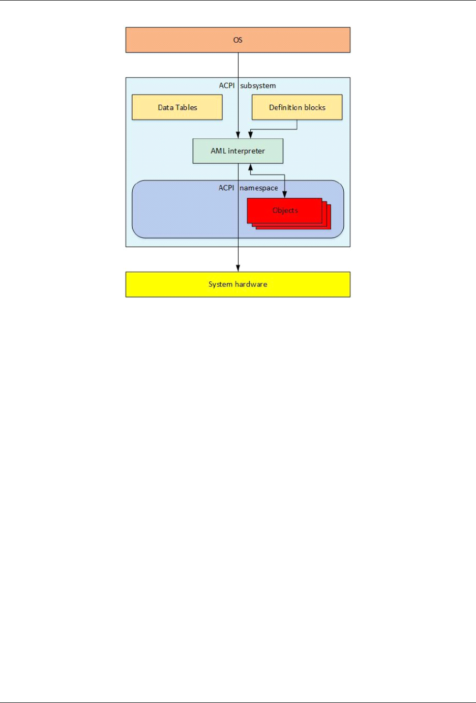
Advanced Configuration and Power Interface (ACPI) Specification, Release 6.5
Fig. 2: Fig. i-2 - ACPI Structure
can either have a directly defined value, or be evaluated by the AML interpreter. The AML interpreter, directed by the
OS, evaluates objects and then interfaces with system hardware to perform necessary operations.
The definition block byte code is compiled from the ACPI Source Language (ASL) code. ASL is the language used
to define ACPI objects and to write control methods. An ASL compiler translates ASL into ACPI Machine Language
(AML) byte code. AML is the language processed by the AML interpreter, as shown in figure i-3.
ACPI Source Language (ASL) code is used to define objects and control methods. Then the ASL compiler translates
ASL into ACPI Machine Language (AML) byte code contained within ACPI definition Blocks. Definition blocks
consist of an identifying table header and byte code that is executable by an AML interpreter.
The AML interpreter executes byte code and evaluates objects in the definition blocks to allow the byte code to perform
loop constructs, conditional evaluations, access defined address spaces, and perform other operations that applications
require. The AML interpreter has read/write access to defined address spaces, including system memory, I/O, PCI
configuration, and more. It accesses these address spaces by defining entry points called objects. Objects can either
have a directly defined value or else must be evaluated and interpreted by the AML interpreter.
This collection of enumerable objects is an OS construct called the ACPI namespace. The namespace is a hierarchical
representation of the ACPI devices on a system. The system bus is the root of enumeration for these ACPI devices.
Devices that are enumerable on other buses, like PCI or USB devices, are usually not enumerated in the namespace.
Instead, their own buses enumerate the devices and load their drivers. However, all enumerable buses have an encoding
technique that allows ACPI to encode the bus-specific addresses of the devices so they can be found in ACPI, even
though ACPI usually does not load drivers for these devices.
Generally, devices that have a _HID object (hardware identification object) are enumerated and have their drivers
loaded by ACPI. Devices that have an _ADR object (physical address object) are usually not enumerated by ACPI and
generally do not have their drivers loaded by ACPI. _ADR devices usually can perform all necessary functions without
involving ACPI, but in cases where the device driver cannot perform a function, or if the driver needs to communicate
to system firmware, ACPI can evaluate objects to perform the needed function.
As an example of this, PCI does not support native hotplug. However, PCI can use ACPI to evaluate objects and define
CONTENTS lxii

Advanced Configuration and Power Interface (ACPI) Specification, Release 6.5
Fig. 3: Fig. i-3 - ASL and AML
CONTENTS lxiii

Advanced Configuration and Power Interface (ACPI) Specification, Release 6.5
methods that allow ACPI to fill in the functions necessary to perform hotplug on PCI.
An additional aspect of ACPI is a runtime model that handles any ACPI interrupt events that occur during system
operation. ACPI continues to evaluate objects as necessary to handle these events. This interrupt-based runtime model
is discussed in greater detail in the Runtime model section below.
ACPI Initialization
The best way to understand how ACPI works is chronologically. The moment the user powers up the system, the
system firmware completes its setup, initialization, and self tests.
The system firmware then uses information obtained during firmware initialization to update the ACPI tables as nec-
essary with various platform configurations and power interface data, before passing control to the bootstrap loader.
The extended root system description table (XSDT) is the first table used by the ACPI subsystem and contains the ad-
dresses of most of the other ACPI tables on the system. The XSDT points to the fixed ACPI description table (FADT)
as well as other major tables that the OS processes during initialization. After the OS initializes, the FADT directs
the ACPI subsystem to the differentiated system description table (DSDT), which is the beginning of the namespace
because it is the first table that contains a definition block.
The ACPI subsystem then processes the DSDT and begins building the namespace from the ACPI definition blocks.
The XSDT also points to the secondary system description tables (SSDTs) and adds them to the namespace. The ACPI
data tables give the OS raw data about the system hardware.
After the OS has built the namespace from the ACPI tables, it begins traversing the namespace and loading device
drivers for all the _HID devices it encounters in the namespace. See figure i-4.
In the ACPI Intialization diagram above, system firmware updates the ACPI tables as necessary with information only
available at runtime, before handing off control to the bootstrap loader. The XSDT is the first table used by the OS’s
ACPI subsystem, and contains addresses of most other ACPI tables on the system. The XSDT points to the FADT, the
SSDTs, and other major ACPI tables. The FADT directs the ACPI subsystem to the DSDT, which is the beginning of
the namespace because DSDT is the first table that contains a definition block. The ACPI subsystem then consumes
the DSDT and begins building the ACPI namespace from the definition blocks. The XSDT also points to the SSDTs
and adds them to the namespace.
Runtime Model
After the system is up and running, ACPI works with the OS to handle any ACPI events that occur via an interrupt.
This interrupt invokes ACPI events in one of two general ways: fixed events and general purpose events (GPEs).
Fixed events are ACPI events that have a predefined meaning in the ACPI specification. These fixed events include
actions like pressing the power button or ACPI timer overflows. These events are handled directly by the OS handlers.
GPEs are ACPI events that are not predefined by the ACPI specification. These events are usually handled by evaluat-
ing control methods, which are objects in the namespace and can access system hardware. When the ACPI subsystem
evaluates the control method with the AML interpreter, the GPE object handles the events according to the OS’s im-
plementation. Typically this might involve issuing a notification to a device to invoke the device driver to perform a
function.
We discuss a generic example of this runtime model in the next section.
Thermal Event Example
ACPI includes a thermal model to allow systems to control the system temperature either actively (by performing
actions like turning a fan on) or passively by reducing the amount of power the system uses (by performing actions
like throttling the processor). We can use an example of a generic thermal event shown in Figure i-5 to demonstrate
how the ACPI runtime model works.
The ACPI thermal zone includes control methods to read the current system temperature and trip points.
When the OS initially finds a thermal zone in the namespace, it loads the thermal zone driver, which evaluates the
thermal zone to obtain the current temperature and trip points.
CONTENTS lxiv

Advanced Configuration and Power Interface (ACPI) Specification, Release 6.5
Fig. 4: Fig. i-4 ACPI Initialization
CONTENTS lxv

Advanced Configuration and Power Interface (ACPI) Specification, Release 6.5
Fig. 5: Fig. i-5 Runtime Thermal Event
CONTENTS lxvi

Advanced Configuration and Power Interface (ACPI) Specification, Release 6.5
When a system component heats up enough to trigger a trip point, a thermal zone GPE occurs.
The GPE causes an interrupt to occur. When the ACPI subsystem receives the interrupt, it first checks whether any
fixed events have occurred. In this example, the thermal zone event is a GPE, so no fixed event has occurred.
The ACPI subsystem then searches the namespace for the control method that matches the GPE number of the inter-
rupt. Upon finding it, the ACPI subsystem evaluates the control method, which might then access hardware and/or
notify the thermal zone handler.
The operating system’s thermal zone handler then takes whatever actions are necessary to handle the event, including
possibly accessing hardware.
ACPI is a very robust interface implementation. The thermal zone trip point could notify the system to turn on a fan,
reduce a device’s performance, read the temperature, shut down the system, or any combination of these and other
actions depending on the need.
This runtime model is used throughout the system to manage all of the ACPI events that occur during system operation.
Summary
ACPI can best be described as a framework of concepts and interfaces that are implemented to form a subsystem
within the host OS. The ACPI tables, handlers, interpreter, namespace, events, and interrupt model together form this
implementation of ACPI, creating the ACPI subsystem within the host OS. In this sense, ACPI is the interface between
the system hardware/firmware and the OS and OS applications for configuration and power management. This gives
various OS a standardized way to support power management and configuration via the ACPI namespace.
The ACPI namespace is the enumerable, hierarchical representation of all ACPI devices on the system and is used to
both find and load drivers for ACPI devices on the system. The namespace can be dynamic by evaluating objects and
sending interrupts in real time, all without the need for the OS to call native system firmware code. This enables device
manufacturers to code their own instructions and events into devices. It also reduces incompatibility and instability by
implementing a standardized power management interface.
CONTENTS lxvii

CHAPTER
ONE
INTRODUCTION
The Advanced Configuration and Power Interface (ACPI) specification was developed to establish industry common
interfaces enabling robust operating system (OS)-directed motherboard device configuration and power management
of both devices and entire systems. ACPI is the key element in Operating System-directed configuration and Power
Management (OSPM).
ACPI evolved the existing pre-ACPI collection of power management BIOS code, Advanced Power Management
(APM) application programming interfaces (APIs, PNPBIOS APIs, Multiprocessor Specification (MPS) tables and
so on into a well-defined power management and configuration interface specification. ACPI provides the means
for an orderly transition from existing (legacy) hardware to ACPI hardware, and it allows for both ACPI and legacy
mechanisms to exist in a single machine and to be used as needed.
Further, system architectures being built at the time of the original ACPI specification’s inception, stretched the lim-
its of historical “Plug and Play” interfaces. ACPI evolved existing motherboard configuration interfaces to support
advanced architectures in a more robust, and potentially more efficient manner.
The interfaces and OSPM concepts defined within this specification are suitable to all classes of computers including
(but not limited to) desktop, mobile, workstation, and server machines. From a power management perspective,
OSPM/ACPI promotes the concept that systems should conserve energy by transitioning unused devices into lower
power states including placing the entire system in a low-power state (sleeping state) when possible.
This document describes ACPI hardware interfaces, ACPI software interfaces and ACPI data structures that, when
implemented, enable support for robust OS-directed configuration and power management (OSPM).
1.1 Principal Goals
ACPI is the key element in implementing OSPM. ACPI-defined interfaces are intended for wide adoption to encourage
hardware and software vendors to build ACPI-compatible (and, thus, OSPM-compatible) implementations.
The principal goals of ACPI and OSPM are to:
• Enable all computer systems to implement motherboard configuration and power management functions, using
appropriate cost/function tradeoffs:
– Computer systems include (but are not limited to) desktop, mobile, workstation, and server machines.
– Machine implementers have the freedom to implement a wide range of solutions, from the very simple to
the very aggressive, while still maintaining full OS support.
– Wide implementation of power management will make it practical and compelling for applications to
support and exploit it. It will make new uses of PCs practical and existing uses of PCs more economical.
• Enhance power management functionality and robustness:
1

Advanced Configuration and Power Interface (ACPI) Specification, Release 6.5
– Power management policies too complicated to implement in platform firmware can be implemented and
supported in the OS, allowing inexpensive power managed hardware to support very elaborate power
management policies.
– Gathering power management information from users, applications, and the hardware together into the OS
will enable better power management decisions and execution.
– Unification of power management algorithms in the OS will reduce conflicts between the firmware and OS
and will enhance reliability.
• Facilitate and accelerate industry-wide implementation of power management:
– OSPM and ACPI reduces the amount of redundant investment in power management throughout the in-
dustry, as this investment and function will be gathered into the OS. This will allow industry participants
to focus their efforts and investments on innovation rather than simple parity.
– The OS can evolve independently of the hardware, allowing all ACPI-compatible machines to gain the
benefits of OS improvements and innovations.
• Create a robust interface for configuring motherboard devices:
– Enable new advanced designs not possible with existing interfaces.
1.1.1 Principle of Inclusive Terminology
The UEFI Forum follows a Principle of Inclusive Terminology in building and maintaining content for specifications.
This means efforts are made to ensure that all wording is perceived or likely to be perceived as welcoming by everyone
regardless of personal characteristics. In some cases, the Forum acknowledges that wording derived from earlier
work, for example references to legacy specifications not controlled by the Forum, may not follow this principle. In
order to preserve compatibility for code that reads on legacy specifications, particularly where that specification is no
longer under maintenance or development, language in this specification may appear out of sync with this principle.
The Forum is resolved to work with other standards development bodies to eliminate such examples over time. In
the meanwhile, by acknowledging and calling attention to this issue the hope is to promote discussion and action
towards more complete use of Inclusive Language reflective of the diverse and innovative population of the technical
community that works on standards.
1.2 Power Management Rationale
It is necessary to move power management into the OS and to use an abstract interface (ACPI) between the OS and
the hardware to achieve the principal goals set forth above. Because ACPI is abstract, the OS can evolve separately
from the hardware and, likewise, the hardware from the OS.
ACPI is by nature more portable across operating systems and processors. ACPI control methods allow for very
flexible implementations of particular features.
Issues with older power management approaches include the following:
• Minimal support for power management inhibits application vendors from supporting or exploiting it.
– Moving power management functionality into the OS makes it available on every machine on which the
OS is installed. The level of functionality (power savings, and so on) varies from machine to machine, but
users and applications will see the same power interfaces and semantics on all OSPM machines.
– This will enable application vendors to invest in adding power management functionality to their products.
• Legacy power management algorithms were restricted by the information available to the platform firmware that
implemented them. This limited the functionality that could be implemented.
1.2. Power Management Rationale 2

Advanced Configuration and Power Interface (ACPI) Specification, Release 6.5
– Centralizing power management information and directives from the user, applications, and hardware in
the OS allows the implementation of more powerful functionality. For example, an OS can have a policy
of dividing I/O operations into normal and lazy. Lazy I/O operations (such as a word processor saving
files in the background) would be gathered up into clumps and done only when the required I/O device is
powered up for some other reason. A non-lazy I/O request made when the required device was powered
down would cause the device to be powered up immediately, the non-lazy I/O request to be carried out,
and any pending lazy I/O operations to be done. Such a policy requires knowing when I/O devices are
powered up, knowing which application I/O requests are lazy, and being able to assure that such lazy I/O
operations do not starve.
• Appliance functions, such as answering machines, require globally coherent power decisions. For example, a
telephone-answering application could call the OS and assert, “I am waiting for incoming phone calls; any sleep
state the system enters must allow me to wake and answer the telephone in 1 second.” Then, when the user
presses the “off” button, the system would pick the deepest sleep state consistent with the needs of the phone
answering service.
– Platform firmware has become very complex to deal with power management. It is difficult to make work
with an OS and is limited to static configurations of the hardware.
– There is much less state information for the platform firmware to retain and manage (because the OS
manages it).
– Power management algorithms are unified in the OS, yielding much better integration between the OS and
the hardware.
– Because additional ACPI tables (Definition Blocks) can be loaded, for example, when a mobile system
docks, the OS can deal with dynamic machine configurations.
– Because the platform firmware has fewer functions and they are simpler, it is much easier (and therefore
cheaper) to implement and support.
1.3 Legacy Support
ACPI provides support for an orderly transition from legacy hardware to ACPI hardware, and allows for both mecha-
nisms to exist in a single machine and be used as needed.
Table 1.1: Hardware Type vs. OS Type Interaction
Hardware/OS Legacy OS ACPI OS with OSPM
Legacy hardware A legacy OS on legacy
hardware does what it al-
ways did.
If the OS lacks legacy support, legacy support is com-
pletely contained within the hardware functions.
Legacy and ACPI hard-
ware support in machine
It works just like a legacy
OS on legacy hardware.
During boot, the OS tells the hardware to switch from
legacy to OSPM/ACPI mode and from then on, the sys-
tem has full OSPM/ACPI support.
ACPI-only hardware There is no power man-
agement.
There is full OSPM/ACPI support.
1.3. Legacy Support 3

Advanced Configuration and Power Interface (ACPI) Specification, Release 6.5
1.4 OEM Implementation Strategy
Any OEM is, as always, free to build hardware as they see fit. Given the existence of the ACPI specification, two
general implementation strategies are possible:
• An original equipment manufacturer (OEM) can adopt the OS vendor-provided ACPI OSPM software and
implement the hardware part of the ACPI specification (for a given platform) in one of many possible ways.
• An OEM can develop a driver and hardware that are not ACPI-compatible. This strategy opens up even more
hardware implementation possibilities. However, OEMs who implement hardware that is OSPM-compatible but
not ACPI-compatible will bear the cost of developing, testing, and distributing drivers for their implementation.
1.5 Power and Sleep Buttons
OSPM provides a new appliance interface to consumers. In particular, it provides for a sleep button that is a “soft”
button that does not turn the machine physically off but signals the OS to put the machine in a soft off or sleeping state.
ACPI defines two types of these “soft” buttons: one for putting the machine to sleep and one for putting the machine
in soft off.
This gives the OEM two different ways to implement machines: A one-button model or a two-button model. The one-
button model has a single button that can be used as a power button or a sleep button as determined by user settings.
The two-button model has an easily accessible sleep button and a separate power button. In either model, an override
feature that forces the machine to the soft-off state without OSPM interaction is also needed to deal with various rare,
but problematic, situations.
1.6 ACPI Specification and the Structure of ACPI
This specification defines ACPI hardware interfaces, ACPI software interfaces and ACPI data structures. This specifi-
cation also defines the semantics of these interfaces.
Fig. 1.1 below lays out the software and hardware components for OSPM/ACPI, and how they relate to each other.
This specification describes the interfaces between components, the contents of the ACPI System Description Tables,
and the related semantics of the other ACPI components. Notice that the ACPI System Description Tables, which
describe a particular platform’s hardware, are at heart of the ACPI implementation and the role of the ACPI System
Firmware is primarily to supply the ACPI Tables (rather than a native instruction API).
ACPI is not a software specification; it is not a hardware specification, although it addresses both software and hard-
ware and how they must behave. ACPI is, instead, an interface specification comprised of both software and hardware
elements.
There are three run-time components to ACPI:
ACPI System Description Tables
Describes the interfaces to the hardware. Some descriptions limit what can be built (for example, some controls are
embedded in fixed blocks of registers and the table specifies the address of the register block). Most descriptions
allow the hardware to be built in arbitrary ways and can describe arbitrary operation sequences needed to make the
hardware function. ACPI Tables containing “Definition Blocks” can make use of a pseudo-code type of language,
the interpretation of which is performed by the OS. That is, OSPM contains and uses an interpreter that executes
procedures encoded in the pseudo-code language and stored in the ACPI tables containing “Definition Blocks.” The
pseudo-code language, known as ACPI Machine Language (AML), is a compact, tokenized, abstract type of machine
language.
ACPI Registers
1.4. OEM Implementation Strategy 4

Advanced Configuration and Power Interface (ACPI) Specification, Release 6.5
Fig. 1.1: OSPM/ACPI Global System
1.6. ACPI Specification and the Structure of ACPI 5

Advanced Configuration and Power Interface (ACPI) Specification, Release 6.5
The constrained part of the hardware interface, described (at least in location) by the ACPI System Description Tables.
ACPI Platform Firmware
Refers to the portion of the firmware that is compatible with the ACPI specifications. Typically, this is the code that
boots the machine (as legacy BIOSs have done) and implements interfaces for sleep, wake, and some restart operations.
It is called rarely, compared to a legacy BIOS. The ACPI Description Tables are also provided by the ACPI Platform
Firmware.
1.7 OS and Platform Compliance
The ACPI specification contains only interface specifications. ACPI does not contain any platform compliance re-
quirements. The following sections provide guidelines for class specific platform implementations that reference
ACPI-defined interfaces and guidelines for enhancements that operating systems may require to completely support
OSPM/ACPI. The minimum feature implementation requirements of an ACPI-compatible OS are also provided.
1.7.1 Platform Implementations of ACPI-defined Interfaces
System platforms implement ACPI-defined hardware interfaces via the platform hardware and ACPI-defined software
interfaces and system description tables via the ACPI system firmware. Specific ACPI-defined interfaces and OSPM
concepts while appropriate for one class of machine (for example, a mobile system), may not be appropriate for
another class of machine (for example, a multi-domain enterprise server). It is beyond the capability and scope of this
specification to specify all platform classes and the appropriate ACPI-defined interfaces that should be required for the
platform class.
Platform design guide authors are encouraged to require the appropriate ACPI-defined interfaces and hardware require-
ments suitable to the particular system platform class addressed in a particular design guide. Platform design guides
should not define alternative interfaces that provide similar functionality to those defined in the ACPI specification.
1.7.1.1 Recommended Features and Interface Descriptions for Design Guides
Common description text and category names should be used in design guides to describe all features, concepts, and
interfaces defined by the ACPI specification as requirements for a platform class. Listed below is the recommended
set of high-level text and category names to be used to describe the features, concepts, and interfaces defined by ACPI.
Note: The definitions and relational requirements of the interfaces specified below are generally spread throughout
the ACPI specification:
• System Address Map Interfaces
• ACPI System Description Tables
• Root System Description Pointer (RSDP)
• System Description Table Header
• Root System Description Table (RSDT)
• Fixed ACPI Description Table (FADT)
• Firmware ACPI Control Structure (FACS)
• Differentiated System Description Table (DSDT)
• Secondary System Description Table (SSDT)
1.7. OS and Platform Compliance 6

Advanced Configuration and Power Interface (ACPI) Specification, Release 6.5
• Multiple APIC Description Table (MADT)
• Smart Battery Table (SBST)
• Extended System Description Table (XSDT)
• Embedded Controller Boot Resources Table (ECDT)
• System Resource Affinity Table (SRAT)
• System Locality information Table
• Corrected Platform Error Polling Table (CPEP)
• Maximum System Characteristics Table (MSCT)
• ACPI RAS Feature Table (RASF)
• ACPI RAS2 Feature Table (RAS2)
• Memory Power State Table (MPST)
• Platform Memory Topology Table
• Boot Graphics Resource Table (BGRT)
• Firmware Performance Data Table (FPDT)
• Generic Timer Description Table (GTDT)
• Fixed ACPI Description Table (FADT)
• Power management timer control/status
• Power or sleep button with S5 override (also possible in generic space)
• Real time clock wakeup alarm control/status
• SCI /SMI routing control/status for Power Management and General-purpose events
• System power state controls (sleeping/wake control)
• Processor power state control (c states)
• Processor throttling control/status
• Processor performance state control/status
• General-purpose event control/status
• Global Lock control/status
• System Reset control
• Embedded Controller control/status
• SMBus Host Controller (HC) control/status
• Smart Battery Subsystem
• ACPI-defined Generic Register Interfaces and object definitions in the ACPI Namespace.
• General-purpose event processing
• Motherboard device identification, configuration, and insertion/removal
• Thermal zones
• Power resource control
• Device power state control
1.7. OS and Platform Compliance 7

Advanced Configuration and Power Interface (ACPI) Specification, Release 6.5
• System power state control
• System indicators
• Devices and device controls:
– Processor
– Control Method Battery
– Smart Battery Subsystem
– Mobile Lid
– Power or sleep button with S5 override (also possible in fixed space)
– Embedded controller
– Fan
– Generic Bus Bridge
– ATA Controller
– Floppy Controller
– GPE Block
– Module
– Memory
• Global Lock related interfaces
• ACPI Event programming model
• ACPI-defined Platform Firmware Responsibilities
• ACPI-defined State Definitions:
– Global system power states (G-states, S0, S5)
– System sleeping states (S-states S1-S4)
– Device power states (D-states)
– Processor power states (C-states)
– Device and processor performance states (P-states)
1.7.1.2 Terminology Examples for Design Guides
The following example shows how a client platform design guide could use the recommended terminology to define
ACPI requirements, with a goal of requiring robust configuration and power management for the system class.
Note: This example is provided as a guideline for how ACPI terminology can be used. It should not be interpreted as
a statement of ACPI requirements.
Platforms compliant with this platform design guide must implement the following ACPI defined system features,
concepts, and interfaces, along with their associated event models:
• System Address Map Interfaces
• ACPI System Description Tables provided in the system firmware
• ACPI-defined Fixed Registers Interfaces:
1.7. OS and Platform Compliance 8

Advanced Configuration and Power Interface (ACPI) Specification, Release 6.5
• Power management timer control/status
• Power or sleep button with S5 override (may also be implemented in generic register space)
• Real time clock wakeup alarm control/status
• General-purpose event control/status
• SCI /SMI routing control/status for Power Management and General-purpose events (control required only if
system supports legacy mode)
• System power state controls (sleeping/wake control)
• Processor power state control (for C1)
• Global Lock control/status (if Global Lock interfaces are required by the system)
• ACPI-defined Generic Register Interfaces and object definitions in the ACPI Namespace:
– General-purpose event processing
– Motherboard device identification, configuration, and insertion/removal
– System power state control ( Section 7.3)
– Devices and device controls:
*
Processor
*
Control Method Battery (or Smart Battery Subsystem on a mobile system)
*
Smart Battery Subsystem (or Control Method Battery on a mobile system)
*
Power or sleep button with S5 override (may also be implemented in fixed register space)
– Global Lock related interfaces when a logical register in the hardware is shared between OS and firmware
environments
• ACPI Event programming model
• ACPI-defined Platform Firmware Responsibilities
• ACPI-defined State Definitions:
– System sleeping states (At least one system sleeping state, S1-S4, must be implemented)
– Device power states (D-states must be implemented in accordance with device class specifications)
– Processor power states (All processors must support the C1 Power State)
The following example shows how a design guide could use the recommended terminology to define ACPI related
requirements for systems that execute multiple OS instances, with a goal of requiring robust configuration and contin-
uous availability for the system class.
Note: This example is provided as a guideline for how ACPI terminology can be used. It should not be interpreted as
a statement of ACPI requirements.
Platforms compliant with this platform design guide must implement the following ACPI defined system features and
interfaces, along with their associated event models:
• System Address Map Interfaces
• ACPI System Description Tables provided in the system firmware
• ACPI-defined Fixed Registers Interfaces:
• Power management timer control/status
1.7. OS and Platform Compliance 9

Advanced Configuration and Power Interface (ACPI) Specification, Release 6.5
• General-purpose event control/status
• SCI /SMI routing control/status for Power Management and General-purpose events
• (control required only if system supports legacy mode)
• System power state controls (sleeping/wake control)
• Processor power state control (for C1)
• Global Lock control/status (if Global Lock interfaces are required by the system)
• ACPI-defined Generic Register Interfaces and object definitions in the ACPI Namespace:
– General-purpose event processing
– Motherboard device identification, configuration, and insertion/removal (Section 6)
– System power state control (Section 7.3)
– System indicators
– Devices and device controls:
*
Processor
• Global Lock related interfaces when a logical register in the hardware is shared between OS and firmware
environments
• ACPI Event programming model (Section 5.6)
• ACPI-defined Platform Firmware Responsibilities (Section 15)
• ACPI-defined State Definitions:
Processor power states (All processors must support the C1 Power State)
1.7.2 OSPM Implementations
OS enhancements are needed to support ACPI-defined features, concepts, and interfaces, along with their associated
event models appropriate to the system platform class upon which the OS executes. This is the implementation of
OSPM. The following outlines the OS enhancements and elements necessary to support all ACPI-defined interfaces.
To support ACPI through the implementation of OSPM, the OS needs to be modified to:
• Use System Address Map Interfaces.
• Find and consume the ACPI System Description Tables.
• Interpret ACPI machine language (AML).
• Enumerate and configure motherboard devices described in the ACPI Namespace.
• Interface with the power management timer.
• Interface with the real-time clock wake alarm.
• Enter ACPI mode (on legacy hardware systems).
• Implement device power management policy.
• Implement power resource management.
• Implement processor power states in the scheduler idle handlers.
• Control processor and device performance states.
• Implement the ACPI thermal model.
1.7. OS and Platform Compliance 10

Advanced Configuration and Power Interface (ACPI) Specification, Release 6.5
• Support the ACPI Event programming model including handling SCI interrupts, managing fixed events, general-
purpose events, embedded controller interrupts, and dynamic device support.
• Support acquisition and release of the Global Lock.
• Use the reset register to reset the system.
• Provide APIs to influence power management policy.
• Implement driver support for ACPI-defined devices.
• Implement APIs supporting the system indicators.
• Support all system states S1-S5.
1.7.3 OS Requirements
The following list describes the minimum requirements for an OSPM/ACPI-compatible OS:
• Use Section 15 to get the system address map on Intel Architecture (IA) platforms:
• INT 15H, E820H - Query System Address Map interface (see Section 15)
• EFI GetMemoryMap() Boot Services Function (see Section 15)
• Find and consume the ACPI System Description Tables (see Section 5).
• Implementation of an AML interpreter supporting all defined AML grammar elements (see Section 20).
• Support for the ACPI Event programming model including handling SCI interrupts, managing fixed events,
general-purpose events, embedded controller interrupts, and dynamic device support.
• Enumerate and configure motherboard devices described in the ACPI Namespace.
• Implement support for the following ACPI devices defined within this specification:
• Embedded Controller Device (see Section 12)
• GPE Block Device (see Section 9.9)
• Implementation of the ACPI thermal model (see Section 3.10).
• Support acquisition and release of the Global Lock.
• OS-directed power management support (device drivers are responsible for maintaining device context as de-
scribed by the Device Power Management Class Specifications described in Appendix A: Device Class Specifi-
cations).
1.8 Target Audience
This specification is intended for the following users:
• OEMs building hardware containing ACPI-compatible interfaces
• Operating system and device driver developers
• All platform system firmware developers
• CPU and chip set vendors
• Peripheral vendors
1.8. Target Audience 11

Advanced Configuration and Power Interface (ACPI) Specification, Release 6.5
1.9 Document Organization
The ACPI specification document is organized into the following four parts:
• The first part of the specification (chapters 1 through 3) introduces ACPI and provides an executive overview.
• The second part (chapters 4 and 5) defines the ACPI hardware and software programming models.
• The third part (chapters 6 through 17) specifies the ACPI implementation details; this part of the specification is
primarily for developers.
• The fourth part (chapters 18 and 19) is technical reference material: chapter 18 is the ACPI Source Language
(ASL) reference, which is referenced by many other sections in this specification.
• Appendices contain device class specifications, describing power management characteristics of specific classes
of devices, and device class-specific ACPI interfaces.
1.9.1 ACPI Introduction and Overview
The first three sections of the specification provide an executive overview of ACPI.
Chapter 1: Introduction Discusses the purpose and goals of the specification, presents an overview of the ACPI-
compatible system architecture, specifies the minimum requirements for an ACPI-compatible system, and pro-
vides references to related specifications.
Chapter 2: Definition of Terms Defines the key terminology used in this specification. In particular, the global sys-
tem states (Mechanical Off, Soft Off, Sleeping, Working, and Non-Volatile Sleep) are defined in this Chapter,
along with the device power state definitions: Off (D3), D3hot, D2, D1, and Fully-On (D0). Device and proces-
sor performance states (P0, P1, . . . Pn) are also discussed.
Chapter 3: ACPI Overview Gives an overview of the ACPI specification in terms of the functional areas covered by
the specification: system power management, device power management, processor power management, Plug
and Play, handling of system events, battery management, and thermal management.
1.9.2 Programming Models
Chapters 4 and 5 define the ACPI hardware and software programming models. This part of the specification is
primarily for system designers, developers, and project managers.
All of the implementation-oriented, reference, and platform example Chapters of the specification that follow (all the
rest of the Chapters of the specification) are based on the models defined in Chapters 4 and 5. These Chapters are the
heart of the ACPI specification. There are extensive cross-references between the two Chapters.
Chapter 4: ACPI Hardware Specification Defines a set of hardware interfaces that meet the goals of this specifica-
tion.
Chapter 5: ACPI Software Programming Model Defines a set of software interfaces that meet the goals of this
specification.
1.9. Document Organization 12

Advanced Configuration and Power Interface (ACPI) Specification, Release 6.5
1.9.3 Implementation Details
The third part of the specification defines the implementation details necessary to actually build components that work
on an ACPI-compatible platform. This part of the specification is primarily for developers.
Chapter 6: Configuration Defines the reserved Plug and Play objects used to configure and assign resources to
devices, and share resources and the reserved objects used to track device insertion and removal. Also defines
the format of ACPI-compatible resource descriptors.
Chapter 7: Power and Performance Management Defines the reserved device power-management objects and the
reserved-system power-management objects.
Chapter 8: Processor Configuration and Control Defines how the OS manages the processors’ power consumption
and other controls while the system is in the working state.
Chapter 9: ACPI-Specific Device Objects Lists the integrated devices that need support for some device-specific
ACPI controls, along with the device-specific ACPI controls that can be provided. Most device objects are
controlled through generic objects and control methods and have generic device IDs; this Chapter discusses the
exceptions.
Chapter 10: Power Source Devices Defines the reserved battery device and AC adapter objects.
Chapter 11: Thermal Management Defines the reserved thermal management objects.
Chapter 12: ACPI Embedded Controller Interface Specification Defines the interfaces between an ACPI-
compatible OS and an embedded controller.
Chapter 13: ACPI System Management Bus Interface Specification Defines the interfaces between an ACPI-
compatible OS and a System Management Bus (SMBus) host controller.
Chapter 14: Platform Communications Channel Explains the generic mechanism for OSPM to communicate with
an entity in the platform defines a new address space type.
Chapter 15: System Address Map Interfaces Explains the special INT 15 call for use in ISA/EISA/PCI bus-based
systems. This call supplies the OS with a clean memory map indicating address ranges that are reserved and
ranges that are available on the motherboard. UEFI-based memory address map reporting interfaces are also
described.
Chapter 16: Waking and Sleeping Defines in detail the transitions between system working and sleeping states and
their relationship to wake events. Refers to the reserved objects defined in Chapters 6, 7, and 8.
Chapter 17: Non-Uniform Memory Access (NUMA) Architecture Platforms Discusses in detail how ACPI de-
fine interfaces can be used to describe a NUMA architecture platform. Refers to the reserved objects defined in
Chapters 5, 6, 8, and 9.
Chapter 18: ACPI Platform Error Interfaces Defines interfaces that enable OSPM to processes different types of
hardware error events that are detected by platform-based error detection hardware.
1.9.4 Technical Reference
The fourth part of the specification contains reference material for developers.
Chapter 19: ACPI Source Language Reference Defines the syntax of all the ASL statements that can be used to
write ACPI control methods, along with example syntax usage.
Chapter 20: ACPI Machine Language Specification Defines the grammar of the language of the ACPI virtual ma-
chine language. An ASL translator (compiler) outputs AML.
Chapter 21: ACPI Data Tables and Table Language Definition Describes a simple language (the Table Definition
Language or TDL) that can be used to generate any ACPI data table.
1.9. Document Organization 13

Advanced Configuration and Power Interface (ACPI) Specification, Release 6.5
Appendix A: Device class specifications Describes device-specific power management behavior on a per device-
class basis.
Appendix B: Video Extensions Contains video device class-specific ACPI interfaces
1.9.5 Revsion Numbers
Updates to the ACPI specification are considered either new revisions or errata as described below:
• A new revision is produced when there is substantive new content or changes that may modify existing behavior.
New revisions are designated by a Major.Minor version number (e.g. 6.3). In cases where the changes are
exceptionally minor, we may have a Major.Minor.Minor naming convention (e.g. 6.3.1).
• An errata is produced when proposed changes or fixes of the specification do not include any significant new
material or modify existing behavior. Errata are designated by adding an upper-case letter at the end of the
version number, such as 6.2A.
1.10 Related Documents
Power management and Plug and Play specifications for legacy hardware platforms are available from Links to ACPI-
Related Documents:
• Advanced Power Management (APM) BIOS Specification
• Plug and Play BIOS Specification
Intel Architecture specifications are available at http://developer.intel.com and https://software.intel.com/en-us/
articles/intel-sdm.
Other UEFI Specifications are available at https://uefi.org/specifications:
• Unified Extensible Firmware Interface (UEFI) Specification
• Platform Integration (PI) Specification
Documentation and specifications for the Smart Battery System components and the SMBus are availabe at the fol-
lowing links:
• Smart Battery System specifications
• SMBus specifications
USB Power Delivery Specification (Revision 3.1, Version 1.3): see “Links to ACPI-Related Documents” (http://uefi.
org/acpi) under the heading “Universal Serial Bus Power Management”
1.10. Related Documents 14

CHAPTER
TWO
DEFINITION OF TERMS
This specification uses a particular set of terminology, defined in this section. This section has three parts:
General ACPI terms are defined and presented alphabetically.
The ACPI global system states (working, sleeping, soft off, and mechanical off) are defined. Global system states
apply to the entire system, and are visible to the user.
The ACPI device power states are defined. Device power states are states of particular devices; as such, they are
generally not visible to the user. For example, some devices may be in the off state even though the system as a whole
is in the working state. Device states apply to any device on any bus.
2.1 General ACPI Terminology
Advanced Configuration and Power Interface (ACPI) As defined in this document, ACPI is a method for describ-
ing hardware interfaces in terms abstract enough to allow flexible and innovative hardware implementations and
concrete enough to allow shrink-wrap OS code to use such hardware interfaces.
ACPI Hardware Computer hardware with the features necessary to support OSPM and with the interfaces to those
features described using the Description Tables as specified by this document.
ACPI Namespace A hierarchical tree structure in OS-controlled memory that contains named objects. These objects
may be data objects, control method objects, bus/device package objects, and so on. The OS dynamically
changes the contents of the namespace at run-time by loading definition blocks from the ACPI Tables that reside
in the ACPI system firmware. All the information in the ACPI Namespace comes from the Differentiated System
Description Table (DSDT), which contains the Differentiated Definition Block, and one or more other definition
blocks.
ACPI Machine Language (AML) Pseudo-code for a virtual machine supported by an ACPI-compatible OS and in
which ACPI control methods and objects are written. The AML encoding definition is provided in section 19,
“ACPI Machine Language (AML) Specification.”
Add-in Card A generic term used to refer to any device which can be inserted or removed from a platform through a
connection bus, such as PCI. Add-in cards are typically inserted within a platform’s physical enclosure, rather
than residing physically external to a platform. An add-in card will have its own devices and associated firmware,
and may have its own Expansion ROM Firmware.
Advanced Programmable Interrupt Controller (APIC) An interrupt controller architecture commonly found on
Intel Architecture-based 32-bit PC systems. The APIC architecture supports multiprocessor interrupt manage-
ment (with symmetric interrupt distribution across all processors), multiple I/O subsystem support, 8259A com-
patibility, and inter-processor interrupt support. The architecture consists of local APICs commonly attached
directly to processors and I/O APICs commonly in chip sets.
ACPI Source Language (ASL) The programming language equivalent for AML. ASL is compiled into AML im-
ages. The ASL statements are defined in section 18, “ACPI Source Language (ASL) Reference.”
15

Advanced Configuration and Power Interface (ACPI) Specification, Release 6.5
Address Range Scrub (ARS) Process by which regions of memory can be scrubbed to look for memory locations
that contain correctable or uncorrectable errors.
BIOS BIOS (Basic Input/Output System) is firmware that provides basic boot capabilities for a platform; it is used
here to refer specifically to traditional x86 BIOS, and not as a general term for all firmware, or a replacement
term for UEFI Core System BIOS. The ambiguity of this the term is what we are trying to remove. See also:
Legacy BIOS, System BIOS.
Boot Firmware Generic term to describe any firmware on a platform used during the boot process. Use a more
specific term, if possible.
Component Synonym for device. Please use the term “device” if possible.
Control Method A control method is a definition of how the OS can perform a simple hardware task. For example,
the OS invokes control methods to read the temperature of a thermal zone. Control methods are written in an
encoded language called AML that can be interpreted and executed by the ACPI-compatible OS. An ACPI-
compatible system must provide a minimal set of control methods in the ACPI tables. The OS provides a
set of well-defined control methods that ACPI table developers can reference in their control methods. OEMs
can support different revisions of chip sets with one version of platform firmware by either including control
methods in the platform firmware that test configurations and respond as needed or including a different set of
control methods for each chip set revision.
Central Processing Unit (CPU) or Processor The part of a platform that executes the instructions that do the work.
An ACPI-compatible OS can balance processor performance against power consumption and thermal states by
manipulating the processor performance controls. The ACPI specification defines a working state, labeled G0
(S0), in which the processor executes instructions. Processor sleeping states, labeled C1 through C3, are also
defined. In the sleeping states, the processor executes no instructions, thus reducing power consumption and,
potentially, operating temperatures. The ACPI specification also defines processor performance states, where
the processor (while in C0) executes instructions, but with lower performance and (potentially) lower power
consumption and operating temperature. For more information, see Section 8.
A definition block contains information about hardware implementation and configuration details in the form of
data and control methods, encoded in AML. An OEM can provide one or more definition blocks in the ACPI
Tables. One definition block must be provided: the Differentiated Definition Block, which describes the base
system. Upon loading the Differentiated Definition Block, the OS inserts the contents of the Differentiated
Definition Block into the ACPI Namespace. Other definition blocks, which the OS can dynamically insert and
remove from the active ACPI Namespace, can contain references to the Differentiated Definition Block. For
more information, see Definition Blocks.
Device A generic term used to refer to any computing, input/output or storage element, or any collection of computing,
input/output or storage elements, on a platform. An example of a device is a CPU, APU, embedded controller
(EC), BMC, Trusted Platform Module (TPM), graphics processing unit (GPU), network interface controller
(NIC), hard disk drive (HDD), solid state drive (SSD), Read Only Memory (ROM), flash ROM, or any of the
large number of other possible devices. If at all possible, use a more specific term.
Device Context The variable data held by the device; it is usually volatile. The device might forget this information
when entering or leaving certain states (for more information, see Device Power State Definitions), in which
case the OS software is responsible for saving and restoring the information. Device Context refers to small
amounts of information held in device peripherals. See System Context.
Device Firmware Firmware that is only used by a specific device and cannot be used with any other device. This
firmware is typically provided by the device manufacturer.
Differentiated System Description Table (DSDT) An OEM must supply a DSDT to an ACPI-compatible OS. The
DSDT contains the Differentiated Definition Block, which supplies the implementation and configuration in-
formation about the base system. The OS always inserts the DSDT information into the ACPI Namespace at
system boot time and never removes it.
Device Physical Address (DPA) A Device relative memory address.
2.1. General ACPI Terminology 16

Advanced Configuration and Power Interface (ACPI) Specification, Release 6.5
Embedded Controller The general class of micro-controllers used to support OEM-specific supports embedded con-
trollers in any platform design, as long as the micro-controller conforms to one of the models described in this
section. The embedded controller performs complex low-level functions through a simple interface to the host
microprocessor(s).
ACPI defines a standard hardware and software communications interface between an OS bus enumerator and
an embedded controller. This allows any OS to provide a standard bus enumerator that can directly communicate
with an embedded controller in the system, thus allowing other drivers within the system to communicate with
and use the resources of system embedded controllers. This in turn enables the OEM to provide platform features
that the OS and applications can use.
Embedded Controller Interface A standard hardware and software communications interface between an OS driver
and an embedded controller. This allows any OS to provide a standard driver that can directly communicate
with an embedded controller in the system, thus allowing other drivers within the system to communicate with
and use the resources of system embedded controllers (for example, Smart Battery and AML code). This in turn
enables the OEM to provide platform features that the OS and applications can use.
Expansion ROM Firmware Peripheral Component Interconnect (PCI) term for firmware executed on a host proces-
sor which is used by an add-in device during the boot process. This includes Option ROM Firmware and UEFI
drivers. Expansion ROM Firmware may be embedded as part of the Host Processor Boot Firmware, or may be
separate (e.g., from an add-in card). See also: Option ROM Firmware.
Firmware Generic term to describe any BIOS or firmware on a platform; it refers to the general class of things, not a
specific type. Use a more specific term, if possible.
Firmware ACPI Control Structure (FACS) A structure in read/write memory that the platform runtime firmware
uses for handshaking between the firmware and the OS. The FACS is passed to an ACPI-compatible OS via the
Fixed ACPI Description Table (FADT). The FACS contains the system’s hardware signature at last boot, the
firmware waking vector, and the Global Lock.
Firmware Storage Device A memory device used to store firmware. This could include Read Only Memory (ROM),
flash memory, eMMC, UFS drives, etc.
Fixed ACPI Description Table (FADT) A table that contains the ACPI Hardware Register Block implementation
and configuration details that the OS needs to directly manage the ACPI Hardware Register Blocks, as well
as the physical address of the DSDT, which contains other platform implementation and configuration details.
An OEM must provide an FADT to an ACPI-compatible OS in the RSDT/XSDT. The OS always inserts the
namespace information defined in the Differentiated Definition Block in the DSDT into the ACPI Namespace
at system boot time, and the OS never removes it.
Fixed Features A set of features offered by an ACPI interface. The ACPI specification places restrictions on where
and how the hardware programming model is generated. All fixed features, if used, are implemented as described
in this specification so that OSPM can directly access the fixed feature registers.
Fixed Feature Events A set of events that occur at the ACPI interface when a paired set of status and event bits in
the fixed feature registers are set at the same time. When a fixed feature event occurs, a system control interrupt
(SCI is raised. For ACPI fixed feature events, OSPM (or an ACPI-aware driver) acts as the event handler.
Fixed Feature Registers A set of hardware registers in fixed feature register space at specific address locations in
system I/O address space. ACPI defines register blocks for fixed features (each register block gets a separate
pointer from the FADT). For more information, see ACPI Hardware Features.
General-Purpose Event Registers The general-purpose event registers contain the event programming model for
generic features. All general-purpose events generate SCIs.
Generic Feature A generic feature of a platform is value-added hardware implemented through control methods and
general-purpose events.
Generic Interrupt Controller (GIC) An interrupt controller architecture for ARM processor-based systems.
2.1. General ACPI Terminology 17

Advanced Configuration and Power Interface (ACPI) Specification, Release 6.5
Global System Status Global system states apply to the entire system, and are visible to the user. The various global
system states are labeled G0 through G3 in the ACPI specification. For more information, see Global System
State Definitions.
Host Processor A host processor is the primary processing unit in a platform, traditionally called a Central Processing
Unit (CPU), now also sometimes referred to as an Application Processing Unit (APU), or a System on Chip
(SoC). This is the processing unit on which the primary operating system (and/or hypervisor), as well as user
applications run. This is the processor that is responsible for loading and executing the Host Processor Boot
Firmware. This term and “Boot Processor” should be considered synonyms for this particular text clean-up
effort (i.e., making them consistent should probably be part of a different ECR, if needed).
Host Processor Boot Firmware Generic term used to describe firmware loaded and executed by the Host Processor
which provides basic boot capabilities for a platform. This class of firmware is a reference to Legacy BIOS
and UEFI, which were sometimes referred to as System BIOS. Where the distinction between Legacy BIOS
and UEFI is not important, the term Host Processor Boot Firmware will be used. Where the distinction is
important, it will be referenced appropriately. Expansion ROM firmware may also be considered as part of the
Host Processor Boot Firmware. Expansion ROM Firmware may be embedded as part of the Host Processor
Boot Firmware, or may be separate from the Host Processor Boot Firmware (e.g., loaded from an add-in card).
Host Processor Runtime Firmware Host processor runtime firmware is any runtime firmware which executes on
the host processor.
Ignored Bits Some unused bits in ACPI hardware registers are designated as “ignored” in the ACPI specification.
Ignored bits are undefined and can return zero or one (in contrast to reserved bits, which always return zero).
Software ignores ignored bits in ACPI hardware registers on reads and preserves ignored bits on writes.
Intel Architecture-Personal Computer (IA-PC) A general descriptive term for computers built with processors
conforming to the architecture defined by the Intel processor family based on the Intel Architecture instruc-
tion set and having an industry-standard PC architecture.
I/O APIC An Input/Output Advanced Programmable Interrupt Controller routes interrupts from devices to the pro-
cessor’s local APIC.
I/O SAPIC An Input/Output Streamlined Advanced Programmable Interrupt Controller routes interrupts from de-
vices to the processor’s local APIC.
Label Storage Area A persistent storage area reserved for Label storage.
Legacy A computer state where power management policy decisions are made by the platform hardware/firmware
shipped with the system. The legacy power management features found in today’s systems are used to support
power management in a system that uses a legacy OS that does not support the OS-directed power management
architecture.
Legacy BIOS One form of Host Processor Boot Firmware used on x86 platforms which uses a legacy x86 BIOS
structure. This form of host processor boot firmware has been or is being replaced by UEFI. This term will
likely be most useful in distinguishing and comparing older forms of firmware to newer forms (e.g., “it was
done this way in legacy BIOS, but is now done another way in UEFI). See also: BIOS, System BIOS.
Legacy Hardware A computer system that has no ACPI or OSPM power management support.
Legacy OS An OS that is not aware of and does not direct the power management functions of the system. Included
in this category are operating systems with APM 1.x support.
Local APIC A local Advanced Programmable Interrupt Controller receives interrupts from the I/O APIC.
Local SAPIC A local Streamlined Advanced Programmable Interrupt Controller receives interrupts from the I/O
SAPIC.
Management Firmware Firmware used only by a Baseboard Management Controller (BMC) or other Out-of-Band
(OOB) management controller.
2.1. General ACPI Terminology 18

Advanced Configuration and Power Interface (ACPI) Specification, Release 6.5
Multiple APIC Description Table (MADT) The Multiple APIC Description Table (MADT) is used on systems
supporting the APIC and SAPIC to describe the APIC implementation. Following the MADT is a list of
APIC/SAPIC structures that declare the APIC/SAPIC features of the machine.
Namespace A namespace defines a contiguously-addressed range of Non-Volatile Memory, conceptually similar to
a SCSI Logical Unit (LUN) or an NVM Express namespace. A namespace can be described by one or more
Labels.
Non-Host Processor A non-host processor is a generic term used to describe any processing unit on a platform which
is not a host processor (e.g. a microcontroller, co-processor, etc). For the purposes of this particular ECR, this
should also be considered a synonym for “secondary processor”, those CPUs that might be on an SoC, for
example, that are not the host (or “boot”) processor.
NVDIMM Non Volatile Dual In-line Memory Module.
Object The nodes of the ACPI Namespace are objects inserted in the tree by the OS using the information in the
system definition tables. These objects can be data objects, package objects, control method objects, and so on.
Package objects refer to other objects. Objects also have type, size, and relative name.
Object name Part of the ACPI Namespace. There is a set of rules for naming objects.
Operating System-directed Power Management (OSPM) A model of power (and system) management in which
the OS plays a central role and uses global information to optimize system behavior for the task at hand.
Option ROM Firmware Legacy term for boot firmware typically executed on a host processor which is used by a
device during the boot process. Option ROM firmware may be included with the host processor boot firmware
or may be carried separately by a device (such as an add-in card). See also: Expansion ROM Firmware
Package An array of objects.
Peripheral A peripheral (also known as an external device) is a device which resides physically external to a platform
and is connected to a platform, either wired or wirelessly. A peripheral is comprised of its own devices which
may have their own firmware.
Persistent Memory (pmem) Byte-addressable memory that retains its contents across power loss.
Platform A platform consists of multiple devices assembled and working together to deliver a specific computing
function, but does not include any other software other than the firmware as part of the devices in the platform.
Examples of platforms include a notebook, a desktop, a server, a network switch, a blade, etc. - all without and
independent of any operating system, user applications, or user data.
Platform Boot Firmware The collection of all boot firmware on a platform. This firmware is initially loaded by a
platform (such as an SoC, a motherboard, or a complete system) at power-on to do basic initialization of the
platform hardware and then hand control to a boot loader or OS. In some cases this will be x86 BIOS, or it may
be UEFI Core System BIOS, or it could be something else entirely. Once control has been handed over to a boot
loader or an OS, this firmware has no further role.
Platform Runtime Firmware The collection of all run-time firmware on a platform. This is firmware that can pro-
vide functions that can be invoked by an OS, but those functions are still concerned only with the platform
hardware (e.g., PSCI on ARM). The assumption is that platform boot firmware has since been superceded by
the OS since the OS is now up and running, but that there is still a need for an OS to access specific features of
hardware that may only be possible via firmware.
Platform Firmware The collection of platform boot firmware and platform runtime firmware.
Power Button A user push button or other switch contact device that switches the system from the sleeping/soft off
state to the working state, and signals the OS to transition to a sleeping/soft off state from the working state.
Power Management Mechanisms in software and hardware to minimize system power consumption, manage system
thermal limits, and maximize system battery life. Power management involves trade-offs among system speed,
noise, battery life, processing speed, and alternating current (AC) power consumption. Power management
2.1. General ACPI Terminology 19

Advanced Configuration and Power Interface (ACPI) Specification, Release 6.5
is required for some system functions, such as appliance (for example, answering machine, furnace control)
operations.
Power Resources Resources (for example, power planes and clock sources) that a device requires to operate in a
given power state.
Power Sources The battery (including a UPS battery) and AC line powered adapters or power supplies that supply
power to a platform.
Register Grouping Consists of two register blocks (it has two pointers to two different blocks of registers). The
fixed-position bits within a register grouping can be split between the two register blocks. This allows the bits
within a register grouping to be split between two chips.
Reserved Bits Some unused bits in ACPI hardware registers are designated as “Reserved” in the ACPI specification.
For future extensibility, hardware-register reserved bits always return zero, and data writes to them have no side
effects. OSPM implementations must write zeros to all reserved bits in enable and status registers and preserve
bits in control registers.
Root System Description Pointer (RSDP) An ACPI-compatible system must provide an RSDP in the system’s low
address space. This structure’s only purpose is to provide the physical address of the RSDT and XSDT.
Root System Description Table (RSDT) A table with the signature ‘RSDT,’ followed by an array of physical point-
ers to other system description tables. The OS locates that RSDT by following the pointer in the RSDP structure.
Runtime Firmware Generic term to describe any firmware on a platform used during runtime (i.e., after the boot
process has completed). Use a more specific term, if possible.
Secondary System Description Table (SSDT) SSDTs are a continuation of the DSDT. Multiple SSDTs can be used
as part of a platform description. After the DSDT is loaded into the ACPI Namespace, each secondary descrip-
tion table listed in the RSDT/XSDT with a unique OEM Table ID is loaded. This allows the OEM to provide
the base support in one table, while adding smaller system options in other tables.
System Physical Address (SPA) The platform physical address assigned and programmed by the platform and uti-
lized by the OS.
Sleep Button A user push button that switches the system from the sleeping/soft off state to the working state, and
signals the OS to transition to a sleeping state from the working state.
Smart Battery Subsystem A battery subsystem that conforms to the following specifications: Smart Battery and
either Smart Battery System Manager or Smart Battery Charger and Selector–and the additional ACPI require-
ments.
Smart Battery Table An ACPI table used on platforms that have a Smart Battery subsystem. This table indicates
the energy-level trip points that the platform requires for placing the system into different sleeping states and
suggested energy levels for warning the user to transition the platform into a sleeping state.
SMBus Interface A standard hardware and software communications interface between an OS bus driver and an
SMBus controller.
Software Software is comprised of elements required to load the operating system and all user applications and user
data subsequently handled by the operating system.
Streamlined Advanced Programmable Interrupt Controller (SAPIC) An advanced APIC commonly found on
Intel Itanium
TM
Processor Family-based 64-bit systems.
System A system is the entirety of a computing entity, including all elements in a platform (hardware, firmware) and
software (operating system, user applications, user data). A system can be thought of both as a logical construct
(e.g. a software stack) or physical construct (e.g. a notebook, a desktop, a server, a network switch, etc).
System BIOS A term sometimes used in industry to refer to either Legacy BIOS, or to UEFI Core System BIOS, or
both. Please use this term only when referring to Legacy BIOS. See also: BIOS, Legacy BIOS.
System Context The volatile data in the system that is not saved by a device driver.
2.1. General ACPI Terminology 20

Advanced Configuration and Power Interface (ACPI) Specification, Release 6.5
System Control Interrupt (SCI) A system interrupt used by hardware to notify the OS of ACPI events. The SCI is
an active, low, shareable, level interrupt.
System Management Bus (SMBus) A two-wire interface based upon the I
2
C protocol. The SMBus is a low-speed
bus that provides positive addressing for devices, as well as bus arbitration.
System Management Interrupt (SMI) An OS-transparent interrupt generated by interrupt events on legacy systems.
By contrast, on ACPI systems, interrupt events generate an OS-visible interrupt that is shareable (edge-style
interrupts will not work). Hardware platforms that want to support both legacy operating systems and ACPI
systems must support a way of re-mapping the interrupt events between SMIs and SCIs when switching between
ACPI and legacy models.
Thermal States Thermal states represent different operating environment temperatures within thermal zones of a
system. A system can have one or more thermal zones; each thermal zone is the volume of space around a
particular temperature-sensing device. The transitions from one thermal state to another are marked by trip
points, which are implemented to generate an SCI when the temperature in a thermal zone moves above or
below the trip point temperature.
UEFI One form of Host Processor Boot Firmware which uses a Unified Extensible Firmware Interface (UEFI) struc-
ture (as defined by the UEFI Forum). This is the current host processor boot firmware structure being adopted
as a standard in the industry. This term should be used when referring specifically to UEFI code on a platform.
UEFI Drivers Standalone binary executables in PECOFF format which are loaded by UEFI during the boot process
to handle specific pieces of hardware.
eXtended Root System Description Table (XSDT) The XSDT provides identical functionality to the RSDT but ac-
commodates physical addresses of DESCRIPTION HEADERs that are larger than 32 bits. Notice that both the
XSDT and the RSDT can be pointed to by the RSDP structure.
2.2 Global System State Definitions
Global system states (Gx states) apply to the entire system and are visible to the user.
Global system states are defined by six principal criteria:
1. Does application software run?
2. What is the latency from external events to application response?
3. What is the power consumption?
4. Is an OS reboot required to return to a working state?
5. Is it safe to disassemble the computer?
6. Can the state be entered and exited electronically?
Following is a list of the system states:
G3 Mechanical Off A computer state that is entered and left by a mechanical means (for example, turning off the
system’s power through the movement of a large red switch). It is implied by the entry of this off state through a
mechanical means that no electrical current is running through the circuitry and that it can be worked on without
damaging the hardware or endangering service personnel. The OS must be restarted to return to the Working
state. No hardware context is retained. Except for the real-time clock, power consumption is zero.
G2/S5 Soft Off A computer state where the computer consumes a minimal amount of power. No user mode or system
mode code is run. This state requires a large latency in order to return to the Working state. The system’s context
will not be preserved by the hardware. The system must be restarted to return to the Working state. It is not safe
to disassemble the machine in this state.
2.2. Global System State Definitions 21

Advanced Configuration and Power Interface (ACPI) Specification, Release 6.5
G1 Sleeping A computer state where the computer consumes a small amount of power, user mode threads are not
being executed, and the system “appears” to be off (from an end user’s perspective, the display is off, and so
on). Latency for returning to the Working state varies on the wake environment selected prior to entry of this
state (for example, whether the system should answer phone calls). Work can be resumed without rebooting the
OS because large elements of system context are saved by the hardware and the rest by system software. It is
not safe to disassemble the machine in this state.
G0 Working A computer state where the system dispatches user mode (application) threads and they execute. In this
state, peripheral devices (peripherals) are having their power state changed dynamically. The user can select,
through some UI, various performance/power characteristics of the system to have the software optimize for
performance or battery life. The system responds to external events in real time. It is not safe to disassemble the
machine in this state.
S4 Non-Volatile Sleep A special global system state that allows system context to be saved and restored (relatively
slowly) when power is lost to the motherboard. If the system has been commanded to enter S4, the OS will
write all system context to a file on non-volatile storage media and leave appropriate context markers. The
machine will then enter the S4 state. When the system leaves the Soft Off or Mechanical Off state, transitioning
to Working (G0) and restarting the OS, a restore from a NVS file can occur. This will only happen if a valid
non-volatile sleep data set is found, certain aspects of the configuration of the machine have not changed, and
the user has not manually aborted the restore. If all these conditions are met, as part of the OS restarting, it will
reload the system context and activate it. The net effect for the user is what looks like a resume from a Sleeping
(G1) state (albeit slower). The aspects of the machine configuration that must not change include, but are not
limited to, disk layout and memory size. It might be possible for the user to swap a PC Card or a Device Bay
device, however.
Notice that for the machine to transition directly from the Soft Off or Sleeping states to S4, the system context must
be written to non-volatile storage by the hardware; entering the Working state first so that the OS or platform runtime
firmware can save the system context takes too long from the user’s point of view. The transition from Mechanical Off
to S4 is likely to be done when the user is not there to see it.
Because the S4 state relies only on non-volatile storage, a machine can save its system context for an arbitrary period
of time (on the order of many years).
Table 2.1: Summary of Global Power States
Global system
state
Software
runs
Latency Power con-
sumption
OS restart
required
Safe to dis-
assemble
computer
Exit state
electroni-
cally
G0 Working Yes 0 Large No No Yes
G1 Sleeping No >0, varies
with sleep
state
Smaller No No Yes
G2/S5 Soft Off No Long Very near 0 Yes No Yes
G3 Mechanical Off No Long RTC battery Yes Yes No
Notice that the entries for G2/S5 and G3 in the Latency column of the above table are “Long.” This implies that a
platform designed to give the user the appearance of “instant-on,” similar to a home appliance device, will use the G0
and G1 states almost exclusively (the G3 state may be used for moving the machine or repairing it).
2.2. Global System State Definitions 22

Advanced Configuration and Power Interface (ACPI) Specification, Release 6.5
2.3 Device Power State Definitions
Device power states are states of particular devices; as such, they are generally not visible to the user. For example,
some devices may be in the Off state even though the system as a whole is in the Working state.
Device states apply to any device on any bus. They are generally defined in terms of four principal criteria:
• Power consumption-How much power the device uses.
• Device context–How much of the context of the device is retained by the hardware. The OS is responsible for
restoring any lost device context (this may be done by resetting the device).
• Device driver–What the device driver must do to restore the device to full on.
• Restore time–How long it takes to restore the device to full on.
The device power states are defined below, although very generically. Many devices do not have all four power states
defined. Devices may be capable of several different low-power modes, but if there is no user-perceptible difference
between the modes, only the lowest power mode will be used. The Device Class Power Management Specifications,
included in Appendix A of this specification, describe which of these power states are defined for a given type (class)
of device and define the specific details of each power state for that device class. For a list of the available Device
Class Power Management Specifications, see Appendix A: Device Class Specifications.
D3 (Off) Power has been fully removed from the device. Also referred to as D3cold in this and other specs. All
device context is lost when this state is entered, so the OS software will reinitialize the device when powering it
back on. Since all device context and power are lost, devices in this state do not decode their address lines, and
cannot be enumerated by software. Devices in this state have the longest restore times.
D3hot The meaning of the D3hot State is defined by each device class. In general, D3hot is expected to save as
much power as possible without affecting PNP Enumeration. Devices in D3hot must have enough power to
remain enumerable by software. For example, PCI Configuration space access and contents must operate as in
shallower power states. Similarly, ACPI identification and configuration objects must operate as in shallower
power states. Otherwise, no device functionality is supported, and Driver software is required to restore any lost
context, or reinitialize the device, during its transition back to D0.
Devices in this state can have long restore times. All classes of devices define this state.
Note: For devices that support both D3hot and D3 exposed to OSPM via _PR3, device software/drivers must al-
ways assume OSPM will target D3and must assume all device context will be lost and the device will no longer be
enumerable.
D2 The meaning of the D2 Device State is defined by each device class. Many device classes may not define D2. In
general, D2 is expected to save more power and preserve less device context than D1 or D0. Buses in D2 may
cause the device to lose some context (for example, by reducing power on the bus, thus forcing the device to
turn off some of its functions).
D1 The meaning of the D1 Device State is defined by each device class. Many device classes may not define D1. In
general, D1 is expected to save less power and preserve more device context than D2.
D0 (Fully-On) This state is assumed to be the highest level of power consumption. The device is completely active
and responsive, and is expected to remember all relevant context continuously.
Transitions amongst these power states are restricted for simplicity. Power-down transitions (from higher-power, or
shallower, to lower-power, or deeper) are allowed between any two states. However, power-up transitions (from deeper
to shallower) are required to go through D0; i.e. Dy to Dx<y is illegal for all x !=0.
2.3. Device Power State Definitions 23

Advanced Configuration and Power Interface (ACPI) Specification, Release 6.5
Table 2.2: Summary of Device Power States
Device State Power Consumption Device Context Retained Driver Restoration
D0 - Fully-On As needed for operation All None
D1 D0>D1>D2> D3hot>D3 >D2 <D2
D2 D0>D1>D2> D3hot>D3 <D1 >D1
D3hot D0>D1>D2>D3hot>D3 Optional None <->Full initializa-
tion and load
D3 - Off 0 None Full initialization and load
Note: Devices often have different power modes within a given state. Devices can use these modes as long as they can
automatically transparently switch between these modes from the software, without violating the rules for the current
Dx state the device is in. Low-power modes that adversely affect performance (in other words, low speed modes) or
that are not transparent to software cannot be done automatically in hardware; the device driver must issue commands
to use these modes.
2.3.1 Device Performance States
Device performance states (Px states) are power consumption and capability states within the active (D0) device power
state. Performance states allow OSPM to make tradeoffs between performance and energy conservation. Device
performance states have the greatest impact when the implementation is such that the states invoke different device
efficiency levels as opposed to a linear scaling of performance and energy consumption. Since performance state
transitions occur in the active device states, care must be taken to ensure that performance state transitions do not
adversely impact the system.
Device performance states, when necessary, are defined on a per device class basis (See Appendix A: Device Class
Specifications for more information).
2.4 Sleeping and Soft-off State Definitions
S1-S4 are types of sleeping states within the global system state, G1, while S5 is a soft-off state associated with the
G2 system state. The Sx states are briefly defined below.
For a detailed definition of the system behavior within each Sx state, see \_Sx (System States). For a detailed definition
of the transitions between each of the Sx states, see Sleeping States.
S1 Sleeping State The S1 sleeping state is a low wake latency sleeping state. In this state, no system context is lost
(CPU or chip set) and hardware maintains all system context.
S2 Sleeping State The S2 sleeping state is a low wake latency sleeping state. This state is similar to the S1 sleeping
state except that the CPU and system cache context is lost (the OS is responsible for maintaining the caches and
CPU context). Control starts from the processor’s reset vector after the wake event.
S3 Sleeping State The S3 sleeping state is a low wake latency sleeping state where all system context is lost except
system memory. CPU, cache, and chip set context are lost in this state. Hardware maintains memory context
and restores some CPU and L2 configuration context. Control starts from the processor’s reset vector after the
wake event.
S4 Sleeping State The S4 sleeping state is the lowest power, longest wake latency sleeping state supported by ACPI.
In order to reduce power to a minimum, it is assumed that the hardware platform has powered off all devices.
Platform context is maintained.
2.4. Sleeping and Soft-off State Definitions 24

Advanced Configuration and Power Interface (ACPI) Specification, Release 6.5
S5 Soft Off State The S5 state is similar to the S4 state except that the OS does not save any context. The system
is in the “soft” off state and requires a complete boot when it wakes. Software uses a different state value to
distinguish between the S5 state and the S4 state to allow for initial boot operations within the platform boot
firmware to distinguish whether the boot is going to wake from a saved memory image.
2.5 Processor Power State Definitions
Processor power states (Cx states) are processor power consumption and thermal management states within the global
working state, G0. The Cx states possess specific entry and exit semantics and are briefly defined below. For a more
detailed definition of each Cx state, see Processor Power States.
C0 Processor Power State While the processor is in this state, it executes instructions.
C1 Processor Power State This processor power state has the lowest latency. The hardware latency in this state
must be low enough that the operating software does not consider the latency aspect of the state when deciding
whether to use it. Aside from putting the processor in a non-executing power state, this state has no other
software-visible effects.
C2 Processor Power State The C2 state offers improved power savings over the C1 state. The worst-case hardware
latency for this state is provided via the ACPI system firmware and the operating software can use this informa-
tion to determine when the C1 state should be used instead of the C2 state. Aside from putting the processor in
a non-executing power state, this state has no other software-visible effects.
C3 Processor Power State The C3 state offers improved power savings over the C1 and C2 states. The worst-case
hardware latency for this state is provided via the ACPI system firmware and the operating software can use this
information to determine when the C2 state should be used instead of the C3 state. While in the C3 state, the
processor’s caches maintain state but ignore any snoops. The operating software is responsible for ensuring that
the caches maintain coherency.
2.6 Device and Processor Performance State Definitions
Device and Processor performance states (Px states) are power consumption and capability states within the ac-
tive/executing states, C0 for processors and D0 for devices. The Px states are briefly defined below. For a more
detailed definition of each Px state from a processor perspective, see Processor Performance Control. For a more
detailed definition of each Px state from a device perspective see Device and Processor Performance States, and
Appendix A: Device Class Specifications.
P0 Performance State While a device or processor is in this state, it uses its maximum performance capability and
may consume maximum power.
P1 Performance State In this performance power state, the performance capability of a device or processor is limited
below its maximum and consumes less than maximum power.
Pn Performance State In this performance state, the performance capability of a device or processor is at its min-
imum level and consumes minimal power while remaining in an active state. State n is a maximum number
and is processor or device dependent. Processors and devices may define support for an arbitrary number of
performance states not to exceed 255.
2.5. Processor Power State Definitions 25

CHAPTER
THREE
ACPI CONCEPTS
Platforms compliant with the ACPI specification provide OSPM with direct and exclusive control over the power
management and motherboard device configuration functions of a computer. During OS initialization, OSPM takes
over these functions from legacy implementations such as the APM BIOS, SMM-based firmware, legacy applications,
and the PNPBIOS. Having done this, OSPM is responsible for handling motherboard device configuration events as
well as for controlling the power, performance, and thermal status of the system based on user preference, application
requests and OS imposed Quality of Service (QOS) / usability goals. ACPI provides low-level interfaces that allow
OSPM to perform these functions. The functional areas covered by the ACPI specification are:
System power management ACPI defines mechanisms for putting the computer as a whole in and out of system
sleeping states. It also provides a general mechanism for any device to wake the computer.
Device power management ACPI tables describe motherboard devices, their power states, the power planes the de-
vices are connected to, and controls for putting devices into different power states. This enables the OS to put
devices into low-power states based on application usage.
Processor power management While the OS is idle but not sleeping, it will use commands described by ACPI to
put processors in low-power states.
Device and processor performance management While the system is active, OSPM will transition devices and pro-
cessors into different performance states, defined by ACPI, to achieve a desirable balance between performance
and energy conservation goals as well as other environmental requirements (for example, visibility and acous-
tics).
Configuration / Plug and Play ACPI specifies information used to enumerate and configure motherboard devices.
This information is arranged hierarchically so when events such as docking and undocking take place, the OS
has precise, a priori knowledge of which devices are affected by the event.
System Events ACPI provides a general event mechanism that can be used for system events such as thermal events,
power management events, docking, device insertion and removal, and so on. This mechanism is very flexible
in that it does not define specifically how events are routed to the core logic chip set.
Battery management Battery management policy moves from the APM BIOS to the ACPI OS. An ACPI-compatible
battery device needs either a Smart Battery subsystem interface, which is controlled by the OS directly through
the embedded controller interface, or a Control Method Battery interface. A Control Method Battery interface
is completely defined by AML control methods, allowing an OEM to choose any type of the battery and any
kind of communication interface supported by ACPI. The battery must comply with the requirements of its
interface, as described either herein or in other applicable standards. The OS may choose to alter the behavior
of the battery, for example, by adjusting the Low Battery or Battery Warning trip point. When there are multiple
batteries present, the battery subsystem is not required to perform any synthesis of a “composite battery” from
the data of the separate batteries. In cases where the battery subsystem does not synthesize a “composite battery”
from the separate battery’s data, the OS must provide that synthesis.
Thermal management Since the OS controls the power and performance states of devices and processors, ACPI also
addresses system thermal management. It provides a simple, scalable model that allows OEMs to define thermal
zones, thermal indicators, and methods for cooling thermal zones.
26

Advanced Configuration and Power Interface (ACPI) Specification, Release 6.5
SMBus Controller ACPI defines a standard hardware and software communications interface between an OS bus
driver and an SMBus Controller. This allows any OS to provide a standard bus driver that can directly commu-
nicate with SMBus devices in the system. This in turn enables the OEM to provide platform features that the
OS and applications can use.
OSPM’s mission is to optimally configure the platform and to optimally manage the system’s power, performance,
and thermal status given the user’s preferences and while supporting OS imposed Quality of Service (QOS) / usability
goals. To achieve these goals, ACPI requires that once an ACPI compliant platform is in ACPI mode, the platform’s
hardware, firmware, or other non-OS software must not manipulate the platform’s configuration, power, performance,
and thermal control interfaces independently of OSPM. OSPM alone is responsible for coordinating the configuration,
power management, performance management, and thermal control policy of the system. Manipulation of these
interfaces independently of OSPM undermines the purpose of OSPM/ACPI and may adversely impact the system’s
configuration, power, performance, and thermal policy goals. There are two exceptions to this requirement. The first
is in the case of the possibility of damage to a system from an excessive thermal conditions where an ACPI compatible
OS is present and OSPM latency is insufficient to remedy an adverse thermal condition. In this case, the platform may
exercise a failsafe thermal control mechanism that reduces the performance of a system component to avoid damage.
If this occurs, the platform must notify OSPM of the performance reduction if the reduction is of significant duration
(in other words, if the duration of reduced performance could adversely impact OSPM’s power or performance control
policy - operating system vendors can provide guidance in this area). The second exception is the case where the
platform contains Active cooling devices but does not contain Passive cooling temperature trip points or controls,. In
this case, a hardware based Active cooling mechanism may be implemented without impacting OSPM’s goals. Any
platform that requires both active and passive cooling must allow OSPM to manage the platform thermals via ACPI
defined active and passive cooling interfaces.
3.1 System Power Management
Under OSPM, the OS directs all system and device power state transitions. Employing user preferences and knowledge
of how devices are being used by applications, the OS puts devices in and out of low-power states. Devices that are
not being used can be turned off. Similarly, the OS uses information from applications and user settings to put the
system as a whole into a low- power state. The OS uses ACPI to control power state transitions in hardware.
3.2 Power States
From a user-visible level, the system can be thought of as being in one of the states in the following diagram:
See Section 2.2 for detailed definitions of these states.
In general use, computers alternate between the Working and Sleeping states. In the Working state, the computer is
used to do work. User-mode application threads are dispatched and running. Individual devices can be in low-power
(Dx) states and processors can be in low-power (Cx) states if they are not being used. Any device the system turns off
because it is not actively in use can be turned on with short latency. (What “short” means depends on the device. An
LCD display needs to come on in sub-second times, while it is generally acceptable to wait a few seconds for a printer
to wake.)
The net effect of this is that the entire machine is functional in the Working state. Various Working sub-states differ
in speed of computation, power used, heat produced, and noise produced. Tuning within the Working state is largely
about trade-offs among speed, power, heat, and noise.
When the computer is idle or the user has pressed the power button, the OS will put the computer into one of the
sleeping (Sx) states. No user-visible computation occurs in a sleeping state. The sleeping sub-states differ in what
events can arouse the system to a Working state, and how long this takes. When the machine must awaken to all
possible events or do so very quickly, it can enter only the sub-states that achieve a partial reduction of system power
consumption. However, if the only event of interest is a user pushing on a switch and a latency of minutes is allowed,
3.1. System Power Management 27

Advanced Configuration and Power Interface (ACPI) Specification, Release 6.5
Fig. 3.1: Global System Power States and Transitions
the OS could save all system context into an NVS file and transition the hardware into the S4 sleeping state. In this
state, the machine draws almost zero power and retains system context for an arbitrary period of time (years or decades
if needed).
The other states are used less often. Computers that support legacy BIOS power management interfaces boot in the
Legacy state and transition to the Working state when an ACPI OS loads. A system without legacy support (for
example, a RISC system) transitions directly from the Mechanical Off state to the Working state. Users typically put
computers into the Mechanical Off state by flipping the computer’s mechanical switch or by unplugging the computer.
3.2.1 Power Button
In legacy systems, the power button typically either forces the machine into Soft Off or Mechanical Off or, on a laptop,
forces it to some sleeping state. No allowance is made for user policy (such as the user wants the machine to “come
on” in less than 1 second with all context as it was when the user turned the machine “off”), system alert functions
(such as the system being used as an answering machine or fax machine), or application function (such as saving a
user file).
In an OSPM system, there are two switches. One is to transition the system to the Mechanical Off state. A mechanism
to stop current flow is required for legal reasons in some jurisdictions (for example, in some European countries). The
other is the “main” power button. This is in some obvious place (for example, beside the keyboard on a laptop). Unlike
legacy on/off buttons, all it does is send a request to the system. What the system does with this request depends on
policy issues derived from user preferences, user function requests, and application data.
3.2. Power States 28

Advanced Configuration and Power Interface (ACPI) Specification, Release 6.5
3.2.2 Platform Power Management Characteristics
3.2.2.1 Mobile PC
Mobile PCs will continue to have aggressive power management functionality. Going to OSPM/ACPI will allow
enhanced power savings techniques and more refined user policies.
Aspects of mobile PC power management in the ACPI specification are thermal management (see Section 3.10).
3.2.2.2 Desktop PCs
Power-managed desktops will be of two types, though the first type will migrate to the second over time.
Ordinary “Green PC” Here, new appliance functions are not the issue. The machine is really only used for pro-
ductivity computations. At least initially, such machines can get by with very minimal function. In particular,
they need the normal ACPI timers and controls, but don’t need to support elaborate sleeping states, and so on.
They, however, do need to allow the OS to put as many of their devices/resources as possible into device standby
and device off states, as independently as possible (to allow for maximum compute speed with minimum power
wasted on unused devices). Such PCs will also need to support wake from the sleeping state by means of a
timer, because this allows administrators to force them to turn on just before people are to show up for work.
Home PC Computers are moving into home environments where they are used in entertainment centers and to per-
form tasks like answering the phone. A home PC needs all of the functionality of the ordinary green PC. In fact,
it has all of the ACPI power functionality of a laptop except for docking and lid events (and need not have any
legacy power management). Note that there is also a thermal management aspect to a home PC, as a home PC
user wants the system to run as quietly as possible, often in a thermally constrained environment.
3.2.2.3 Multiprocessor and Server PCs
Perhaps surprisingly, server machines often get the largest absolute power savings. Why? Because they have the
largest hardware configurations and because it’s not practical for somebody to hit the off switch when they leave at
night.
Day Mode In day mode, servers are power-managed much like a corporate ordinary green PC, staying in the Working
state all the time, but putting unused devices into low-power states whenever possible. Because servers can be
very large and have, for example, many disk spindles, power management can result in large savings. OSPM
allows careful tuning of when to do this, thus making it workable.
Night Mode In night mode, servers look like home PCs. They sleep as deeply as they can and are still able to wake
and answer service requests coming in over the network, phone links, and so on, within specified latencies. So,
for example, a print server might go into deep sleep until it receives a print job at 3 A.M., at which point it
wakes in perhaps less than 30 seconds, prints the job, and then goes back to sleep. If the print request comes
over the LAN, then this scenario depends on an intelligent LAN adapter that can wake the system in response
to an interesting received packet.
3.2. Power States 29

Advanced Configuration and Power Interface (ACPI) Specification, Release 6.5
3.3 Device Power Management
This section describes ACPI-compatible device power management. The ACPI device power states are introduced, the
controls and information an ACPI-compatible OS needs to perform device power management are discussed, the wake
operation devices use to wake the computer from a sleeping state is described, and an example of ACPI-compatible
device management using a modem is given
3.3.1 Device Power Management Model
ACPI Device Power Management is based on an integrated model consisting of:
Distributed device power state policy For each hardware device on the system, there is a Power Policy Owner in
the Operating System that is responsible for continuously determining the best power state for the device. The
best device power state is the one that, at any point in time, minimizes the consumption of power by the device
consistent with the usage requirements of the device by the system and its user. Policy is typically defined for
a class of devices, and incorporates application activity, user scenarios and other operating state as necessary. It
is applied to all devices of a given class.
Layered device power state control Once power state decisions are made for a device, they must be carried-out by
device drivers. The model partitions the control functionality between the device, bus and platform layers.
Device drivers at each layer perform control using mechanisms available at that level, coordinated by OSPM. In
general, the ordering proceeds from Device/Class level, to Bus level, to Platform level when a device is powering
down, and the inverse when powering-up.
For instance, a device-level driver has access, via the device programming interface, to settings and control
registers that invoke specific, sometimes proprietary, power control features in the device. The device driver
uses these controls as appropriate for the target ACPI-defined power state determined by the policy owner.
Similarly, classes of devices may have standardized power features, invoked in standardized ways that Class
Drivers might use when entering a target power state.
At the bus level, power management standards come into play to provide bus-specific controls that work for
every device connected to the bus, regardless of device class. PCI, for instance, defines fields in the device
Configuration Space for setting the device’s power state (D0-D3). Bus-level drivers utilize these standards to
perform control in addition to that applied by the device-specific or device class driver. Bus-specific mechanisms
also enable additional power savings in the system by enabling the bus infrastructure hardware itself to enter
lower power states, as defined in the bus standard.
Finally, for platform-level power state control, ACPI defines mechanisms (_PRx, _PSx, _ON, _OFF) for putting
a device into a given power state. The Operating System’s Power Management software (OSPM) utilizes these
mechanisms to execute the lowest-level, platform-specific control for a given device (such as turning power rails
and clocks off and on, resetting hardware, etc.).
Operating System coordination Finally, ACPI defines information and behavior requirements that enable OSPM to
inform the Power Policy Owner about supported state and wake-up capabilities, and to coordinate the actions
of the various levels of device drivers in controlling power. OSPM, in this role, is responsible for ensuring that
device power management is coordinated with System Power Management such as entering sleep states (S1-
S4) or Low-power Idle states (LPI). Integrated with device power state policy and control, wake-up policy and
control are also coordinated by OSPM. Power Policy Owners, which decide when the device might be needed
to wake the system, ensure that only device power states that the device can wake from are selected when the
platform enters a Sleep or LPI state. Enabling of wake-up hardware is also performed at the device, bus and
platform levels and coordinated by OSPM. OSPM ensures further that the Sleep or LPI state selected for the
system is compatible with the device state and wake-up capabilities of all the devices currently enabled for wake.
3.3. Device Power Management 30

Advanced Configuration and Power Interface (ACPI) Specification, Release 6.5
3.3.2 Power Management Standards
To manage power of all the devices in the system, the OS needs standard methods for sending commands to a device.
These standards define the operations used to manage power of devices on a particular I/O interconnect and the power
states that devices can be put into. Defining these standards for each I/O interconnect creates a baseline level of power
management support the OS can utilize. Independent Hardware Vendors (IHVs) do not have to spend extra time
writing software to manage power of their hardware, because simply adhering to the standard gains them direct OS
support. For OS vendors, the I/O interconnect standards allow the power management code to be centralized in the
driver for each I/O interconnect. Finally, I/O interconnect-driven power management allows the OS to track the states
of all devices on a given I/O interconnect. When all the devices are in a given state (or example, D3 - off), the OS can
put the entire I/O interconnect into the power supply mode appropriate for that state (for example, D3 - off).
I/O interconnect-level power management specifications are written for a number of buses including:
• PCI
• PCI Express
• CardBus
• USB
• IEEE 1394
3.3.3 Device Power States
To unify nomenclature and provide consistent behavior across devices, standard definitions are used for the power
states of devices. Generally, these states are defined in terms of the following criteria:
• Power consumption–How much power the device uses.
• Device context–How much of the context of the device is retained by the hardware.
• Device driver–What the device driver must do to restore the device to fully on.
• Restore latency–How long it takes to restore the device to fully on.
More specifically, power management specifications for each class of device (for example, modem, network adapter,
hard disk, and so on) more precisely define the power states and power policy for the class. See Device Power States
for a detailed description of the general device power states (D0-D3).
3.3.4 Device Power State Definitions
The device power state definitions are device-independent, but classes of devices on a bus must support some consistent
set of power-related characteristics. For example, when the bus-specific mechanism to set the device power state to
a given level is invoked, the actions a device might take and the specific sorts of behaviors the OS can assume while
the device is in that state will vary from device type to device type. For a fully integrated device power management
system, these class-specific power characteristics must also be standardized:
Device Power State Characteristics Each class of device has a standard definition of target power consumption lev-
els, state-change latencies, and context loss.
Minimum Device Power Capabilities Each class of device has a minimum standard set of power capabilities.
Device Functional Characteristics Each class of device has a standard definition of what subset of device function-
ality or features is available in each power state (for example, the net card can receive, but cannot transmit; the
sound card is fully functional except that the power amps are off, and so on).
Device Wakeup Characteristics Each class of device has a standard definition of its wake policy.
3.3. Device Power Management 31

Advanced Configuration and Power Interface (ACPI) Specification, Release 6.5
The Device Class power management specifications define these power state characteristics for each class of device.
See Appendix A: Device Class Specifications.
3.4 Controlling Device Power
ACPI interfaces provide the control methods and information needed to manage device power. OSPM leverages these
interfaces to perform tasks like determining the capabilities of a device, executing methods to set a device’s power
state or get its status, and enabling a device to wake the machine.
• Other buses enumerate some devices on the main board. For example, PCI devices are reported through the
standard PCI enumeration mechanisms. Power management of these devices is handled through their own bus
specification (in this case, PCI). All other devices on the main board are handled through ACPI. Specifically,
the ACPI table lists legacy devices that cannot be reported through their own bus specification, the root of each
bus in the system, and devices that have additional power management or configuration options not covered by
their own bus specification.
For more detailed information see Section 7
3.4.1 Getting Device Power Capabilities
As the OS enumerates devices in the system, it gets information about the power management features that the device
supports. The Differentiated Definition Block given to the OS by the platform boot firmware describes every device
handled by ACPI. This description contains the following information:
• A description of what power resources (power planes and clock sources) the device needs in each power state
that the device supports. For example, a device might need a high power bus and a clock in the D0 state but only
a low-power bus and no clock in the D2 state.
• A description of what power resources a device needs in order to wake the machine (or none to indicate that the
device does not support wake). The OS can use this information to infer what device and system power states
from which the device can support wake.
• The optional control method the OS can use to set the power state of the device and to get and set resources.
In addition to describing the devices handled by ACPI, the table lists the power planes and clock sources themselves
and the control methods for turning them on and off. For detailed information, see Section 7.
3.4.2 Setting Device Power States
OSPM uses the Set Power State operation to put a device into one of the four power states.
When a device is put in a lower power state, it configures itself to draw as little power from the bus as possible. The
OS tracks the state of all devices on the bus, and will put the bus in the best power state based on the current device
requirements on that bus. For example, if all devices on a bus are in the D3 state, the OS will send a command to the
bus control chip set to remove power from the bus (thus putting the bus in the D3 state). If a particular bus supports a
low-power supply state, the OS puts the bus in that state if all devices are in the D1 or D2 state. Whatever power state
a device is in, the OS must be able to issue a Set Power State command to resume the device.
• The device does not need to have power to do this. The OS must turn on power to the device before it can send
commands to the device.
OSPM also uses the Set Power State operation to enable power management features such as wake (described in Power
and Performance Management).
For power-down operations (transitions from Dx to some deeper Dy), OSPM first evaluates the appropriate control
method for the target state (_PSx), then turns-off any unused power resources. Notice that this might not mean that
3.4. Controlling Device Power 32

Advanced Configuration and Power Interface (ACPI) Specification, Release 6.5
power is actually removed from the device. If other active devices are sharing a power resource, the power resource
will remain on. In the power-up case (transitions from some Dx back to the shallower D0), the power resources
required for D0 are first turned on, and then the control method (_PS0) is evaluated.
3.4.3 Getting Device Power Status
OSPM uses the Get Power Status operation to determine the current power configuration (states and features), as well
as the status of any batteries supported by the device. The device can signal an SCI to inform the OS of changes in
power status. For example, a device can trigger an interrupt to inform the OS that the battery has reached low power
level.
Devices use the ACPI event model to signal power status changes (for example, battery status changes) to OSPM. The
platform signals events to the OS via an interrupt, either SCI, or GPIO. An interrupt status bit is set to indicate the
event to the OS. The OS runs the control method associated with the event. This control method signals to the OS
which device has changed.
ACPI supports two types of batteries: batteries that report only basic battery status information and batteries that
support the Smart Battery System Implementers Forum “Smart Battery Specification”. For batteries that report only
basic battery status information (such as total capacity and remaining capacity), the OS uses control methods from the
battery’s description table to read this information. To read status information for Smart Batteries, the OS can use a
standard Smart Battery driver that directly interfaces to Smart Batteries through the appropriate bus enumerator.
3.4.4 Waking the System
The wake operation enables devices to wake the system from a sleeping or low-power idle state. This operation must
not depend on the CPU because the CPU will not be executing instructions.
The OS ensures any bridges between the device and the core logic are in the lowest power state in which they can still
forward the wake signal. When a device with wake enabled decides to wake the system, it sends the defined signal on
its bus. Bus bridges must forward this signal to upstream bridges using the appropriate signal for that bus. Thus, the
signal eventually reaches the core chip set (for example, an ACPI chip set), which in turn wakes the system.
Before putting the system in a sleeping power state, the OS determines which devices are needed to wake the system
based on application requests, and then enables wake on those devices in a device and bus specific manner.
The OS enables the wake feature on devices by setting that device’s SCI Enable bit or unmasking its wake interrupt.
The location of this control is listed in the device’s entry in the description table. Only devices that have their wake
feature enabled can wake the system. The OS keeps track of the power states that the wake devices support, and
keeps the system in a power state in which the wake can still wake the system (based on capabilities reported in the
description table).
When the system is in a Sleeping or low-power idle state and a wake device decides to wake the system, it signals
to the core logic. The status bit corresponding to the device waking the system is set, and the core logic resumes the
system. After the OS is running again, it determines the device responsible for the wake event by either running a
control method (for wake events) or processing the device’s ISR (for wake interrupts).
• Besides using ACPI mechanism to enable a particular device to wake the system, an ACPI platform must also
be able to record and report the wake source to OSPM. When a system is woken from certain states (such as the
S4 state), it may start out in non-ACPI mode. In this case, the SCI status bit may be cleared when ACPI mode is
re-entered. However the platform must still attempt to record the wake source for retrieval by OSPM at a later
point.
• Although the above description explains how a device can wake the system, note that a device can also be put
into a low power state during the S0 system state, and that this device may generate a wake signal in the S0 state
as the following example illustrates.
3.4. Controlling Device Power 33

Advanced Configuration and Power Interface (ACPI) Specification, Release 6.5
3.4.5 Example: Modem Device Power Management
To illustrate how these power management methods function in ACPI, consider an integrated modem. (This example
is greatly simplified for the purposes of this discussion.) The power states of a modem are defined as follows (from
the Modem Device Class Power Management Specification):
D0 Modem controller on Phone interface on Speaker on Can be on hook or off hook Can be waiting for answer
D1 Modem controller in low-power mode (context retained by device) Phone interface powered by phone line or in
low-power mode Speaker off Must be on hook
D2 Same as D3
D3 Modem controller off (context lost) Phone interface powered by phone line or off Speaker off On hook
The power policy for the modem is defined as follows:
D3 D0 COM port opened
D0, D1 D3 COM port closed
D0 D1 Modem put in answer mode
D1 D0 Application requests dial or the phone rings while the modem is in answer mode
The wake policy for the modem is very simple: When the phone rings and wake is enabled, wake the system.
Based on that policy, the modem and the COM port to which it is attached can be implemented in hardware as shown
in Figure 3-2. This is just an example for illustrating features of ACPI. This example is not intended to describe how
OEMs should build hardware.
Fig. 3.2: Example Modem and COM Port Hardware
Note: Although not shown above, each discrete part has some isolation logic so that the part is isolated when power is
removed from it. Isolation logic controls are implemented as power resources in the ACPI Differentiated Description
3.4. Controlling Device Power 34

Advanced Configuration and Power Interface (ACPI) Specification, Release 6.5
Block so that devices are isolated as power planes are sequenced off.
3.4.5.1 Obtaining the Modem Capabilities
The OS determines the capabilities of this modem when it enumerates the modem by reading the modem’s entry in
the Differentiated Definition Block. In this case, the entry for the modem would report:
The device supports D0, D1, and D3:
• D0 requires PWR1 and PWR2 as power resources D1 requires PWR1 as a power resource (D3 implicitly requires
no power resources)
• To wake the system, the modem needs no power resources (implying it can wake the system from D0, D1, and
D3)
Control methods for setting power state and resources
3.4.5.2 Setting the Modem Power State
While the OS is running (G0 state), it switches the modem to different power states according to the power policy
defined for modems.
When an application opens the COM port, the OS turns on the modem by putting it in the D0 state. Then if the
application puts the modem in answer mode, the OS puts the modem in the D1 state to wait for the call. To make this
power-down transition, OSPM first runs a control method (_PS1) provided in the modem’s entry to put the device in
the D1 state. In this example, this control method asserts the MDM_D1 signal that tells the modem controller to go
into a low-power mode. OSPM then checks to see what power resources are no longer needed by the modem device.
In this case, PWR2 is no longer needed. Then it checks to make sure no other device in the system requires the use of
the PWR2 power resource. If the resource is no longer needed, the OSPM uses the _OFF control method associated
with that power resource in the Differentiated Definition Block to turn off the PWR2 power plane. This control method
sends the appropriate commands to the core chip set to stop asserting the PWR2_EN line.
OSPM does not always turn off power resources when a given device is put in a lower power state. For example,
assume that the PWR1 power plane also powers an active line printer (LPT) port. Suppose the user terminates the
modem application, causing the COM port to be closed, and therefore causing the modem to be shut off (state D3).
As always, OSPM begins the state transition process by running the modem’s control method to switch the device to
the D3 power state. The control method causes the MDM_D3 line to be asserted. Notice that these registers might not
be in the device itself. For example, the control method could read the register that controls MDM_D3.The modem
controller now turns off all its major functions so that it draws little power, if any, from the PWR1 line. OSPM
continues by checking to see which power resources are no longer needed. Because the LPT port is still active, PWR1
is in use. OSPM does not turn off the PWR1 resource. Because the COM port is closed, the same sequence of events
take place to put it in the D3 state, but the power resource is not turned off due to the LPT dependency.
3.4.5.3 Obtaining the Modem Power Status
Integrated modems have no batteries; the only power status information for the device is the power state of the modem.
To determine the modem’s current power state (D0-D3), OSPM runs a control method (_PSC) supplied in the modem’s
entry in the Differentiated Definition Block. This control method reads from the necessary registers to determine the
modem’s power state.
3.4. Controlling Device Power 35

Advanced Configuration and Power Interface (ACPI) Specification, Release 6.5
3.4.5.4 Waking the System
As indicated in the modem capabilities, this modem can wake the machine from any device power state. Before putting
the system in a Sleep or LPI state, the OS enables wake on any devices that applications have requested to be able to
wake the system. Then, it chooses the deepest sleeping or LPI state that can still provide the power resources necessary
to allow all enabled wake devices to wake the system. Next, the OS puts each of those devices in the appropriate power
state. In this case, the OS puts the modem in the D3 state because it supports wake from that state. Finally, the OS
puts the system into a sleep or LPI state.
Waking the system via modem starts with the modem’s phone interface asserting its ring indicate (RI) line when it
detects a ring on the phone line. This line is routed to the core logic to generate a wake event. The chipset then wakes
the system and the hardware will eventually pass control back to the OS (the wake mechanism differs depending on
the sleeping state, or LPI). After the OS is running, it puts the device in the D0 state and begins handling interrupts
from the modem to process the event.
3.5 Processor Power Management
To further save power in the Working state, the OS puts the CPU into low-power states (C1, C2, and C3) when the OS
is idle. In these low-power states, the CPU does not run any instructions, and wakes when an interrupt, such as the OS
scheduler’s timer interrupt, occurs.
The OS determines how much time is being spent in its idle loop by reading the ACPI Power Management Timer.
This timer runs at a known, fixed frequency and allows the OS to precisely determine idle time. Depending on this
idle time estimate, the OS will put the CPU into different quality low-power states (which vary in power and latency)
when it enters its idle loop.
The CPU states are defined in detail in Processor Configuration and Control
3.6 Device and Processor Performance States
This section describes the concept of device and processor performance states. Device and processor performance
states (Px states) are power consumption and capability states within the active/executing states, C0 for processors and
D0 for devices. Performance states allow OSPM to make tradeoffs between performance and energy conservation.
Device and processor performance states have the greatest impact when the states invoke different device and processor
efficiency levels as opposed to a linear scaling of performance and energy consumption. Since performance state
transitions occur in the active/executing device states, care must be taken to ensure that performance state transitions
do not adversely impact the system.
Examples of device performance states include:
• A hard drive that provides levels of maximum throughput that correspond to levels of power consumption.
• An LCD panel that supports multiple brightness levels that correspond to levels of power consumption.
• A graphics component that scales performance between 2D and 3D drawing modes that corresponds to levels
of power consumption.
• An audio subsystem that provides multiple levels of maximum volume that correspond to levels of maximum
power consumption.
• A Direct-RDRAMTM controller that provides multiple levels of memory throughput performance, correspond-
ing to multiple levels of power consumption, by adjusting the maximum bandwidth throttles.
Processor performance states are described in Processor Configuration and Control
3.5. Processor Power Management 36

Advanced Configuration and Power Interface (ACPI) Specification, Release 6.5
3.7 Configuration and “Plug and Play”
In addition to power management, ACPI interfaces provide controls and information that enable OSPM to configure the
required resources of motherboard devices along with their dynamic insertion and removal. ACPI Definition Blocks,
including the Differentiated System Description Table (DSDT) and Secondary System Description Tables (SSDTs),
describe motherboard devices in a hierarchical format called the ACPI namespace. The OS enumerates motherboard
devices simply by reading through the ACPI Namespace looking for devices with hardware IDs.
Each device enumerated by ACPI includes ACPI-defined objects in the ACPI Namespace that report the hardware
resources that the device could occupy, an object that reports the resources that are currently used by the device, and
objects for configuring those resources. The information is used by the Plug and Play OS (OSPM) to configure the
devices.
Note: When preparing to boot a system, the platform boot firmware only needs to configure boot devices. This
includes boot devices described in the ACPI system description tables as well as devices that are controlled through
other standards.
3.7.1 Device Configuration Example: Configuring the Modem
Returning to the modem device example above, the OS will find the modem and load a driver for it when the OS finds
it in the DSDT. This table will have control methods that give the OS the following information:
• The device can use IRQ 3, I/O 3F8-3FF or IRQ 4, I/O 2E8-2EF
• The device is currently using IRQ 3, I/O 3F8-3FF
The OS configures the modem’s hardware resources using Plug and Play algorithms. It chooses one of the supported
configurations that does not conflict with any other devices. Then, OSPM configures the device for those resources by
running a control method supplied in the modem’s section of the Differentiated Definition Block. This control method
will write to any I/O ports or memory addresses necessary to configure the device to the given resources.
3.7.2 NUMA Nodes
Systems employing a Non Uniform Memory Access (NUMA) architecture contain collections of hardware resources
including processors, memory, and I/O buses, that comprise what is commonly known as a “NUMA node”. Processor
accesses to memory or I/O resources within the local NUMA node is generally faster than processor accesses to
memory or I/O resources outside of the local NUMA node. ACPI defines interfaces that allow the platform to convey
NUMA node topology information to OSPM both statically at boot time and dynamically at run time as resources are
added or removed from the system.
3.8 System Events
ACPI includes a general event model used for Plug and Play, Thermal, and Power Management events. There are two
registers that make up the event model: an event status register and an event enable register.
When an event occurs, the core logic sets a bit in the status register to indicate the event. If the corresponding bit in
the enable register is set, the core logic will assert the SCI to signal the OS. When the OS receives this interrupt, it
will run the control methods corresponding to any bits set in the event status register. These control methods use AML
commands to tell the OS what event occurred.
3.7. Configuration and “Plug and Play” 37

Advanced Configuration and Power Interface (ACPI) Specification, Release 6.5
For example, assume a machine has all of its Plug and Play, Thermal, and Power Management events connected to
the same pin in the core logic. The event status and event enable registers would only have one bit each: the bit
corresponding to the event pin.
When the system is docked, the core logic sets the status bit and signals the SCI. The OS, seeing the status bit set,
runs the control method for that bit. The control method checks the hardware and determines the event was a docking
event (for example). It then signals to the OS that a docking event has occurred, and can tell the OS specifically where
in the device hierarchy the new devices will appear.
Since the event model registers are generalized, they can describe many different platform implementations. The single
pin model above is just one example. Another design might have Plug and Play, Thermal, and Power Management
events wired to three different pins so there would be three status bits (and three enable bits). Yet another design might
have every individual event wired to its own pin and status bit. This design, at the opposite extreme from the single pin
design, allows very complex hardware, yet very simple control methods. Countless variations in wiring up events are
possible. However, note that care must be taken to ensure that if events share a signal that the event that generated the
signal can be determined in the corresponding event handling control method allowing the proper device notification
to be sent.
3.9 Battery Management
Battery management policy moves from the APM BIOS to the ACPI-compatible OS. Batteries must comply with
the requirements of their associated interfaces, as described either herein or in other applicable standards. The OS
may choose to alter the behavior of the battery, for example, by adjusting the Low Battery or Battery Warning trip
point. When there are multiple batteries present, the battery subsystem is not required to perform any synthesis of a
“composite battery” from the data of the separate batteries. In cases where the battery subsystem does not synthesize
a “composite battery” from the separate battery’s data, the OS must provide that synthesis.
An ACPI-compatible battery device needs either a Smart Battery subsystem interface or a Control Method Battery
interface.
• Smart Battery is controlled by the OS directly through the embedded controller (EC). See Section 10.1 and
Section 12.9 for more information.
• Control Method Battery is completely accessed by AML code control methods, allowing the OEM to choose
any type of battery and any kind of communication interface supported by ACPI. See Section 10.2 for more
information.
This section describes concepts common to all battery types.
3.9.1 Battery Communications
Both the Smart Battery and Control Method Battery interfaces provide a mechanism for the OS to query information
from the platform’s battery system. This information may include full charged capacity, present battery capacity, rate
of discharge, and other measures of the battery’s condition. All battery system types must provide notification to the
OS when there is a change such as inserting or removing a battery, or when a battery starts or stops discharging. Smart
Batteries and some Control Method Batteries are also able to give notifications based on changes in capacity. Smart
batteries provide extra information such as estimated run-time, information about how much power the battery is able
to provide, and what the run-time would be at a predetermined rate of consumption.
3.9. Battery Management 38

Advanced Configuration and Power Interface (ACPI) Specification, Release 6.5
3.9.2 Battery Capacity
Each battery must report its designed capacity, latest full-charged capacity, and present remaining capacity. Remaining
capacity decreases during usage, and it also changes depending on the environment. Therefore, the OS must use latest
full-charged capacity to calculate the battery percentage. In addition the battery system must report warning and low
battery levels at which the user must be notified and the system transitioned to a sleeping state. See Fig. 3.3 for the
relation of these five values.
A system may use either rate and capacity [mA/mAh] or power and energy [mW/mWh] for the unit of battery infor-
mation calculation and reporting. Mixing [mA] and [mW] is not allowed on a system.
Fig. 3.3: Reporting Battery Capacity
3.9.3 Battery Gas Gauge
At the most basic level, the OS calculates Remaining Battery Percentage [%] using the following formula:
Fig. 3.4: Formula for Remaining Battery Percentage
Control Method Battery also reports the Present Drain Rate [mA or mW] for calculating the remaining battery life. At
the most basic level, Remaining Battery life is calculated by following formula:
Fig. 3.5: Formula for the Present Drain Rate
Smart Batteries also report the present rate of drain, but since they can directly report the estimated run-time, this
function should be used instead as it can more accurately account for variations specific to the battery.
3.9. Battery Management 39

Advanced Configuration and Power Interface (ACPI) Specification, Release 6.5
3.9.4 Low Battery Levels
A system has an OEM-designed initial capacity for warning, initial capacity for low, and a critical battery level or flag.
The values for warning and low represent the amount of energy or battery capacity needed by the system to take certain
actions. The critical battery level or flag is used to indicate when the batteries in the system are completely drained.
OSPM can determine independent warning and low battery capacity values based on the OEM-designed levels, but
cannot set these values lower than the OEM-designed values, as shown in the figure below.
Fig. 3.6: Low Battery and Warning
Each Control Method Battery in a system reports the OEM-designed initial warning capacity and OEM-designed
initial low capacity as well as a flag to report when that battery has reached or is below its critical energy level. Unlike
Control Method Batteries, Smart Batteries are not necessarily specific to one particular machine type, so the OEM-
designed warning, low, and critical levels are reported separately in a Smart Battery Table described in Smart Battery
Table (SBST) .
The table below describes how these values should be set by the OEM and interpreted by the OS.
Table 3.1: Low Battery Levels
Level Description
Warning When the total available energy (mWh) or capacity (mAh) in the batteries falls below this
level, the OS will notify the user through the UI. This value should allow for a few minutes
of run-time before the “Low” level is encountered so the user has time to wrap up any
important work, change the battery, or find a power outlet to plug the system in.
continues on next page
3.9. Battery Management 40

Advanced Configuration and Power Interface (ACPI) Specification, Release 6.5
Table 3.1 – continued from previous page
Low This value is an estimation of the amount of energy or battery capacity required by the
system to transition to any supported sleeping state. When the OS detects that the total
available battery capacity is less than this value, it will transition the system to a user defined
system state (S1-S4). In most situations this should be S4 so that system state is not lost
if the battery eventually becomes completely empty. The design of the OS should consider
that users of a multiple battery system may remove one or more of the batteries in an attempt
replace or charge it. This might result in the remaining capacity falling below the “Low”
level not leaving sufficient battery capacity for the OS to safely transition the system into the
sleeping state. Therefore, if the batteries are discharging simultaneously, the action might
need to be initiated at the point when both batteries reach this level.
Critical The Critical battery state indicates that all available batteries are discharged and do not
appear to be able to supply power to run the system any longer. When this occurs, the OS
must attempt to perform an emergency shutdown as described below.
For a smart battery system, this would typically occur when all batteries reach a capacity of
0, but an OEM may choose to put a larger value in the Smart Battery Table to provide an
extra margin of safely.
For a Control Method Battery system with multiple batteries, the flag is reported per battery.
If any battery in the system is in a critically low state and is still providing power to the
system (in other words, the battery is discharging), the system is considered to be in a
critical energy state. The _BST control method is required to return the Critical flag on a
discharging battery only when all batteries have reached a critical state; the ACPI system
firmware is otherwise required to switch to a non-critical battery.
3.9.4.1 Emergency Shutdown
Running until all batteries in a system are critical is not a situation that should be encountered normally, since the
system should be put into a sleeping state when the battery becomes low. In the case that this does occur, the OS
should take steps to minimize any damage to system integrity. The emergency shutdown procedure should be designed
to minimize bad effects based on the assumption that power may be lost at any time. For example, if a hard disk is
spun down, the OS should not try to spin it up to write any data, since spinning up the disk and attempting to write data
could potentially corrupt files if the write were not completed. Even if a disk is spun up, the decision to attempt to save
even system settings data before shutting down would have to be evaluated since reverting to previous settings might
be less harmful than having the potential to corrupt the settings if power was lost halfway through the write operation.
3.9.5 Battery Calibration
The reported capacity of many batteries generally degrade over time, providing less run time for the user. However, it
is possible with many battery systems to provide more usable runtime on an old battery if a calibration or conditioning
cycle is run occasionally. The user has typically been able to perform a calibration cycle either by going into the
platform boot firmware setup menu, or by running a custom driver and calibration application provided by the OEM.
The calibration process typically takes several hours, and the laptop must be plugged in during this time. Ideally the
application that controls this should make this as good of a user experience as possible, for example allowing the user
to schedule the system to wake up and perform the calibration at some time when the system will not be in use. Since
the calibration user experience does not need to be different from system to system it makes sense for this service to
be provided by the OSPM. In this way OSPM can provide a common experience for end users and eliminate the need
for OEMs to develop custom battery calibration software.
In order for OSPM to perform generic battery calibration, generic interfaces to control the two basic calibration
functions are required. These functions are defined in Power Source and Power Meter Devices and _BST (Battery
Status). First, there is a means to detect when it would be beneficial to calibrate the battery. Second there is a means to
perform that calibration cycle. Both of those functions may be implemented by dedicated hardware such as a battery
controller chip, by firmware in the embedded controller, by the platform firmware, or by OSPM. From here on any
3.9. Battery Management 41

Advanced Configuration and Power Interface (ACPI) Specification, Release 6.5
function implemented through AML, whether or not the AML code relies on hardware, will be referred to as “AML
controlled” since the interface is the same whether the AML passes control to the hardware or not.
Detection of when calibration is necessary can be implemented by hardware or AML code and be reported through
the _BMD method. Alternately, the _BMD method may simply report the number of cycles before calibration should
be performed and let the OS attempt to count the cycles. A counter implemented by the hardware or the platform
firmware will generally be more accurate since the batteries can be used without the OS running, but in some cases, a
system designer may opt to simplify the hardware or firmware implementation.
When calibration is desirable and the user has scheduled the calibration to occur, the calibration cycle can be AML
controlled or OSPM controlled. OSPM can only implement a very simple algorithm since it doesn’t have knowledge
of the specifics of the battery system. It will simply discharge the battery until it quits discharging, then charge it until
it quits charging. In the case where the AC adapter cannot be controlled through the _BMC, it will prompt the user
to unplug the AC adapter and reattach it after the system powers off. If the calibration cycle is controlled by AML,
the OS will initiate the calibration cycle by calling _BMC. That method will either give control to the hardware, or
will control the calibration cycle itself. If the control of the calibration cycle is implemented entirely in AML code,
the platform runtime firmware may avoid continuously running AML code by having the initial call to _BMC start the
cycle, set some state flags, and then exit. Control of later parts of the cycle can be accomplished by putting code that
checks these state flags in the battery event handler (_Qxx, _Lxx, or _Exx).
Details of the control methods for this interface are defined in Control Method Batteries.
3.9.6 Battery Charge Limiting
If the Platform is said to support Battery Charge Limiting feature, it must:
1. Advertise true charge level to the OSPM, at all times for all installed batteries
2. Limit the battery from reaching its Full Charge Capacity when Battery Charge Limiting is active
3. Set _BST.Battery State.Bit[3] when Battery Charge Limiting is active
4. Ensure that _BST.Battery State (Bit 0 and Bit 1) reflect true charging/discharging state of the battery
OSPM must recognize the following settings:
Table 3.2: Battery Charge Limiting States
_BST.Battery
State.Bit[3]
_BST.Battery
State.Bit[0]
_BST.Battery
State.Bit[1]
Interpretation
Cleared N/A N/A Battery Charge Limiting is disengaged
Set Cleared Cleared Battery Charge Limiting is engaged, and the battery has
reached the steady state, it will not be charged or discharged
Set Cleared Set Battery Charge Limiting is engaged, and the battery has not
reached the steady state
Set Set Cleared Battery Charge Limiting is engaged, and the battery has not
reached the steady state
3.9. Battery Management 42

Advanced Configuration and Power Interface (ACPI) Specification, Release 6.5
3.10 Thermal Management Concepts
ACPI allows the OS to play a role in the thermal management of the system while maintaining the platform’s ability
to mandate cooling actions as necessary. In the passive cooling mode, OSPM can make cooling decisions based on
application load on the CPU as well as the thermal heuristics of the system. OSPM can also gracefully shutdown the
computer in case of high temperature emergencies.
The ACPI thermal design is based around regions called thermal zones. Generally, the entire PC is one large thermal
zone, but an OEM can partition the system into several logical thermal zones if necessary. Thermal Zone is an example
mobile PC diagram that depicts a single thermal zone with a central processor as the thermal-coupled device. In this
example, the whole notebook is covered as one large thermal zone. This notebook uses one fan for active cooling and
the CPU for passive cooling.
Fig. 3.7: Thermal Zone
The following sections are an overview of the thermal control and cooling characteristics of a computer. For some
thermal implementation examples on an ACPI platform, see Section 11.6
3.10.1 Active and Passive Cooling Modes
ACPI defines two cooling modes, Active and Passive:
Passive cooling OS reduces the power consumption of devices at the cost of system performance to reduce the tem-
perature of the system.
Active cooling OS increases the power consumption of the system (for example, by turning on a fan) to reduce the
temperature of the system.
These two cooling modes are inversely related to each other. Active cooling requires increased power to reduce the
heat within the system while Passive cooling requires reduced power to decrease the temperature. The effect of this
relationship is that Active cooling allows maximum system performance, but it may create undesirable fan noise, while
Passive cooling reduces system performance, but is inherently quiet.
3.10. Thermal Management Concepts 43

Advanced Configuration and Power Interface (ACPI) Specification, Release 6.5
3.10.2 Performance vs. Energy Conservation
A robust OSPM implementation provides the means for the end user to convey to OSPM a preference (or a level of
preference) for either performance or energy conservation. Allowing the end user to choose this preference is most
critical to mobile system users where maximizing system run-time on a battery charge often has higher priority over
realizing maximum system performance.
A user’s preference for performance corresponds to the Active cooling mode while a user’s preference for energy
conservation corresponds to the Passive cooling mode. ACPI defines an interface to convey the cooling mode to
the platform. Active cooling can be performed with minimal OSPM thermal policy intervention. For example, the
platform indicates through thermal zone parameters that crossing a thermal trip point requires a fan to be turned on.
Passive cooling requires OSPM thermal policy to manipulate device interfaces that reduce performance to reduce
thermal zone temperature.
3.10.3 Acoustics (Noise)
Active cooling mode generally implies that fans will be used to cool the system and fans vary in their audible output.
Fan noise can be quite undesirable given the loudness of the fan and the ambient noise environment. In this case,
the end user’s physical requirement for fan silence may override the preference for either performance or energy
conservation.
A user’s desire for fan silence corresponds to the Passive cooling mode. Accordingly, a user’s desire for fan silence
also means a preference for energy conservation.
For more information on thermal management and examples of platform settings for active and passive cooling, see
Section 3.10
3.10.4 Multiple Thermal Zones
The basic thermal management model defines one thermal zone, but in order to provide extended thermal control in
a complex system, ACPI specifies a multiple thermal zone implementation. Under a multiple thermal zone model,
OSPM will independently manage several thermal-coupled devices and a designated thermal zone for each thermal-
coupled device, using Active and/or Passive cooling methods available to each thermal zone. Each thermal zone can
have more than one Passive and Active cooling device. Furthermore, each zone might have unique or shared cooling
resources. In a multiple thermal zone configuration, if one zone reaches a critical state then OSPM must shut down
the entire system.
3.11 Flexible Platform Architecture Support
ACPI defines mechanisms and models to accommodate platform architectures that deviate from the traditional PC.
ACPI provides support for platform technologies that enable lower-power, lower cost, more design flexibility and
more device diversity. This support is described in the following sections, and detailed in later chapters.
3.11. Flexible Platform Architecture Support 44

Advanced Configuration and Power Interface (ACPI) Specification, Release 6.5
3.11.1 Hardware-reduced ACPI
ACPI offers an alternative platform interface model that removes ACPI hardware requirements for platforms that do
not implement the PC Architecture. In the Hardware-reduced ACPI model, the Fixed hardware interface requirements
of Chapter 4 are removed, and Generic hardware interfaces are used instead. This provides the level of flexibility
needed to innovate and differentiate in low-power hardware designs while enabling support by multiple Operating
Systems.
Hardware-reduced ACPI has the following requirements:
• UEFI firmware interface for boot (Legacy BIOS is not supported).
• Boot in ACPI mode only (ACPI Enable, ACPI Disable, SMI_CMD and Legacy mode are not supported)
• No hardware resource sharing between OSPM and other asynchronous operating environments, such as UEFI
Runtime Services or System Management Mode. (The Global Lock is not supported)
• No dependence on OS-support for maintaining cache coherency across processor sleep states (Bus Master
Reload and Arbiter Disable are not supported)
• GPE block devices are not supported
Systems that do not meet the above requirements must implement the ACPI Fixed Hardware interface.
3.11.1.1 Interrupt-based Wake Events
On HW-reduced ACPI platforms, wakeup is an attribute of connected interrupts. Interrupts that are designed to wake
the processor or the entire platform are defined as wake-capable. Wake-capable interrupts, when enabled by OSPM,
wake the system when they assert.
3.11.2 Low-Power Idle
Platform architectures may support hardware power management models other than the traditional ACPI
Sleep/Resume model. These are typically implemented in proprietary hardware and are capable of delivering low-
latency, connected idle while saving as much energy as ACPI Sleep states. To support the diversity of hardware
implementations, ACPI provides a mechanism for the platform to indicate to OSPM that such capability is available.
3.11.2.1 Low Power S0 Idle Capable Flag
This flag in the FADT informs OSPM whether a platform has advanced idle power capabilities such that S0 idle
achieves savings similar to or better than those typically achieved in S3. With this flag, OSPM can keep the system
in S0 idle for its low-latency response and its connectedness rather than transitioning to a system sleep state which
has neither. The flag enables support for a diversity of platform implementations: traditional Sleep/Resume systems,
systems with advanced idle power, systems that support neither, and systems that can support both, depending on the
capabilities of the installed OS.
3.11. Flexible Platform Architecture Support 45

Advanced Configuration and Power Interface (ACPI) Specification, Release 6.5
3.11.3 Connection Resources
General-purpose I/O (GPIO) and Simple Peripheral Bus (SPB) controllers are hardware resources provided in silicon
solutions to enable flexible configuration of a broad range of system designs. These controllers can provide input,
output, interrupt and serial communication connections to arbitrary devices in a system. The function to which one
of these connections is put depends on the specific device involved and the needs of the platform design. In order to
support these platform technologies, ACPI defines a general abstraction for flexible connections.
In order to maintain compatibility with existing software models, ACPI abstracts these connections as hardware re-
sources.
The Connection Resource abstraction mirrors the hardware functionality of GPIO and SPB controllers. Like other
resources, these connections are allocated and configured before use. With the resources described by the platform,
OSPM abstracts the underlying configuration from device drivers. Drivers, then, can be written for the device’s
function only, and reused with that functional hardware regardless of how it is integrated into a given system.
The key aspects of the Connection Resource abstraction are:
• GPIO and SPB controllers are enumerated as devices in the ACPI Namespace.
• GPIO Connection and SPB Connection resource types are defined.
• Namespace devices that are connected to GPIO or SPB controllers use Resource Template Macros to add Con-
nection Resources to their resource methods (_CRS, _SRS, etc.).
• GPIO Connection Resources can be designated by the platform for use as GPIO-signaled ACPI Events.
• Connection Resources can be used by AML methods to access pins and peripherals through GPIO and SPB
operation regions.
3.11.3.1 Supported Platforms
The HW-reduced ACPI and Low power S0 Idle Capable flags combine to represent 4 platform types that can be
implemented. The following table enumerates these, as well as the intended OSPM behavior and specific platform
requirements.
Table 3.3: Implementable Platform Types
Low Power
S0 Idle
Capable
Hardware-
reduced
ACPI
OSPM Behavior Platform Implementation
0 0 Fixed hardware interface accessed for
features, events and system power
management. Optionally accesses
GPIO-signaled ACPI events if im-
plemented in ACPI FW. Traditional
Sleep/Resume power management.
Implement Fixed-feature hardware
interface. Optionally implements
GPIO-signaled ACPI events.
0 1 Fixed-feature hardware interface not
accessed. Sleep/Resume Power Man-
agement using FADT SLEEP_*_REG
fields and Interrupt-based wake sig-
naling.
Implement GPIO-signaled ACPI
Events; Implement software alter-
natives to any ACPI fixed features,
including the Sleep registers. Im-
plement wake-capable interrupts for
wake events.
continues on next page
3.11. Flexible Platform Architecture Support 46

Advanced Configuration and Power Interface (ACPI) Specification, Release 6.5
Table 3.3 – continued from previous page
1 0 Fixed hardware interface accessed
for features and events. Platform-
specific Low-power Idle power man-
agement. Optionally accesses GPIO-
signaled ACPI events if implemented
in ACPI FW.
Implement Fixed-feature hardware
interface. Optionally implements
GPIO-signaled ACPI events. Imple-
ment low-power hardware such that
the platform achieves power savings
in S0 similar to or better than those
typically achieved in S3.
1 1 Fixed-feature hardware interface not
accessed. Platform-specific Low-
power Idle power management.
Implement GPIO-signaled ACPI
Events; Implement software alter-
natives to any ACPI fixed features
desired; Implement wake-capable
interrupts for any wake events. Imple-
ment low-power hardware such that
the platform achieves power savings
in S0 similar to or better than those
typically achieved in S3.
3.11. Flexible Platform Architecture Support 47

CHAPTER
FOUR
ACPI HARDWARE SPECIFICATION
ACPI defines standard interface mechanisms that allow an ACPI-compatible OS to control and communicate with
an ACPI-compatible hardware platform. These interface mechanisms are optional (See “Hardware-Reduced ACPI”,
below).However, if the ACPI Hardware Specification is implemented, platforms must comply with the requirements
in this section.
This section describes the hardware aspects of ACPI.
ACPI defines “hardware” as a programming model and its behavior. ACPI strives to keep much of the existing
legacy programming model the same; however, to meet certain feature goals, designated features conform to a specific
addressing and programming scheme. Hardware that falls within this category is referred to as “fixed.”
Although ACPI strives to minimize these changes, hardware engineers should read this section carefully to understand
the changes needed to convert a legacy-only hardware model to an ACPI/Legacy hardware model or an ACPI-only
hardware model.
ACPI classifies hardware into two categories: Fixed or Generic. Hardware that falls within the fixed category meets
the programming and behavior specifications of ACPI. Hardware that falls within the generic category has a wide
degree of flexibility in its implementation.
4.1 Hardware-Reduced ACPI
For certain classes of systems the ACPI Hardware Specification may not be adequate. Examples include legacy-
free, UEFI-based platforms with recent processors, and those implementing mobile platform architectures. For such
platforms, a Hardware-reduced ACPI mode is defined. Under this definition, the ACPI Fixed Hardware interface is
not implemented, and software alternatives for many of the features it supports are used instead. Note, though, that
Hardware-reduced ACPI is not intended to support every possible ACPI system that can be built today. Rather, it is
intended to introduce new systems that are designed to be HW-reduced from the start. The ACPI HW Specification
should be used if the platform cannot be designed to work without it. Specifically, the following features are not
supported under the HW-reduced definition:
• The Global Lock, SMI_CMD, ACPI Enable and ACPI Disable. Hardware-reduced ACPI systems always boot
in ACPI mode, and do not support hardware resource sharing between OSPM and other asynchronous operating
environments, such as UEFI Runtime Services or System Management Mode.
• Bus Master Reload and Arbiter Disable. Systems that depend on OS use of these bits to maintain cache co-
herency across processor sleep states are not supported.
• GPE block devices are not supported.
Platforms that require the above features must implement the ACPI Hardware Specification.
Platforms that are designed for the Hardware-reduced ACPI definition must implement Revision 5 or greater of the
Fixed ACPI Descriptor Table, and must set the HW_REDUCED_ACPI flag in the Flags field.
48

Advanced Configuration and Power Interface (ACPI) Specification, Release 6.5
Note: FFH is permitted and applicable to both full and HW-reduced ACPI implementations.
4.1.1 Hardware-Reduced Events
HW-reduced ACPI platforms require alternatives to some of the features supported in the ACPI HW Specification,
where none already exists. There are two areas that require such alternatives: The ACPI Platform Event Model, and
System and Device Wakeup.
4.1.1.1 GPIO-Signaled Events or Interrupt Signaled Events
General Purpose Input/Output (GPIO) hardware can be used for signaling platform events. GPIO HW is a general-
ization of the GPE model, and is a shared hardware resource used for many applications. ACPI support for GPIO is
described in section Connection Resources. ACPI 6.1 introduces the capability to signal events via interrupts. See
Interrupt-signaled ACPI events for further details.
GPIO based event signaling is provided through GPIO interrupt connections, which describe the connection to a GPIO
controller and pin, and which are mapped to the ACPI Event Handling mechanism via the ACPI Event Information
namespace object (_AEI). OSPM treats GPIO Interrupt Connections listed in _AEI exactly as it does SCI interrupts:
it executes the Event Method associated with the specific event. The name of the method to run is determined by the
pin information contained in the GPIO Interrupt Connection resource. See GPIO-signaled ACPI Events for further
details.
GPIO-signaled events can also be wake events, just as GPE events can on traditional ACPI platforms. Designating
which events are wake events is done through attributes of the GPIO Interrupt Connection resource used.Devices may
use _PRW to manage wake events as described in _PRW (Power Resources for Wake).
Interrupt based event signaling follows a similar methodology, a generic event device (GED) is declared which in turn
describes all interrupts associated with event generation. The interrupts are listed in a _CRS object. When an interrupt
is asserted the OSPM will execute the event method (_EVT) declared in the GED object specifying the interrupt
identifier as a parameter. In this way the interrupt can be associated with specific platform events.
4.1.1.2 Interrupt-based Wake Events
Wake events on HW-reduced ACPI platforms are always caused by an interrupt reaching the processor. Therefore,
there are two requirements for waking the system from a sleep or low-power idle state, or a device from a low-power
state. First, the interrupt line must be Wake-Capable. Wake-capable interrupts are designed to be able to be delivered
to the processor from low-power states. This implies that it must also cause the processor and any required platform
hardware to power-up so that an Interrupt Service Routine can run. Secondly, an OS driver must enable the interrupt
before entering a low-power state, or before OSPM puts the system into a sleep or low-power idle state.
Wake-capable interrupts are designated as such in their Extended Interrupt or GPIO Interrupt Connection resource
descriptor.
4.2 Fixed Hardware Programming Model
Because of the changes needed for migrating legacy hardware to the fixed category, ACPI limits the features specified
by fixed hardware. Fixed hardware features are defined by the following criteria:
• Performance sensitive features
• Features that drivers require during wake
• Features that enable catastrophic OS software failure recovery
4.2. Fixed Hardware Programming Model 49

Advanced Configuration and Power Interface (ACPI) Specification, Release 6.5
ACPI defines register-based interfaces to fixed hardware. CPU clock control and the power management timer are
defined as fixed hardware to reduce the performance impact of accessing this hardware, which will result in more
quickly reducing a thermal condition or extending battery life. If this logic were allowed to reside in PCI configuration
space, for example, several layers of drivers would be called to access this address space. This takes a long time and
will either adversely affect the power of the system (when trying to enter a low-power state) or the accuracy of the
event (when trying to get a time stamp value).
Access to fixed hardware by OSPM allows OSPM to control the wake process without having to load the entire OS.
For example, if PCI configuration space access is needed, the bus enumerator is loaded with all drivers used by the
enumerator. Defining these interfaces in fixed hardware at addresses with which OSPM can communicate without any
other driver’s assistance, allows OSPM to gather information prior to making a decision as to whether it continues
loading the entire OS or puts it back to sleep.
If elements of the OS fail, it may be possible for OSPM to access address spaces that need no driver support. In such
a situation, OSPM will attempt to honor fixed power button requests to transition the system to the G2 state. In the
case where OSPM event handler is no longer able to respond to power button events, the power button override feature
provides a back-up mechanism to unconditionally transition the system to the soft-off state.
4.3 Generic Hardware Programming Model
Although the fixed hardware programming model requires hardware registers to be defined at specific address lo-
cations, the generic hardware programming model allows hardware registers to reside in most address spaces and
provides system OEMs with a wide degree of flexibility in the implementation of specific functions in hardware.
OSPM directly accesses the fixed hardware registers, but relies on OEM-provided ACPI Machine Language (AML)
code to access generic hardware registers.
AML code allows the OEM to provide the means for OSPM to control a generic hardware feature’s control and event
logic.
The section entitled “ACPI Source Language Reference” describes the ACPI Source Language (ASL)–a programming
language that OEMs use to create AML. The ASL language provides many of the operators found in common object-
oriented programming languages, but it has been optimized to enable the description of platform power management
and configuration hardware. An ASL compiler converts ASL source code to AML, which is a very compact machine
language that the ACPI AML code interpreter executes.
AML does two things:
• Abstracts the hardware from OSPM
• Buffers OEM code from the different OS implementations
One goal of ACPI is to allow the OEM “value added” hardware to remain basically unchanged in an ACPI configu-
ration. One attribute of value-added hardware is that it is all implemented differently. To enable OSPM to execute
properly on different types of value added hardware, ACPI defines higher level “control methods” that it calls to per-
form an action. The OEM provides AML code, which is associated with control methods, to be executed by OSPM.
By providing AML code, generic hardware can take on almost any form.
Another important goal of ACPI is to provide OS independence. To do this, the OEM AML code has to execute the
same under any ACPI-compatible OS. ACPI allows for this by making the AML code interpreter part of OSPM. This
allows OSPM to take care of synchronizing and blocking issues specific to each particular OS.
The generic feature model is represented in the following block diagram. In this model the generic feature is described
to OSPM through AML code. This description takes the form of an object that sits in the ACPI Namespace associated
with the hardware to which it is adding value.
As an example of a generic hardware control feature, a platform might be designed such that the IDE HDD’s D3 state
has value-added hardware to remove power from the drive. The IDE drive would then have a reference to the AML
4.3. Generic Hardware Programming Model 50

Advanced Configuration and Power Interface (ACPI) Specification, Release 6.5
Fig. 4.1: Generic Hardware Feature Model
PowerResource object (which controls the value added power plane) in its namespace, and associated with that object
would be control methods that OSPM invokes to control the D3 state of the drive:
• _PS0: A control method to sequence the IDE drive to the D0 state.
• _PS3: A control method to sequence the IDE drive to the D3 state.
• _PSC: A control method that returns the status of the IDE drive (on or off).
The control methods under this object provide an abstraction layer between OSPM and the hardware. OSPM under-
stands how to control power planes (turn them on or off or to get their status) through its defined PowerResource
object, while the hardware has platform-specific AML code (contained in the appropriate control methods) to perform
the desired function. In this example, the platform would describe its hardware to the ACPI OS by writing and placing
the AML code to turn the hardware off within the _PS3 control method. This enables the following sequence:
When OSPM decides to place the IDE drive in the D3 state, it calls the IDE driver and tells it to place the drive into
the D3 state (at which point the driver saves the device’s context).
When the IDE driver returns control, OSPM places the drive in the D3 state.
OSPM finds the object associated with the HDD and then finds within that object any AML code associated with the
D3 state.
OSPM executes the appropriate _PS3 control method to control the value-added “generic” hardware to place the HDD
into an even lower power state.
As an example of a generic event feature, a platform might have a docking capability. In this case, it will want
to generate an event. Notice that all ACPI events generate an SCI, which can be mapped to any shareable system
interrupt. In the case of docking, the event is generated when a docking has been detected or when the user requests
to undock the system. This enables the following sequence:
OSPM responds to the SCI and calls the AML code event handler associated with that generic event. The ACPI table
associates the hardware event with the AML code event handler.
The AML-code event handler collects the appropriate information and then executes an AML Notify command to
indicate to OSPM that a particular bus needs re-enumeration.
The following sections describe the fixed and generic hardware feature set of ACPI. These sections enable a reader to
understand the following:
• Which hardware registers are required or optional when an ACPI feature, concept or interface is required by a
design guide for a platform class
4.3. Generic Hardware Programming Model 51

Advanced Configuration and Power Interface (ACPI) Specification, Release 6.5
• How to design fixed hardware features
• How to design generic hardware features
• The ACPI Event Model
4.4 Diagram Legend
The hardware section uses simplified logic diagrams to represent how certain aspects of the hardware are implemented.
The following symbols are used in the logic diagrams to represent programming bits:
Write-only control bit
Enable, control, or status bit
Sticky status bit
Query value
The half round symbol with an inverted “V” represents a write-only control bit. This bit has the behavior that it
generates its control function when it is set. Reads to write-only bits are treated as ignore by software (the bit position
is masked off and ignored).
The round symbol with an “X” represents a programming bit. As an enable or control bit, software setting or clearing
this bit will result in the bit being read as set or clear (unless otherwise noted). As a status bit it directly represents the
value of the signal.
The square symbol represents a sticky status bit. A sticky status bit is set by the level (not edge) of a hardware signal
(active high or active low). The bit is only cleared by software writing a “1” to its bit position.
The rectangular symbol represents a query value from the embedded controller. This is the value the embedded
controller returns to the system software upon a query command in response to an SCI event. The query value is
associated with the event control method that is scheduled to execute upon an embedded controller event.
4.5 Register Bit Notation
Throughout this section there are logic diagrams that reference bits within registers. These diagrams use a notation
that easily references the register name and bit position. The notation is as follows:
Registername.Bit
Registername contains the name of the register as it appears in this specification
Bit contains a zero-based decimal value of the bit position
For example, the SLP_EN bit resides in the PM1x_CNT register bit 13 and would be represented in diagram notation
as:
SLP_EN
PM1x_CNT.13
4.4. Diagram Legend 52

Advanced Configuration and Power Interface (ACPI) Specification, Release 6.5
4.6 The ACPI Hardware Model
The ACPI hardware model is defined to allow OSPM to sequence the platform between the various global system
states (G0-G3) as illustrated in the following figure by manipulating the defined interfaces. When first powered on,
the platform finds itself in the global system state G3 or “Mechanical Off.” This state is defined as one where power
consumption is very close to zero–the power plug has been removed; however, the real-time clock device still runs off
a battery. The G3 state is entered by any power failure, defined as accidental or user-initiated power loss.
The G3 state transitions into either the G0 working state or the Legacy state depending on what the platform supports.
If the platform is an ACPI-only platform, then it allows a direct boot into the G0 working state by always returning
the status bit SCI_EN set (1) (for more information, see Legacy/ACPI Select and the SCI Interrupt). If the platform
supports both legacy and ACPI operations (which is necessary for supporting a non-ACPI OS), then it would always
boot into the Legacy state (illustrated by returning the SCI_EN clear (0)). In either case, a transition out of the G3
state requires a total boot of OSPM.
The Legacy system state is the global state where a non-ACPI OS executes. This state can be entered from either the G3
“Mechanical Off,” the G2 “Soft Off,” or the G0 “Working” states only if the hardware supports both Legacy and ACPI
modes. In the Legacy state, the ACPI event model is disabled (no SCIs are generated) and the hardware uses legacy
power management and configuration mechanisms. While in the Legacy state, an ACPI-compliant OS can request a
transition into the G0 working state by performing an ACPI mode request. OSPM performs this transition by writing
the ACPI_ENABLE value to the SMI_CMD, which generates an event to the hardware to transition the platform into
ACPI mode. When hardware has finished the transition, it sets the SCI_EN bit and returns control back to OSPM.
While in the G0 “working state,” OSPM can request a transition to Legacy mode by writing the ACPI_DISABLE
value to the SMI_CMD register, which results in the hardware going into legacy mode and resetting the SCI_EN bit
LOW (for more information, see Legacy/ACPI Select and the SCI Interrupt).
The G0 “Working” state is the normal operating environment of an ACPI system. In this state different devices
are dynamically transitioning between their respective power states (D0, D1, D2, D3hot, or D3) and processors are
dynamically transitioning between their respective power states (C0, C1, C2 or C3). In this state, OSPM can make a
policy decision to place the platform into the system G1 “sleeping” state. The platform can only enter a single sleeping
state at a time (referred to as the global G1 state); however, the hardware can provide up to four system sleeping states
that have different power and exit latencies represented by the S1, S2, S3, or S4 states. When OSPM decides to enter a
sleeping state it picks the most appropriate sleeping state supported by the hardware (OS policy examines what devices
have enabled wake events and what sleeping states these support). OSPM initiates the sleeping transition by enabling
the appropriate wake events and then programming the SLP_TYPx field with the desired sleeping state and then setting
the SLP_ENx bit. The system will then enter a sleeping state; when one of the enabled wake events occurs, it will
transition the system back to the working state (for more information, see Waking and Sleeping).
Another global state transition option while in the G0 “working” state is to enter the G2 “soft off” or the G3 “me-
chanical off” state. These transitions represent a controlled transition that allows OSPM to bring the system down
in an orderly fashion (unloading applications, closing files, and so on). The policy for these types of transitions can
be associated with the ACPI power button, which when pressed generates an event to the power button driver. When
OSPM is finished preparing the operating environment for a power loss, it will either generate a pop-up message to
indicate to the user to remove power, in order to enter the G3 “Mechanical Off” state, or it will initiate a G2 “soft-off”
transition by writing the value of the S5 “soft off” system state to the SLP_TYPx register and setting the SLP_EN bit.
The G1 sleeping state is represented by four possible sleeping states that the hardware can support. Each sleeping state
has different power and wake latency characteristics. The sleeping state differs from the working state in that the user’s
operating environment is frozen in a low-power state until awakened by an enabled wake event. No work is performed
in this state, that is, the processors are not executing instructions. Each system sleeping state has requirements about
who is responsible for system context and wake sequences (for more information, see Waking and Sleeping).
The G2 “soft off” state is an OS initiated system shutdown. This state is initiated similar to the sleeping state transition
(SLP_TYPx is set to the S5 value and setting the SLP_EN bit initiates the sequence). Exiting the G2 soft-off state
requires rebooting the system. In this case, an ACPI-only system will re-enter the G0 state directly (hardware returns
the SCI_EN bit set), while an ACPI/Legacy system transitions to the Legacy state (SCI_EN bit is clear).
4.6. The ACPI Hardware Model 53

Advanced Configuration and Power Interface (ACPI) Specification, Release 6.5
Fig. 4.2: Global States and Their Transitions
The ACPI architecture defines mechanisms for hardware to generate events and control logic to implement this behav-
ior model. Events are used to notify OSPM that some action is needed, and control logic is used by OSPM to cause
some state transition. ACPI-defined events are “hardware” or “interrupt” events. A hardware event is one that causes
the hardware to unconditionally perform some operation. For example, any wake event will sequence the system from
a sleeping state (S1, S2, S3, and S4 in the global G1 state) to the G0 working state (see Example Sleeping States).
An interrupt event causes the execution of an event handler (AML code or an ACPI-aware driver), which allows the
software to make a policy decision based on the event. For ACPI fixed-feature events, OSPM or an ACPI-aware driver
acts as the event handler. For generic logic events OSPM will schedule the execution of an OEM-supplied AML
control method associated with the event.
For legacy systems, an event normally generates an OS-transparent interrupt, such as a System Management Interrupt,
or SMI. For ACPI systems the interrupt events need to generate an OS-visible interrupt that is shareable; edge-style
interrupts will not work. Hardware platforms that want to support both legacy operating systems and ACPI systems
support a way of re-mapping the interrupt events between SMIs and SCIs when switching between ACPI and legacy
models. This is illustrated in the following block diagram.
This example logic illustrates the event model for a sample platform that supports both legacy and ACPI event models.
This example platform supports a number of external events that are power-related (power button, LID open/close,
thermal, ring indicate) or Plug and Play-related (dock, status change). The logic represents the three different types of
events:
OS Transparent Events
These events represent OEM-specific functions that have no OS support and use software that can be
operated in an OS-transparent fashion (that is, SMIs).
Interrupt Events
These events represent features supported by ACPI-compatible operating systems, but are not supported
by legacy operating systems. When a legacy OS is loaded, these events are mapped to the transparent
interrupt (SMI# in this example), and when in ACPI mode they are mapped to an OS-visible shareable
4.6. The ACPI Hardware Model 54

Advanced Configuration and Power Interface (ACPI) Specification, Release 6.5
Fig. 4.3: Example Event Structure for a Legacy/ACPI Compatible Event Model
interrupt (SCI#). This logic is represented by routing the event logic through the decoder that routes the
events to the SMI# arbiter when the SCI_EN bit is cleared, or to the SCI# arbiter when the SCI_EN bit is
set.
Hardware events
These events are used to trigger the hardware to initiate some hardware sequence such as waking, resetting,
or putting the system to sleep unconditionally.
In this example, the legacy power management event logic is used to determine device/system activity or idleness
based on device idle timers, device traps, and the global standby timer. Legacy power management models use the idle
timers to determine when a device should be placed in a low-power state because it is idle–that is, the device has not
been accessed for the programmed amount of time. The device traps are used to indicate when a device in a low-power
state is being accessed by OSPM. The global standby timer is used to determine when the system should be allowed
to go into a sleeping state because it is idle–that is, the user interface has not been used for the programmed amount of
time.
These legacy idle timers, trap monitors, and global standby timer are not used by OSPM in the ACPI mode. This work
is handled by different software structures in an ACPI-compatible OS. For example, the driver model of an ACPI-
compatible OS is responsible for placing its device into a low-power state (D1, D2, D3hot, or D3) and transitioning it
back to the On state (D0) when needed. And OSPM is responsible for determining when the system is idle by profiling
the system (using the PM Timer) and other knowledge it gains through its operating structure environment (which will
vary from OS to OS). When the system is placed into the ACPI mode, these events no longer generate SMIs, as OSPM
handles this function. These events are disabled through some OEM-proprietary method.
On the other hand, many of the hardware events are shared between the ACPI and legacy models (docking, the power
button, and so on) and this type of interrupt event changes to an SCI event when enabled for ACPI. The ACPI OS will
generate a request to the platform runtime firmware to enter into the ACPI mode. The firmware sets the SCI_EN bit
to indicate that the system has successfully entered into the ACPI mode, so this is a convenient mechanism to map the
desired interrupt (SMI or SCI) for these events (as shown in Figure 4-3).
The ACPI architecture specifies some dedicated hardware not found in the legacy hardware model: the power manage-
ment timer (PM Timer). This is a free running timer that the ACPI OS uses to profile system activity. The frequency
4.6. The ACPI Hardware Model 55

Advanced Configuration and Power Interface (ACPI) Specification, Release 6.5
of this timer is explicitly defined in this specification and must be implemented as described.
Although the ACPI architecture reuses most legacy hardware as is, it does place restrictions on where and how the
programming model is generated. If used, all fixed hardware features are implemented as described in this specification
so that OSPM can directly access the fixed hardware feature registers.
Generic hardware features are manipulated by ACPI control methods residing in the ACPI Namespace. These inter-
faces can be very flexible; however, their use is limited by the defined ACPI control methods (for more information,
see ACPI-Defined Devices and Device-Specific Objects). Generic hardware usually controls power planes, buffer
isolation, and device reset resources. Additionally, “child” interrupt status bits can be accessed via generic hardware
interfaces; however, they have a “parent” interrupt status bit in the GP_STS register. ACPI defines eight address spaces
that may be accessed by generic hardware implementations. These include:
• System I/O space
• System memory space
• PCI configuration space
• Embedded controller space
• System Management Bus (SMBus) space
• CMOS
• PCI BAR Target
• IPMI space
• Platform Communication Channel
Generic hardware power management features can be implemented accessing spare I/O ports residing in any of these
address spaces. The ACPI specification defines an optional embedded controller and SMBus interfaces needed to
communicate with these associated address spaces.
4.6.1 Hardware Reserved Bits
ACPI hardware registers are designed such that reserved bits always return zero, and data writes to them have no side
affects. OSPM implementations must write zeros to reserved bits in enable and status registers and preserve bits in
control registers, and they will treat these bits as ignored.
4.6.2 Hardware Ignored Bits
ACPI hardware registers are designed such that ignored bits are undefined and are ignored by software. Hardware-
ignored bits can return zero or one. When software reads a register with ignored bits, it masks off ignored bits prior to
operating on the result. When software writes to a register with ignored bit fields, it preserves the ignored bit fields.
4.6.3 Hardware Write-Only Bits
ACPI hardware defines a number of write-only control bits. These bits are activated by software writing a 1 to their
bit position. Reads to write-only bit positions generate undefined results. Upon reads to registers with write-only bits,
software masks out all write-only bits.
4.6. The ACPI Hardware Model 56

Advanced Configuration and Power Interface (ACPI) Specification, Release 6.5
4.6.4 Cross Device Dependencies
Cross Device Dependency is a condition in which an operation to a device interferes with the operation of other
unrelated devices, or allows other unrelated devices to interfere with its behavior. This condition is not supportable
and can cause platform failures. ACPI provides no support for cross device dependencies and suggests that devices be
designed to not exhibit this behavior. The following two examples describe cross device dependencies:
4.6.4.1 Example 1: Related Device Interference
This example illustrates a cross device dependency where a device interferes with the proper operation of other unre-
lated devices. Device A has a dependency that when it is being configured it blocks all accesses that would normally
be targeted for Device B. Thus, the device driver for Device B cannot access Device B while Device A is being con-
figured; therefore, it would need to synchronize access with the driver for Device A. High performance, multithreaded
operating systems cannot perform this kind of synchronization without seriously impacting performance.
To further illustrate the point, assume that Device A is a serial port and Device B is a hard drive controller. If these
devices demonstrate this behavior, then when a software driver configures the serial port, accesses to the hard drive
need to block. This can only be done if the hard disk driver synchronizes access to the disk controller with the serial
driver. Without this synchronization, hard drive data will be lost when the serial port is being configured.
4.6.4.2 Example 2: Unrelated Device Interference
This example illustrates a cross-device dependency where a device demonstrates a behavior that allows other unrelated
devices to interfere with its proper operation. Device A exhibits a programming behavior that requires atomic back-
to-back write accesses to successfully write to its registers; if any other platform access is able to break between the
back-to-back accesses, then the write to Device A is unsuccessful. If the Device A driver is unable to generate atomic
back-to-back accesses to its device, then it relies on software to synchronize accesses to its device with every other
driver in the system; then a device cross dependency is created and the platform is prone to Device A failure.
4.7 ACPI Hardware Features
This section describes the different hardware features defined by the ACPI interface. These features are categorized as
the following:
• Fixed Hardware Features
• Generic Hardware Features
Fixed hardware features reside in a number of the ACPI-defined address spaces at the locations described by the ACPI
programming model. Generic hardware features reside in one of four address spaces (system I/O, system memory,
PCI configuration, embedded controller, or serial device I/O space) and are described by the ACPI Namespace through
the declaration of AML control methods.
Fixed hardware features have exact definitions for their implementation. Although many fixed hardware features
are optional, if implemented they must be implemented as described since OSPM manipulates the registers of fixed
hardware devices and expects the defined behavior. Functional fixed hardware provides functional equivalents of the
fixed hardware feature interfaces as described in Generic Hardware Programming Model
Generic hardware feature implementation is flexible. This logic is controlled by OEM-supplied AML code (for more
information, see ACPI Software Programming Model ), which can be written to support a wide variety of hardware.
Also, ACPI provides specialized control methods that provide capabilities for specialized devices. For example, the
Notify command can be used to notify OSPM from a generic hardware event handler (control method) that a docking
or thermal event has taken place. A good understanding of this section and ACPI Software Programming Model of
4.7. ACPI Hardware Features 57

Advanced Configuration and Power Interface (ACPI) Specification, Release 6.5
this specification will give designers a good understanding of how to design hardware to take full advantage of an
ACPI-compatible OS.
Notice that the generic features are listed for illustration only, the ACPI specification can support many types of
hardware not listed.
Table 4.1: Feature-Programming Model Summary
Feature Name Description Programming Model
Power Management
Timer
24-bit or 32-bit free running timer. Fixed Hardware Feature Control Logic
Power Button User pushes button to switch the system
between the working and sleeping/soft-off
states.
Fixed Hardware Event and Control Logic or
Generic Hardware Event and Logic
Sleep Button User pushes button to switch the system
between the working and sleeping/soft-off
states.
Fixed Hardware Event and Control Logic or
Generic Hardware Event and Logic
Power Button Over-
ride
User sequence (press the power button for at
least 4 seconds) to turn off a hung system.
Real Time Clock
Alarm
Programmed time to wake the system. Optional Fixed Hardware*
Sleep/Wake Control
Logic
Logic used to transition the system between
the sleeping and working states.
Fixed Hardware Control and Event Logic
Embedded Con-
troller Interface
ACPI Embedded Controller protocol and in-
terface, as described in the ACPI Embedded
Controller Interface Specification.
Generic Hardware Event Logic, must reside
in the general-purpose register block
Legacy/ACPI Select Status bit that indicates the system is us-
ing the legacy or ACPI power management
model (SCI_EN).
Fixed Hardware Control Logic
Lid switch Button used to indicate whether the system’s
lid is open or closed (mobile systems only)
Generic Hardware Event Feature
C1 Power State Processor instruction to place the processor
into a low-power state.
Processor ISA
C2 Power Control Logic to place the processor into a C2 power
state.
Fixed Hardware Control Logic
C3 Power Control Logic to place the processor into a C3 power
state.
Fixed Hardware Control Logic
Thermal Control Logic to generate thermal events at specified
trip points.
Generic Hardware Event and Control Logic
(See description of thermal logic in Thermal
Management Concepts)
Device Power Man-
agement
Control logic for switching between differ-
ent device power states.
Generic Hardware control logic
AC Adapter Logic to detect the insertion and removal of
the AC adapter.
Generic Hardware event logic
Docking/device in-
sertion and removal
Logic to detect device insertion and removal
events.
Generic Hardware event logic
* RTC wakeup alarm is required; the fixed hardware feature status bit is optional.
4.7. ACPI Hardware Features 58

Advanced Configuration and Power Interface (ACPI) Specification, Release 6.5
4.8 ACPI Register Model
ACPI hardware resides in one of six address spaces:
• System I/O
• System memory
• PCI configuration
• SMBus
• Embedded controller
• Functional Fixed Hardware
Different implementations will result in different address spaces being used for different functions. The ACPI speci-
fication consists of fixed hardware registers and generic hardware registers. Fixed hardware registers are required to
implement ACPI-defined interfaces. The generic hardware registers are needed for any events generated by value-
added hardware.
ACPI defines register blocks. An ACPI-compatible system provides an ACPI table (the FADT, built in memory at
boot-up) that contains a list of pointers to the different fixed hardware register blocks used by OSPM. The bits within
these registers have attributes defined for the given register block. The types of registers that ACPI defines are:
• Status/Enable Registers (for events)
• Control Registers
If a register block is of the status/enable type, then it will contain a register with status bits, and a corresponding
register with enable bits. The status and enable bits have an exact implementation definition that needs to be followed
(unless otherwise noted), which is illustrated by the following diagram:
Fig. 4.4: Block Diagram of a Status/Enable Cell
Notice that the status bit, which hardware sets by the Event Input being set in this example, can only be cleared by
software writing a 1 to its bit position. Also, the enable bit has no effect on the setting or resetting of the status bit; it
only determines if the SET status bit will generate an “Event Output,” which generates an SCI when set if its enable
bit is set.
ACPI also defines register groupings. A register grouping consists of two register blocks, with two pointers to two
different blocks of registers, where each bit location within a register grouping is fixed and cannot be changed. The
bits within a register grouping, which have fixed bit positions, can be split between the two register blocks. This allows
the bits within a register grouping to reside in either or both register blocks, facilitating the ability to map bits within
several different chips to the same register thus providing the programming model with a single register grouping bit
structure.
OSPM treats a register grouping as a single register; but located in multiple places. To read a register grouping, OSPM
will read the “A” register block, followed by the “B” register block, and then will logically “OR” the two results
together (the SLP_TYP field is an exception to this rule). Reserved bits, or unused bits within a register block always
return zero for reads and have no side effects for writes (which is a requirement).
4.8. ACPI Register Model 59

Advanced Configuration and Power Interface (ACPI) Specification, Release 6.5
The SLP_TYPx field can be different for each register grouping. The respective sleeping object \_Sx contains a
SLP_TYPa and a SLP_TYPb field. That is, the object returns a package with two integer values of 0-7 in it. OSPM
will always write the SLP_TYPa value to the “A” register block followed by the SLP_TYPb value within the field
to the “B” register block. All other bit locations will be written with the same value. Also, OSPM does not read the
SLP_TYPx value but throws it away.
Fig. 4.5: Example Fixed Hardware Feature Register Grouping
As an example, the above diagram represents a register grouping consisting of register block A and register block b.
Bits “a” and “d” are implemented in register block B and register block A returns a zero for these bit positions. Bits
“b”, “c” and “e” are implemented in register block A and register block B returns a zero for these bit positions. All
reserved or ignored bits return their defined ACPI values.
When accessing this register grouping, OSPM must read register block a, followed by reading register block b. OSPM
then does a logical OR of the two registers and then operates on the results.
When writing to this register grouping, OSPM will write the desired value to register group A followed by writing the
same value to register group B.
ACPI defines the following fixed hardware register blocks. Each register block gets a separate pointer from the FADT.
These addresses are set by the OEM as static resources, so they are never changed–OSPM cannot re-map ACPI
resources. The following register blocks are defined:
Fig. 4.6: Register Blocks versus Register Groupings
The PM1 EVT grouping consists of the PM1a_EVT and PM1b_EVT register blocks, which contain the fixed hardware
feature event bits. Each event register block (if implemented) contains two registers: a status register and an enable
4.8. ACPI Register Model 60

Advanced Configuration and Power Interface (ACPI) Specification, Release 6.5
register. Each register grouping has a defined bit position that cannot be changed; however, the bit can be implemented
in either register block (A or B). The A and B register blocks for the events allow chipsets to vary the partitioning of
events into two or more chips. For read operations, OSPM will generate a read to the associated A and B registers,
OR the two values together, and then operate on this result. For write operations, OSPM will write the value to the
associated register in both register blocks. Therefore, there are two rules to follow when implementing event registers:
• Reserved or unimplemented bits always return zero (control or enable).
• Writes to reserved or unimplemented bits have no affect.
The PM1 CNT grouping contains the fixed hardware feature control bits and consists of the PM1a_CNT_BLK and
PM1b_CNT_BLK register blocks. Each register block is associated with a single control register. Each register
grouping has a defined bit position that cannot be changed; however, the bit can be implemented in either register
block (A or B). There are two rules to follow when implementing CNT registers:
• Reserved or unimplemented bits always return zero (control or enable).
• Writes to reserved or unimplemented bits have no affect.
The PM2_CNT_BLK register block currently contains a single bit for the arbiter disable function. The general-
purpose event register contains the event programming model for generic features. All generic events, just as fixed
events, generate SCIs. Generic event status bits can reside anywhere; however, the top-level generic event resides in
one of the general-purpose register blocks. Any generic feature event status not in the general-purpose register space
is considered a child or sibling status bit, whose parent status bit is in the general-purpose event register space. Notice
that it is possible to have N levels of general-purpose events prior to hitting the GPE event status.
General-purpose event registers are described by two register blocks: The GPE0_BLK or the GPE1_BLK. Each
register block is pointed to separately from within the FADT. Each register block is further broken into two registers:
GPEx_STS and GPEx_EN. The status and enable registers in the general-purpose event registers follow the event
model for the fixed hardware event registers.
4.8.1 ACPI Register Summary
The following tables summarize the ACPI registers:
Table 4.2: PM1 Event Registers
Register Size (Bytes) Address (relative to register block)
PM1a_STS PM1_EVT_LEN/2 <PM1a_EVT_BLK>
PM1a_EN PM1_EVT_LEN/2 <PM1a_EVT_BLK>+PM1_EVT_LEN/2
PM1b_STS PM1_EVT_LEN/2 <PM1b_EVT_BLK>
PM1b_EN PM1_EVT_LEN/2 <PM1b_EVT_BLK>+PM1_EVT_LEN/2
Table 4.3: PM1 Control Registers
Register Size (Bytes) Address (relative to register block)
PM1_CNTa PM1_CNT_LEN <PM1a_CNT_BLK>
PM1_CNTb PM1_CNT_LEN <<PM1b_CNT_BLK>
Table 4.4: PM2 Control Register
Register Size (Bytes) Address (relative to register block)
PM2_CNT PM2_CNT_LEN <PM2_CNT_BLK>
4.8. ACPI Register Model 61

Advanced Configuration and Power Interface (ACPI) Specification, Release 6.5
Table 4.5: PM Timer Register
Register Size (Bytes) Address (relative to register block)
PM_TMR PM_TMR_LEN <PM_TMR_BLK>
Table 4.6: Processor Control Registers
Register Size (Bytes) Address (relative to register block)
P_CNT 4 Either <P_BLK> or specified by the PTC object - see Processor Throttling
Controls
P_LVL2 1 <P_BLK>+4h
P_LVL3 1 <P_BLK>+5h
Table 4.7: General-Purpose Event Registers
Register Size (Bytes) Address (relative to register block)
GPE0_STS GPE0_LEN/2 <GPE0_BLK>
GPE0_EN GPE0_LEN/2 <GPE0_BLK>+GPE0_LEN/2
GPE1_STS GPE1_LEN/2 <GPE1_BLK>
GPE1_EN GPE1_LEN/2 <GPE1_BLK>+GPE1_LEN/2
4.8.1.1 PM1 Event Registers
The PM1 event register grouping contains two register blocks: the PM1a_EVT_BLK is a required register block when
the following ACPI interface categories are required by a class specific platform design guide:
• Power management timer control/status
• Processor power state control/status
• Global Lock related interfaces
• Power or Sleep button (fixed register interfaces)
• System power state controls (sleeping/wake control)
The PM1b_EVT_BLK is an optional register block. Each register block has a unique 32-bit pointer in the Fixed
ACPI Table (FADT) to allow the PM1 event bits to be partitioned between two chips. If the PM1b_EVT_BLK is not
supported, its pointer contains a value of zero in the FADT.
Each register block in the PM1 event grouping contains two registers that are required to be the same size: the
PM1x_STS and PM1x_EN (where x can be “a” or “b”). The length of the registers is variable and is described by the
PM1_EVT_LEN field in the FADT, which indicates the total length of the register block in bytes. Hence if a length
of “4” is given, this indicates that each register contains two bytes of I/O space. The PM1 event register block has a
minimum size of 4 bytes.
4.8. ACPI Register Model 62

Advanced Configuration and Power Interface (ACPI) Specification, Release 6.5
4.8.1.2 PM1 Control Registers
The PM1 control register grouping contains two register blocks: the PM1a_CNT_BLK is a required register block
when the following ACPI interface categories are required by a class specific platform design guide:
• SCI/SMI routing control/status for power management and general-purpose events
• Processor power state control/status
• Global Lock related interfaces
• System power state controls (sleeping/wake control)
The PM1b_CNT_BLK is an optional register block. Each register block has a unique 32-bit pointer in the Fixed
ACPI Table (FADT) to allow the PM1 event bits to be partitioned between two chips. If the PM1b_CNT_BLK is not
supported, its pointer contains a value of zero in the FADT.
Each register block in the PM1 control grouping contains a single register: the PM1x_CNT. The length of the register
is variable and is described by the PM1_CNT_LEN field in the FADT, which indicates the total length of the register
block in bytes. The PM1 control register block must have a minimum size of 2 bytes.
4.8.1.3 PM2 Control Register
The PM2 control register is contained in the PM2_CNT_BLK register block. The FADT contains a length variable
for this register block (PM2_CNT_LEN) that is equal to the size in bytes of the PM2_CNT register (the only register
in this register block). This register block is optional, if not supported its block pointer and length contain a value of
zero.
4.8.1.4 PM Timer Register
The PM timer register is contained in the PM_TMR_BLK register block. It is an optional register block that must be
implemented when the power management timer control/status ACPI interface category is required by a class specific
platform design guide.
If defined, this register block contains the register that returns the running value of the power management timer. The
FADT also contains a length variable for this register block (PM_TMR_LEN) that is equal to the size in bytes of the
PM_TMR register (the only register in this register block).
4.8.1.5 Processor Control Block (P_BLK)
There is an optional processor control register block for each processor in the system. As this is a homogeneous feature,
all processors must have the same level of support. The ACPI OS will revert to the lowest common denominator of
processor control block support. The processor control block contains the processor control register (P_CNT-a 32-bit
performance control configuration register), and the P_LVL2 and P_LVL3 CPU sleep state control registers. The 32-
bit P_CNT register controls the behavior of the processor clock logic for that processor, the P_LVL2 register is used
to place the CPU into the C2 state, and the P_LVL3 register is used to place the processor into the C3 state.
4.8. ACPI Register Model 63

Advanced Configuration and Power Interface (ACPI) Specification, Release 6.5
4.8.1.6 General-Purpose Event Registers
The general-purpose event registers contain the root level events for all generic features. To facilitate the flexibil-
ity of partitioning the root events, ACPI provides for two different general-purpose event blocks: GPE0_BLK and
GPE1_BLK. These are separate register blocks and are not a register grouping, because there is no need to main-
tain an orthogonal bit arrangement. Also, each register block contains its own length variable in the FADT, where
GPE0_LEN and GPE1_LEN represent the length in bytes of each register block.
Each register block contains two registers of equal length: GPEx_STS and GPEx_EN (where x is 0 or 1). The length of
the GPE0_STS and GPE0_EN registers is equal to half the GPE0_LEN. The length of the GPE1_STS and GPE1_EN
registers is equal to half the GPE1_LEN. If a generic register block is not supported then its respective block pointer
and block length values in the FADT table contain zeros. The GPE0_LEN and GPE1_LEN do not need to be the same
size.
4.8.2 Fixed Hardware Features
This section describes the fixed hardware features defined by ACPI.
4.8.2.1 Power Management Timer
The ACPI specification defines an optional power management timer that provides an accurate time value that can
be used by system software to measure and profile system idleness (along with other tasks). The power management
timer provides an accurate time function while the system is in the working (G0) state. To allow software to extend the
number of bits in the timer, the power management timer generates an interrupt when the last bit of the timer changes
(from 0 to 1 or 1 to 0). ACPI supports either a 24-bit or 32-bit power management timer. The PM Timer is accessed
directly by OSPM, and its programming model is contained in fixed register space. The programming model can be
partitioned in up to three different register blocks. The event bits are contained in the PM1_EVT register grouping,
which has two register blocks, and the timer value can be accessed through the PM_TMR_BLK register block. A
block diagram of the power management timer is illustrated in the following figure.
Fig. 4.7: Power Management Timer
The power management timer is a 24-bit or 32-bit fixed rate free running count-up timer that runs off a 3.579545
MHz clock. The ACPI OS checks the FADT to determine whether the PM Timer is a 32-bit or 24-bit timer. The
programming model for the PM Timer consists of event logic, and a read port to the counter value. The event logic
consists of an event status and enable bit. The status bit is set any time the last bit of the timer (bit 23 or bit 31) goes
from set to clear or clear to set. If the TMR_EN bit is set, then the setting of the TMR_STS will generate an ACPI
event in the PM1_EVT register grouping (referred to as PMTMR_PME in the diagram). The event logic is only used
to emulate a larger timer.
OSPM uses the read-only TMR_VAL field (in the PM TMR register grouping) to read the current value of the timer.
OSPM never assumes an initial value of the TMR_VAL field; instead, it reads an initial TMR_VAL upon loading
OSPM and assumes that the timer is counting. It is allowable to stop the Timer when the system transitions out of the
working (G0/S0) state. The only timer reset requirement is that the timer functions while in the working state.
4.8. ACPI Register Model 64

Advanced Configuration and Power Interface (ACPI) Specification, Release 6.5
The PM Timer’s programming model is implemented as a fixed hardware feature to increase the accuracy of reading
the timer.
4.8.2.2 Console Buttons
ACPI defines user-initiated events to request OSPM to transition the platform between the G0 working state and the G1
sleeping, G2 soft off and G3 mechanical off states. ACPI also defines a recommended mechanism to unconditionally
transition the platform from a hung G0 working state to the G2 soft-off state.
ACPI operating systems use power button events to determine when the user is present. As such, these ACPI events
are associated with buttons in the ACPI specification.
The ACPI specification supports two button models:
• A single-button model that generates an event for both sleeping and entering the soft-off state. The function of
the button can be configured using OSPM UI.
• A dual-button model where the power button generates a soft-off transition request and a sleep button generates
a sleep transition request. The type of button implies the function of the button.
Control of these button events is either through the fixed hardware programming model or the generic hardware
programming model (control method based). The fixed hardware programming model has the advantage that OSPM
can access the button at any time, including when the system is crashed. In a crashed system with a fixed hardware
power button, OSPM can make a “best” effort to determine whether the power button has been pressed to transition to
the system to the soft-off state, because it doesn’t require the AML interpreter to access the event bits.
4.8.2.2.1 Power Button
The power button logic can be used in one of two models: single button or dual button. In the single-button model, the
user button acts as both a power button for transitioning the system between the G0 and G2 states and a sleep button
for transitioning the system between the G0 and G1 states. The action of the user pressing the button is determined by
software policy or user settings. In the dual-button model, there are separate buttons for sleeping and power control.
Although the buttons still generate events that cause software to take an action, the function of the button is now
dedicated: the sleep button generates a sleep request to OSPM and the power button generates a wake request.
Support for a power button is indicated by a combination of the PWR_BUTTON flag and the power button device
object, as shown in the following:
Table 4.8: Power Button Support
Indicated Support PWR_BUTTON Flag Power Button Device Object
Fixed hardware power button Clear Absent
Control method power button Set Present
The power button can also have an additional capability to unconditionally transition the system from a hung working
state to the G2 soft-off state. In the case where OSPM event handler is no longer able to respond to power button
events, the power button override feature provides a back-up mechanism to unconditionally transition the system to
the soft-off state. This feature can be used when the platform doesn’t have a mechanical off button, which can also
provide this function. ACPI defines that holding the power button active for four seconds or longer will generate a
power button override event.
4.8. ACPI Register Model 65

Advanced Configuration and Power Interface (ACPI) Specification, Release 6.5
4.8.2.2.1.1 Fixed Power Button
Fig. 4.8: Fixed Power Button Logic
The fixed hardware power button has its event programming model in the PM1x_EVT_BLK. This logic consists
of a single enable bit and sticky status bit. When the user presses the power button, the power button status bit
(PWRBTN_STS) is unconditionally set. If the power button enable bit (PWRBTN_EN) is set and the power button
status bit is set (PWRBTN_STS) due to a button press while the system is in the G0 state, then an SCI is generated.
OSPM responds to the event by clearing the PWRBTN_STS bit. The power button logic provides debounce logic that
sets the PWRBTN_STS bit on the button press “edge.”
While the system is in the G1 or G2 global states (S1, S2, S3, S4 or S5 states), any further power button press after
the button press that transitioned the system into the sleeping state unconditionally sets the power button status bit and
wakes the system, regardless of the value of the power button enable bit. OSPM responds by clearing the power button
status bit and waking the system.
4.8.2.2.1.2 Control Method Power Button
The power button programming model can also use the generic hardware programming model. This allows the power
button to reside in any of the generic hardware address spaces (for example, the embedded controller) instead of fixed
space. If the power button is implemented using generic hardware, then the OEM needs to define the power button as
a device with an _HID object value of “PNP0C0C,” which then identifies this device as the power button to OSPM.
The AML event handler then generates a Notify command to notify OSPM that a power button event was generated.
While the system is in the working state, a power button press is a user request to transition the system into either the
sleeping (G1) or soft-off state (G2). In these cases, the power button event handler issues the Notify command with
the device specific code of 0x80. This indicates to OSPM to pass control to the power button driver (PNP0C0C) with
the knowledge that a transition out of the G0 state is being requested. Upon waking from a G1 sleeping state, the AML
event handler generates a notify command with the code of 0x2 to indicate it was responsible for waking the system.
The power button device needs to be declared as a device within the ACPI Namespace for the platform and only
requires an _HID. An example definition follows.
This example ASL code performs the following:
• Creates a device named “PWRB” and associates the Plug and Play identifier (through the _HID object) of
“PNP0C0C.”
• The Plug and Play identifier associates this device object with the power button driver.
• Creates an operational region for the control method power button’s programming model: System I/O space at
0x200.
• Fields that are not accessed are written as zeros. These status bits clear upon writing a 1 to their bit position,
therefore preserved would fail in this case.
• Creates a field within the operational region for the power button status bit (called PBP). In this case the power
button status bit is a child of the general-purpose event status bit 0. When this bit is set, it is the responsibility of
the ASL-code to clear it (OSPM clears the general-purpose status bits). The address of the status bit is 0x200.0
(bit 0 at address 0x200).
4.8. ACPI Register Model 66

Advanced Configuration and Power Interface (ACPI) Specification, Release 6.5
• Creates an additional status bit called PBW for the power button wake event. This is the next bit and its physical
address would be 0x200.1 (bit 1 at address 0x200).
• Generates an event handler for the power button that is connected to bit 0 of the general-purpose event status
register 0. The event handler does the following:
• Clears the power button status bit in hardware (writes a one to it).
• Notifies OSPM of the event by calling the Notify command passing the power button object and the device
specific event indicator 0x80.
// Define a control method power button
Device(\_SB.PWRB)
{
Name(_HID, EISAID("PNP0C0C"))
Name(_PRW, Package(){0, 0x4})
OperationRegion(\PHO, SystemIO, 0x200, 0x1)
Field(\PHO, ByteAcc, NoLock, WriteAsZeros)
{
PBP, 1, // sleep/off request
PBW, 1 // wakeup request
}
}
Scope(\_GPE) // Root level event handlers
{
Method(_L00)
{
// uses bit 0 of GP0_STS register
If (PBP)
{
PBP = One // clear power button status
Notify(\_SB.PWRB, 0x80) // Notify OS of event
}
If (\PBW)
{
PBW = One
Notify(\_SB.PWRB, 0x2)
}
}
}
4.8.2.2.1.3 Power Button Override
The ACPI specification also allows that if the user presses the power button for more than four seconds while the
system is in the working state, a hardware event is generated and the system will transition to the soft-off state. This
hardware event is called a power button override. In reaction to the power button override event, the hardware clears
the power button status bit (PWRBTN_STS).
4.8. ACPI Register Model 67

Advanced Configuration and Power Interface (ACPI) Specification, Release 6.5
4.8.2.2.2 Sleep Button
When using the two button model, ACPI supports a second button that when pressed will request OSPM to transition
the platform between the G0 working and G1 sleeping states. Support for a sleep button is indicated by a combination
of the SLEEP_BUTTON flag and the sleep button device object:
Table 4.9: Sleep Button Support
Indicated Support SLEEP_BUTTON Flag Sleep Button Device Object
No sleep button Set Absent
Fixed hardware slee button Clear Absent
Control method sleep button Set Present
4.8.2.2.2.1 Fixed Hardware Sleep Button
Fig. 4.9: Fixed Hardware Sleep Button Logic
The fixed hardware sleep button has its event programming model in the PM1x_EVT_BLK. This logic consists of a sin-
gle enable bit and sticky status bit. When the user presses the sleep button, the sleep button status bit (SLPBTN_STS)
is unconditionally set. Additionally, if the sleep button enable bit (SLPBTN_EN) is set, and the sleep button status
bit is set (SLPBTN_STS, due to a button press) while the system is in the G0 state, then an SCI is generated. OSPM
responds to the event by clearing the SLPBTN_STS bit. The sleep button logic provides debounce logic that sets the
SLPBTN_STS bit on the button press “edge.”
While the system is sleeping (in either the S0, S1, S2, S3 or S4 states), any further sleep button press (after the button
press that caused the system transition into the sleeping state) sets the sleep button status bit (SLPBTN_STS) and
wakes the system if the SLP_EN bit is set. OSPM responds by clearing the sleep button status bit and waking the
system.
4.8.2.2.2.2 Control Method Sleep Button
The sleep button programming model can also use the generic hardware programming model. This allows the sleep
button to reside in any of the generic hardware address spaces (for example, the embedded controller) instead of fixed
space. If the sleep button is implemented via generic hardware, then the OEM needs to define the sleep button as a
device with an _HID object value of “PNP0C0E”, which then identifies this device as the sleep button to OSPM. The
AML event handler then generates a Notify command to notify OSPM that a sleep button event was generated. While
in the working state, a sleep button press is a user request to transition the system into the sleeping (G1) state. In
these cases the sleep button event handler issues the Notify command with the device specific code of 0x80. This will
indicate to OSPM to pass control to the sleep button driver (PNP0C0E) with the knowledge that the user is requesting
a transition out of the G0 state. Upon waking-up from a G1 sleeping state, the AML event handler generates a Notify
command with the code of 0x2 to indicate it was responsible for waking the system.
The sleep button device needs to be declared as a device within the ACPI Namespace for the platform and only requires
an _HID. An example definition is shown below.
The AML code below does the following:
4.8. ACPI Register Model 68

Advanced Configuration and Power Interface (ACPI) Specification, Release 6.5
• Creates a device named “SLPB” and associates the Plug and Play identifier (through the _HID object) of
“PNP0C0E.”
• The Plug and Play identifier associates this device object with the sleep button driver.
• Creates an operational region for the control method sleep button’s programming model: System I/O space at
0x201.
• Fields that are not accessed are written as “1s” (these status bits clear upon writing a “1” to their bit position,
hence preserved would fail in this case).
• Creates a field within the operational region for the sleep button status bit (called PBP). In this case the sleep
button status bit is a child of the general-purpose status bit 0. When this bit is set it is the responsibility of the
AML code to clear it (OSPM clears the general-purpose status bits). The address of the status bit is 0x201.0 (bit
0 at address 0x201).
• Creates an additional status bit called PBW for the sleep button wake event. This is the next bit and its physical
address would be 0x201.1 (bit 1 at address 0x201).
• Generates an event handler for the sleep button that is connected to bit 0 of the general-purpose status register
0. The event handler does the following:
• Clears the sleep button status bit in hardware (writes a “1” to it).
• Notifies OSPM of the event by calling the Notify command passing the sleep button object and the device
specific event indicator 0x80.
// Define a control method sleep button
Device(\_SB.SLPB)
{
Name (_HID, EISAID("PNP0C0E"))
Name (_PRW, Package(){0x01, 0x04})
OperationRegion (\Boo, SystemIO, 0x201, 0x1)
Field (\Boo, ByteAcc, NoLock, WriteAsZeros)
{
SBP, 1, // sleep request
SBW, 1 // wakeup request
}
}
Scope (\_GPE) // Root level event handlers
{
Method (_L01) // uses bit 1 of GP0_STS register
{
If (\SBP)
{
\SBP = One // clear sleep button status
Notify(\_SB.SLPB, 0x80) // Notify OS of event
}
If (\SBW)
{
\SBW = One
Notify(\_SB.SLPB, 0x2)
}
}
}
4.8. ACPI Register Model 69

Advanced Configuration and Power Interface (ACPI) Specification, Release 6.5
4.8.2.3 Sleeping/Wake Control
The sleeping/wake logic consists of logic that will sequence the system into the defined low-power hardware sleeping
state (S1-S4) or soft-off state (S5) and will wake the system back to the working state upon a wake event. Notice that
the S4BIOS state is entered in a different manner (for more information, see The S4BIOS Transition ).
Fig. 4.10: Sleeping/Wake Logic
The logic is controlled via two bit fields: Sleep Enable (SLP_EN) and Sleep Type (SLP_TYPx). The type of sleep
or soft-off state desired is programmed into the SLP_TYPx field and upon assertion of the SLP_EN the hardware
will sequence the system into the defined sleeping state. OSPM gets values for the SLP_TYPx field from the \_Sx
objects defined in the static definition block. If the object is missing OSPM assumes the hardware does not support
that sleeping state. Prior to entering the desired sleeping state, OSPM will read the designated \_Sx object and place
this value in the SLP_TYP field.
Additionally ACPI defines a fail-safe Off protocol called the “power button override,” which allows the user to initiate
an Off sequence in the case where the system software is no longer able to recover the system (the system has hung).
ACPI defines that this sequence be initiated by the user pressing the power button for over 4 seconds, at which point
the hardware unconditionally sequences the system to the Off state. This logic is represented by the PWRBTN_OR
signal coming into the sleep logic.
While in any of the sleeping states (G1), an enabled “Wake” event will cause the hardware to sequence the system
back to the working state (G0). The “Wake Status” bit (WAK_STS) is provided for OSPM to “spin-on” after setting
the SLP_EN/SLP_TYP bit fields. When waking from the S1 sleeping state, execution control is passed backed to
OSPM immediately, whereas when waking from the S2-S4 states execution control is passed to the platform boot
firmware (execution begins at the CPU’s reset vector). The WAK_STS bit provides a mechanism to separate OSPM’s
sleeping and waking code during an S1 sequence. When the hardware has sequenced the system into the sleeping state
(defined here as the processor is no longer able to execute instructions), any enabled wake event is allowed to set the
WAK_STS bit and sequence the system back on (to the G0 state). If the system does not support the S1 sleeping state,
the WAK_STS bit can always return zero.
If more than a single sleeping state is supported, then the sleeping/wake logic is required to be able to dynamically
sequence between the different sleeping states. This is accomplished by waking the system; OSPM programs the new
sleep state into the SLP_TYP field, and then sets the SLP_EN bit-placing the system again in the sleeping state.
4.8. ACPI Register Model 70

Advanced Configuration and Power Interface (ACPI) Specification, Release 6.5
4.8.2.4 Real Time Clock Alarm
If implemented, the Real Time Clock (RTC) alarm must generate a hardware wake event when in the sleeping state.
The RTC can be programmed to generate an alarm. An enabled RTC alarm can be used to generate a wake event when
the system is in a sleeping state. ACPI provides for additional hardware to support OSPM in determining that the RTC
was the source of the wake event: the RTC_STS and RTC_EN bits. Although these bits are optional, if supported they
must be implemented as described here.
If the RTC_STS and RTC_EN bits are not supported, OSPM will attempt to identify the RTC as a possible wake
source; however, it might miss certain wake events. If implemented, the RTC wake feature is required to work in the
following sleeping states: S1-S3. S4 wake is optional and supported through the RTC_S4 flag within the FADT (if
set, then the platform supports RTC wake in the S4 state) *.
Note: * The G2/S5 “soft off” and the G3 “mechanical off” states are not sleeping states. The OS will disable the
RTC_EN bit prior to entering the G2/S5 or G3 states regardless.
When the RTC generates a wake event the RTC_STS bit will be set. If the RTC_EN bit is set, an RTC hardware
power management event will be generated (which will wake the system from a sleeping state, provided the battery
low signal is not asserted).
Fig. 4.11: RTC Alarm
The RTC wake event status and enable bits are an optional fixed hardware feature and a flag within the FADT
(FIX_RTC) indicates if the register bits are to be used by OSPM. If the RTC wake event status and enable bits are
implemented in fixed hardware, OSPM can determine if the RTC was the source of the wake event without loading the
entire OS. This also gives the platform the capability of indicating an RTC wake source without consuming a GPE bit,
as would be required if RTC wake was not implemented using the fixed hardware RTC feature. If the fixed hardware
feature event bits are not supported, then OSPM will attempt to determine this by reading the RTC’s status field. If the
platform implements the RTC fixed hardware feature, and this hardware consumes resources, the _FIX method can be
used to correlate these resources with the fixed hardware. See _FIX (Fixed Register Resource Provider), for details.
OSPM supports enhancements over the existing RTC device (which only supports a 99 year date and 24-hour alarm).
Optional extensions are provided for the following features:
Day Alarm The DAY_ALRM field points to an optional CMOS RAM location that selects the day within the month
to generate an RTC alarm.
Month Alarm The MON_ALRM field points to an optional CMOS RAM location that selects the month within the
year to generate an RTC alarm.
Centenary Value The CENT field points to an optional CMOS RAM location that represents the centenary value of
the date (thousands and hundreds of years).
The RTC_STS bit may be set through the RTC interrupt (IRQ8 in IA-PC architecture systems). OSPM will insure
that the periodic and update interrupt sources are disabled prior to sleeping. This allows the RTC’s interrupt pin to
serve as the source for the RTC_STS bit generation. Note however that if the RTC interrupt pin is used for RTC_STS
generation, the RTC_STS bit value may not be accurate when waking from S4. If this value is accurate when waking
from S4, the platform should set the S4_RTC_STS_VALID flag, so that OSPM can utilize the RTC_STS information.
4.8. ACPI Register Model 71

Advanced Configuration and Power Interface (ACPI) Specification, Release 6.5
Table 4.10: Alarm Field Decodings within the FADT
Field Value Address (Location) in RTC CMOS
RAM (Must be Bank 0)
DAY_ALRM
Eight bit value that can represent 0x01-0x31
days in BCD or 0x01-0x1F days in binary. Bits 6
and 7 of this field are treated as Ignored by
software. The RTC is initialized such that this
field contains a “don’t care” value when the
platform firmware switches from legacy to
ACPI mode. A don’t care value can be any
unused value (not 0x1-0x31 BCD or 0x01-0x1F
hex) that the RTC reverts back to a 24 hour
alarm.
The DAY_ALRM field in the FADT will
contain a non-zero value that represents
an offset into the RTC’s CMOS RAM area
that contains the day alarm value. A value
of zero in the DAY_ALRM field indicates
that the day alarm feature is not
supported.
MON_ALRM
Eight bit value that can represent 01-12
months in BCD or 0x01-0xC months in binary.
The RTC is initialized such that this field
contains a don’t care value when the platform
firmware switches from legacy to ACPI mode.
A “don’t care” value can be any unused value
(not 1-12 BCD or x01-xC hex) that the RTC
reverts back to a 24 hour alarm and/or 31 day
alarm).
The MON_ALRM field in the FADT will
contain a non-zero value that represents
an offset into the RTC’s CMOS RAM area
that contains the month alarm value. A
value of zero in the MON_ALRM field
indicates that the month alarm feature is
not supported. If the month alarm is
supported, the day alarm function must
also be supported.
CENTURY
8-bit BCD or binary value. This value indicates
the thousand year and hundred year
(Centenary) variables of the date in BCD (19
for this century, 20 for the next) or binary
(x13 for this century, x14 for the next).
The CENTURY field in the FADT will
contain a non-zero value that represents
an offset into the RTC’s CMOS RAM area
that contains the Centenary value for the
date. A value of zero in the CENTURY
field
indicates that the Centenary value is not
supported by this RTC.
4.8.2.5 Legacy/ACPI Select and the SCI Interrupt
As mentioned previously, power management events are generated to initiate an interrupt or hardware sequence. ACPI
operating systems use the SCI interrupt handler to respond to events, while legacy systems use some type of transparent
interrupt handler to respond to these events (that is, an SMI interrupt handler). ACPI-compatible hardware can choose
to support both legacy and ACPI modes or just an ACPI mode. Legacy hardware is needed to support these features
for non-ACPI-compatible operating systems. When the ACPI OS loads, it scans the platform firmware tables to
determine that the hardware supports ACPI, and then if the it finds the SCI_EN bit reset (indicating that ACPI is
not enabled), issues an ACPI activate command to the SMI handler through the SMI command port. The platform
firmware acknowledges the switching to the ACPI model of power management by setting the SCI_EN bit (this bit
can also be used to switch over the event mechanism as illustrated below):
4.8. ACPI Register Model 72

Advanced Configuration and Power Interface (ACPI) Specification, Release 6.5
Fig. 4.12: Power Management Events to SMI/SCI Control Logic
The interrupt events (those that generate SMIs in legacy mode and SCIs in ACPI mode) are sent through a decoder
controlled by the SCI_EN bit. For legacy mode this bit is reset, which routes the interrupt events to the SMI interrupt
logic. For ACPI mode this bit is set, which routes interrupt events to the SCI interrupt logic. This bit always returns
set for ACPI-compatible hardware that does not support a legacy power management mode (in other words, the bit is
wired to read as “1” and ignore writes).
The SCI interrupt is defined to be a shareable interrupt and is connected to an OS visible interrupt that uses a shareable
protocol. The FADT has an entry that indicates what interrupt the SCI interrupt is mapped to (see System Description
Table Header).
If the ACPI platform supports both legacy and ACPI modes, it has a register that generates a hardware event (for
example, SMI for IA-PC processors). OSPM uses this register to make the hardware switch in and out of ACPI mode.
Within the FADT are three values that signify the address (SMI_CMD) of this port and the data value written to enable
the ACPI state (ACPI_ENABLE), and to disable the ACPI state (ACPI_DISABLE).
To transition an ACPI/Legacy platform from the Legacy mode to the ACPI mode the following would occur:
• ACPI driver checks that the SCI_EN bit is zero, and that it is in the Legacy mode.
• OSPM does an OUT to the SMI_CMD port with the data in the ACPI_ENABLE field of the FADT.
• OSPM polls the SCI_EN bit until it is sampled as SET.
To transition an ACPI/Legacy platform from the ACPI mode to the Legacy mode the following would occur:
• ACPI driver checks that the SCI_EN bit is one, and that it is in the ACPI mode.
• OSPM does an OUT to the SMI_CMD port with the data in the ACPI_DISABLE field of the FADT.
• OSPM polls the SCI_EN bit until it is sampled as RESET.
Platforms that only support ACPI always return a 1 for the SCI_EN bit. In this case OSPM skips the Legacy to ACPI
transition stated above.
4.8.2.6 Processor Control
The ACPI specification defines several processor controls including power state control, throttling control, and perfor-
mance state control. See Processor Configuration and Control for a complete description of the processor controls.
4.8. ACPI Register Model 73

Advanced Configuration and Power Interface (ACPI) Specification, Release 6.5
4.8.3 Fixed Hardware Registers
The fixed hardware registers are manipulated directly by OSPM. The following sections describe fixed hardware
features under the programming model. OSPM owns all the fixed hardware resource registers; these registers cannot
be manipulated by AML code. Registers are accessed with any width up to its register width (byte granular).
4.8.3.1 PM1 Event Grouping
The PM1 Event Grouping has a set of bits that can be distributed between two different register blocks. This allows
these registers to be partitioned between two chips, or all placed in a single chip. Although the bits can be split between
the two register blocks (each register block has a unique pointer within the FADT), the bit positions are maintained.
The register block with unimplemented bits (that is, those implemented in the other register block) always returns
zeros, and writes have no side effects.
4.8.3.1.1 PM1 Status Registers
Register Location: <PM1a_EVT_BLK / PM1b_EVT_BLK> System I/O or Memory Space
Default Value: 00h
Attribute: Read/Write
Size: PM1_EVT_LEN / 2
The PM1 status registers contain the fixed hardware feature status bits. The bits can be split between two registers:
PM1a_STS or PM1b_STS. Each register grouping can be at a different 32-bit aligned address and is pointed to by the
PM1a_EVT_BLK or PM1b_EVT_BLK. The values for these pointers to the register space are found in the FADT.
Accesses to the PM1 status registers are done through byte or word accesses.
For ACPI/legacy systems, when transitioning from the legacy to the G0 working state this register is cleared by
platform firmware prior to setting the SCI_EN bit (and thus passing control to OSPM). For ACPI only platforms
(where SCI_EN is always set), when transitioning from either the mechanical off (G3) or soft-off state to the G0
working state this register is cleared prior to entering the G0 working state.
This register contains optional features enabled or disabled within the FADT. If the FADT indicates that the feature is
not supported as a fixed hardware feature, then software treats these bits as ignored.
Table 4.11: PM1 Status Registers Fixed Hardware Feature Status
Bits
Bit Name Description
0 TMR_STS This is the timer carry status bit. This bit gets set any time the most
significant bit of a 24/32-bit counter changes from clear to set or set to
clear. While TMR_EN and TMR_STS are set, an interrupt event is raised.
1-3 Reserved Reserved
4 BM_STS This is the bus master status bit. This bit is set any time a system bus
master requests the system bus, and can only be cleared by writing a “1” to
this bit position. Notice that this bit reflects bus master activity, not CPU
activity (this bit monitors any bus master that can cause an incoherent
cache for a processor in the C3 state when the bus master performs a
memory transaction).
continues on next page
4.8. ACPI Register Model 74

Advanced Configuration and Power Interface (ACPI) Specification, Release 6.5
Table 4.11 – continued from previous page
Bit Name Description
5 GBL_STS This bit is set when an SCI is generated due to the platform runtime
firmware wanting the attention of the SCI handler. Platform runtime
firmware will have a control bit (somewhere within its address space) that
will raise an SCI and set this bit. This bit is set in response to the platform
runtime firmware releasing control of the Global Lock and having seen
the pending bit set.
6-7 Reserved Reserved. These bits always return a value of zero.
8 PWRBTN_STS This optional bit is set when the Power Button is pressed. In the system
working state, while PWRBTN_EN and PWRBTN_STS are both set, an
interrupt event is raised. In the sleep or soft-off state, a wake event is gen-
erated when the power button is pressed (regardless of the PWRBTN_EN
bit setting). This bit is only set by hardware and can only be reset by soft-
ware writing a “1” to this bit position. ACPI defines an optional mech-
anism for unconditional transitioning a system that has stopped working
from the G0 working state into the G2 soft-off state called the power but-
ton override. If the Power Button is held active for more than four sec-
onds, this bit is cleared by hardware and the system transitions into the
G2/S5 Soft Off state (unconditionally). Support for the power button is
indicated by the PWR_BUTTON flag in the FADT being reset (zero). If
the PWR_BUTTON flag is set or a power button device object is present
in the ACPI Namespace, then this bit field is ignored by OSPM. If the
power button was the cause of the wake (from an S1-S4 state), then this
bit is set prior to returning control to OSPM.
9 SLPBTN_STS This optional bit is set when the sleep button is pressed. In the system
working state, while SLPBTN_EN and SLPBTN_STS are both set, an
interrupt event is raised. In the sleep or soft-off states a wake event is
generated when the sleeping button is pressed and the SLPBTN_EN bit
is set. This bit is only set by hardware and can only be reset by software
writing a “1” to this bit position. Support for the sleep button is indi-
cated by the SLP_BUTTON flag in the FADT being reset (zero). If the
SLP_BUTTON flag is set or a sleep button device object is present in the
ACPI Namespace, then this bit field is ignored by OSPM. If the sleep but-
ton was the cause of the wake (from an S1-S4 state), then this bit is set
prior to returning control to OSPM.
10 RTC_STS This optional bit is set when the RTC generates an alarm (asserts the RTC
IRQ signal). Additionally, if the RTC_EN bit is set then the setting of the
RTC_STS bit will generate a power management event (an SCI, SMI, or
resume event). This bit is only set by hardware and can only be reset by
software writing a ‘1’ to this bit position. If the RTC was the cause of the
wake (from an S1-S3 state), then this bit is set prior to returning control to
OSPM. If the RTC_S4 flag within the FADT is set, and the RTC was the
cause of the wake from the S4 state), then this bit is set prior to returning
control to OSPM.
11 Ignore This bit field is ignored by software.
12-14 Reserved Reserved. These bits always return a value of zero.
continues on next page
4.8. ACPI Register Model 75

Advanced Configuration and Power Interface (ACPI) Specification, Release 6.5
Table 4.11 – continued from previous page
Bit Name Description
14 PCIEXP_WAKE_STS This bit is optional for chipsets that implement PCI Express. This bit is
set by hardware to indicate that the system woke due to a PCI Expressv
wakeup event. A PCI Express wakeup event is defined as the PCI Express
WAKE# pin being active , one or more of the PCI Express ports being in
the beacon state, or receipt of a PCI Express PME message at a root port.
This bit should only be set when one of these events causes the system
to transition from a non-S0 system power state to the S0 system power
state. This bit is set independent of the state of the PCIEXP_WAKE_DIS
bit. Software writes a 1 to clear this bit. If the WAKE# pin is still active
during the write, one or more PCI Express ports is in the beacon state
or the PME message received indication has not been cleared in the root
port, then the bit will remain active (i.e. all inputs to this bit are level-
sensitive). Note: This bit does not itself cause a wake event or prevent
entry to a sleeping state. Thus if the bit is 1 and the system is put into a
sleeping state, the system will not automatically wake.
15 WAK_STS This bit is set when the system is in the sleeping state and an enabled wake
event occurs. Upon setting this bit system will transition to the working
state. This bit is set by hardware and can only be cleared by software
writing a “1” to this bit position.
4.8.3.1.2 PM1Enable Registers
Register Location: <<PM1a_EVT_BLK / PM1b_EVT_BLK> + PM1_EVT_LEN / 2 System I/O or Memory Space
Default Value: 00h
Attribute: Read/Write
Size: PM1_EVT_LEN / 2
The PM1 enable registers contain the fixed hardware feature enable bits. The bits can be split between two registers:
PM1a_EN or PM1b_EN. Each register grouping can be at a different 32-bit aligned address and is pointed to by the
PM1a_EVT_BLK or PM1b_EVT_BLK. The values for these pointers to the register space are found in the FADT.
Accesses to the PM1 Enable registers are done through byte or word accesses.
For ACPI/legacy systems, when transitioning from the legacy to the G0 working state the enables are cleared by
platform firmware prior to setting the SCI_EN bit (and thus passing control to OSPM). For ACPI-only platforms
(where SCI_EN is always set), when transitioning from either the mechanical off (G3) or soft-off state to the G0
working state this register is cleared prior to entering the G0 working state.
This register contains optional features enabled or disabled within the FADT. If the FADT indicates that the feature is
not supported as a fixed hardware feature, then software treats the enable bits as write as zero.
Table 4.12: PM1 Enable Registers Fixed Hardware Feature Enable
Bits
Bit Name Description
0 TMR_EN This is the timer carry interrupt enable bit. When this bit is set then an SCI
event is generated anytime the TMR_STS bit is set. When this bit is reset
then no interrupt is generated when the TMR_STS bit is set.
1-4 Reserved Reserved. These bits always return a value of zero.
5 GBL_EN The global enable bit. When both the GBL_EN bit and the GBL_STS bit
are set, an SCI is raised.
continues on next page
4.8. ACPI Register Model 76

Advanced Configuration and Power Interface (ACPI) Specification, Release 6.5
Table 4.12 – continued from previous page
Bit Name Description
6-7 Reserved Reserved
8 PWRBTN_EN This optional bit is used to enable the setting of the PWRBTN_STS bit to
generate a power management event (SCI or wake). The PWRBTN_STS
bit is set anytime the power button is asserted. The enable bit does not have
to be set to enable the setting of the PWRBTN_STS bit by the assertion of
the power button (see description of the power button hardware). Support
for the power button is indicated by the PWR_BUTTON flag in the FADT
being reset (zero). If the PWR_BUTTON flag is set or a power button de-
vice object is present in the ACPI Namespace, then this bit field is ignored
by OSPM.
9 SLPBTN_EN This optional bit is used to enable the setting of the SLPBTN_STS bit to
generate a power management event (SCI or wake). The SLPBTN_STS bit
is set anytime the sleep button is asserted. The enable bit does not have to
be set to enable the setting of the SLPBTN_STS bit by the active assertion
of the sleep button (see description of the sleep button hardware). Support
for the sleep button is indicated by the SLP_BUTTON flag in the FADT
being reset (zero). If the SLP_BUTTON flag is set or a sleep button device
object is present in the ACPI Namespace, then this bit field is ignored by
OSPM.
10 RTC_EN This optional bit is used to enable the setting of the RTC_STS bit to gener-
ate a wake event. The RTC_STS bit is set any time the RTC generates an
alarm.
11-13 Reserved Reserved. These bits always return a value of zero.
14 PCIEXP_WAKE_DIS This bit is optional for chipsets that implement PCI Express. This bit dis-
ables the inputs to the PCIEXP_WAKE_STS bit in the PM1 Status register
from waking the system. Modification of this bit has no impact on the
value of the PCIEXP_WAKE_STS bit. PCIEXP_WAKE_DIS bit. Soft-
ware writes a 1 to clear this bit. If the WAKE# pin is still active during
the write, one or more PCI Express ports is in the beacon state or the PME
message received indication has not been cleared in the root port, then the
bit will remain active (i.e. all inputs to this bit are level-sensitive). Note:
This bit does not itself cause a wake event or prevent entry to a sleeping
state. Thus if the bit is 1 and the system is put into a sleeping state, the
system will not automatically wake.
15 Reserved Reserved. These bits always return a value of zero.
4.8.3.2 PM1 Control Grouping
The PM1 Control Grouping has a set of bits that can be distributed between two different registers. This allows these
registers to be partitioned between two chips, or all placed in a single chip. Although the bits can be split between
the two register blocks (each register block has a unique pointer within the FADT), the bit positions specified here are
maintained. The register block with unimplemented bits (that is, those implemented in the other register block) returns
zeros, and writes have no side effects.
4.8. ACPI Register Model 77

Advanced Configuration and Power Interface (ACPI) Specification, Release 6.5
4.8.3.2.1 PM1 Control Registers
Register Location: <PM1a_CNT_BLK / PM1b_CNT_BLK> System I/O or Memory Space
Default Value: 00h
Attribute: Read/Write
Size: PM1_CNT_LEN
The PM1 control registers contain the fixed hardware feature control bits. These bits can be split between two registers:
PM1a_CNT or PM1b_CNT. Each register grouping can be at a different 32-bit aligned address and is pointed to by
the PM1a_CNT_BLK or PM1b_CNT_BLK. The values for these pointers to the register space are found in the FADT.
Accesses to PM1 control registers are accessed through byte and word accesses.
This register contains optional features enabled or disabled within the FADT. If the FADT indicates that the feature is
not supported as a fixed hardware feature, then software treats these bits as ignored.
Table 4.13: PM1 Control Registers Fixed Hardware Feature Control
Bits
Bit Name Description
0 SCI_EN Selects the power management event to be either an SCI or SMI
interrupt for the following events. When this bit is set, then power
management events will generate an SCI interrupt. When this bit is
reset power management events will generate an SMI interrupt. It
is the responsibility of the hardware to set or reset this bit. OSPM
always preserves this bit position.
1 BM_RLD When set, this bit allows the generation of a bus master request to
cause any processor in the C3 state to transition to the C0 state.
When this bit is reset, the generation of a bus master request does
not affect any processor in the C3 state.
2 GBL_RLS This write-only bit is used by the ACPI software to raise an event
to the platform runtime firmware, that is, generates an SMI to pass
execution control to the platform runtime firmware for IA-PC plat-
forms. Platform runtime firmware software has a corresponding en-
able and status bit to control its ability to receive ACPI events (for
example, BIOS_EN and BIOS_STS). The GBL_RLS bit is set by
OSPM to indicate a release of the Global Lock and the setting of the
pending bit in the FACS memory structure.
8:3 Reserved Reserved. These bits are reserved by OSPM.
9 Ignore Software ignores this bit field.
12:10 SLP_TYPx Defines the type of sleeping or soft-off state the system enters when
the SLP_EN bit is set to one. This 3-bit field defines the type of
hardware sleep state the system enters when the SLP_EN bit is set.
The _Sx object contains 3-bit binary values associated with the re-
spective sleeping state (as described by the object). OSPM takes the
two values from the _Sx object and programs each value into the
respective SLP_TYPx field.
13 SLP_EN This is a write-only bit and reads to it always return a zero. Setting
this bit causes the system to sequence into the sleeping state asso-
ciated with the SLP_TYPx fields programmed with the values from
the _Sx object.
15:14 Reserved Reserved. This field always returns zero.
4.8. ACPI Register Model 78

Advanced Configuration and Power Interface (ACPI) Specification, Release 6.5
4.8.3.3 Power Management Timer (PM_TMR)
Register Location: <PM_TMR_BLK> System I/O or Memory Space
Default Value: 00h
Attribute: Read-Only
Size: 32 bits
This optional read-only register returns the current value of the power management timer (PM timer) if it is imple-
mented on the platform. The FADT has a flag called TMR_VAL_EXT that an OEM sets to indicate a 32-bit PM timer
or reset to indicate a 24-bit PM timer. When the last bit of the timer toggles the TMR_STS bit is set. This register is
accessed as 32 bits.
This register contains optional features enabled or disabled within the FADT. If the FADT indicates that the feature is
not supported as a fixed hardware feature, then software treats these bits as ignored.
Table 4.14: PM Timer Bits
Bit Name Description
TMR_VAL 23:0 This read-only field returns the running count of the power manage-
ment timer. This is a 24-bit counter that runs off a 3.579545-MHz
clock and counts while in the S0 working system state. The starting
value of the timer is undefined, thus allowing the timer to be reset
(or not) by any transition to the S0 state from any other state. The
timer is reset (to any initial value), and then continues counting until
the system’s 14.31818 MHz clock is stopped upon entering its Sx
state. If the clock is restarted without a reset, then the counter will
continue counting from where it stopped.
E_TMR_VAL 31:24 This read-only field returns the upper eight bits of a 32-bit power
management timer. If the hardware supports a 32-bit timer, then
this field will return the upper eight bits; if the hardware supports a
24-bit timer then this field returns all zeros.
4.8.3.4 PM2 Control (PM2_CNT)
Register Location: <PM2_CNT_BLK> System I/O, System Memory, or Functional
Fixed Hardware Space
Default Value: 00h
Attribute: Read/Write
Size: PM2_CNT_LEN
This register block is naturally aligned and accessed based on its length. For ACPI 1.0 this register is byte aligned and
accessed as a byte.
This register contains optional features enabled or disabled within the FADT. If the FADT indicates that the feature is
not supported as a fixed hardware feature, then software treats these bits as ignored.
4.8. ACPI Register Model 79

Advanced Configuration and Power Interface (ACPI) Specification, Release 6.5
Table 4.15: PM2 Control Register Bits
Bit Name Description
0 ARB_DIS This bit is used to enable and disable the system arbiter. When this
bit is CLEAR the system arbiter is enabled and the arbiter can grant
the bus to other bus masters. When this bit is SET the system arbiter
is disabled and the default CPU has ownership of the system. OSPM
clears this bit when using the C0, C1 and C2 power states.
>0 Reserved Reserved
4.8.3.5 Processor Register Block (P_BLK)
This optional register block is used to control each processor in the system. There is one unique processor register
block per processor in the system. For more information about controlling processors and control methods that can be
used to control processors, see Processor Configuration and Control This register block is DWORD aligned and the
context of this register block is not maintained across S3 or S4 sleeping states, or the S5 soft-off state.
4.8.3.5.1 Processor Control (P_CNT): 32
Register Location: Either <P_BLK>: System I/O Space
or specified by _PTC Object: System I/O, System Memory, or
Functional Fixed Hardware Space
Default Value: 00h
Attribute: Read/Write
Size: 32 bits
This register is accessed as a DWORD. The CLK_VAL field is where the duty setting of the throttling hardware is
programmed as described by the DUTY_WIDTH and DUTY_OFFSET values in the FADT. Software treats all other
CLK_VAL bits as ignored (those not used by the duty setting value).
Table 4.16: Processor Control Register Bits
Bit Name Description
3:0 CLK_VAL Possible locations for the clock throttling value.
4 THT_EN This bit enables clock throttling of the clock as set in the CLK_VAL
field. THT_EN bit must be reset LOW when changing the
CLK_VAL field (changing the duty setting).
31:5 CLK_VAL Possible locations for the clock throttling value.
4.8.3.5.2 Processor LVL2 Register (P_LVL2): 8
Register Location: Either <P_BLK> + 4: System I/O Space
or specified by _CST Object: System I/O, System Memory, or
Functional Fixed Hardware Space
Default Value: 00h
Attribute: Read-Only
Size: 8 bits
4.8. ACPI Register Model 80

Advanced Configuration and Power Interface (ACPI) Specification, Release 6.5
This register is accessed as a byte.
Table 4.17: Processor LVL2 Register Bits
Bit Name Description
7:0 P_LVL2 Reads to this register return all zeros; writes to this register have
no effect. Reads to this register also generate an “enter a C2 power
state” to the clock control logic.
4.8.3.5.3 Processor LVL3 Register (P_LVL3): 8
Register Location: Either <P_BLK> + 5: System I/O Space
or specified by _CST Object: System I/O, System Memory, or
Functional Fixed Hardware Space
Default Value: 00h
Attribute: Read-Only
Size: 8 bits
This register is accessed as a byte.
Table 4.18: Processor LVL3 Register Bits
Bit Name Description
7:0 P_LVL3 Reads to this register return all zeros; writes to this register have
no effect. Readsto this register also generate an “enter a C3 power
state” to the clock control logic.
4.8.3.6 Reset Register
The optional ACPI reset mechanism specifies a standard mechanism that provides a complete system reset. When
implemented, this mechanism must reset the entire system. This includes processors, core logic, all buses, and all
peripherals. From an OSPM perspective, asserting the reset mechanism is the logical equivalent to power cycling the
system. Upon gaining control after a reset, OSPM will perform actions in like manner to a cold boot.
The reset mechanism is implemented via an 8-bit register described by RESET_REG in the FADT (always accessed via
the natural alignment and size described in RESET_REG). To reset the system, software will write a value (indicated
in RESET_VALUE in FADT) to the reset register. The RESET_REG field in the FADT indicates the location of the
reset register.
The reset register may exist only in I/O space, Memory space, or in PCI Configuration space on a function in bus 0.
Therefore, the Address_Space_ID value in RESET_REG must be set to System I/O space, System Memory space, or
PCI Configuration space (with a bus number of 0). As the register is only 8 bits, Register_Bit_Width must be 8 and
Register_Bit_Offset must be 0.
The system must reset immediately following the write to this register. OSPM assumes that the processor will not
execute beyond the write instruction. OSPM should execute spin loops on the CPUs in the system following a write
to this register.
4.8. ACPI Register Model 81

Advanced Configuration and Power Interface (ACPI) Specification, Release 6.5
4.8.3.7 Sleep Control and Status Registers
The optional ACPI sleep registers (SLEEP_CONTROL_REG and SLEEP_STATUS_REG) specify a standard mech-
anism for system sleep state entry on HW-Reduced ACPI systems. When implemented, the Sleep registers
are a replacement for the SLP_TYP, SLP_EN and WAK_STS registers in the PM1_BLK. Use of these regis-
ters is at the discretion of OSPM. OSPM can decide whether to enter sleep states on the platform based on the
LOW_POWER_S0_IDLE_CAPABLE flag. Even when implemented, OSPM may use other provided options for
hibernate and shutdown (e.g. UEFI ResetSystem()).
The HW-reduced Sleep mechanism is implemented via two 8-bit registers described by SLEEP_CONTROL_REG
and SLEEP_STATUS_REG in the FADT (always accessed via the natural alignment and size described in
SLEEP_*_REG). To put the system into a sleep state, software will write the HW-reduced Sleep Type value (ob-
tained from the \_Sx object in the DSDT) and the SLP_EN bit to the sleep control register. The OSPM then polls
the WAK_STS bit of the SLEEP_STATUS_REG waiting for it to be one (1), indicating that the system has been
transitioned back to the Working state.
The Sleep registers may exist only in I/O space, Memory space, or in PCI Configuration space on a function in bus 0.
Therefore, the Address_Space_ID value must be set to System I/O space, SystemMemory space, or PCI Configuration
space (with a bus number of 0). As the registers are only 8 bits, Register_Bit_Width must be 8 and Register_Bit_Offset
must be 0.
Table 4.19: Sleep Control Register
Field
Name
Bit
Length
Bit
Offset
Description
Reserved 1 0 Reserved. This bit is reserved by OSPM.
Ignore 1 1 Software ignores this bit field.
SLP_TYPx 3 2 Defines the type of sleeping state the system enters when the SLP_EN bit
is set to one. This 3-bit field defines the type of hardware sleep state the
system enters when the SLP_EN bit is set. The _Sx object contains 3-bit
binary values associated with the respective sleeping state (as described by
the object). OSPM takes the HW-reduced Sleep Type value from the _SX
object and programs it into the SLP_TYPx field.
SLP_EN 1 5 This is a write-only bit and reads to it always return a zero. Setting this
bit causes the system to sequence into the sleeping state associated with the
SLP_TYPx fields programmed with the values from the _Sx object.
Reserved 2 6 Reserved. This field always returns zero.
Table 4.20: Sleep Status Register
Field Name Bit Length Bit Offset Description
Ignore 4 0 Software ignores this bit field.
Reserved 2 4 Reserved. These bits always return a value of zero.
Ignore 1 6 Software ignores this bit field.
WAK_STS 1 7 This bit is set when the system is in the sleeping state
and an enabled wake event occurs. Upon setting this
bit system will transition to the working state. This bit
is set by hardware and can only be cleared by software
writing a “1” to this bit position.
4.8. ACPI Register Model 82

Advanced Configuration and Power Interface (ACPI) Specification, Release 6.5
4.8.4 Generic Hardware Registers
ACPI provides a mechanism that allows a unique piece of “value added” hardware to be described to OSPM in the
ACPI Namespace. There are a number of rules to be followed when designing ACPI-compatible hardware.
Programming bits can reside in any of the defined generic hardware address spaces (system I/O, system memory,
PCI configuration, embedded controller, or SMBus), but the top-level event bits are contained in the general-purpose
event registers. The general-purpose event registers are pointed to by the GPE0_BLK and GPE1_BLK register blocks,
and the generic hardware registers can be in any of the defined ACPI address spaces. A device’s generic hardware
programming model is described through an associated object in the ACPI Namespace, which specifies the bit’s
function, location, address space, and address location.
The programming model for devices is normally broken into status and control functions. Status bits are used to
generate an event that allows OSPM to call a control method associated with the pending status bit. The called control
method can then control the hardware by manipulating the hardware control bits or by investigating child status bits
and calling their respective control methods. ACPI requires that the top level “parent” event status and enable bits
reside in either the GPE0_STS or GPE1_STS registers, and “child” event status bits can reside in generic address
space.
The example below illustrates some of these concepts. The top diagram shows how the logic is partitioned into two
chips: a chipset and an embedded controller.
• The chipset contains the interrupt logic, performs the power button (which is part of the fixed register space, and
is not discussed here), the lid switch (used in portables to indicate when the clam shell lid is open or closed),
and the RI# function (which can be used to wake a sleeping system).
• The embedded controller chip is used to perform the AC power detect and dock/undock event logic. Addition-
ally, the embedded controller supports some system management functions using an OS-transparent interrupt in
the embedded controller (represented by the EXTSMI# signal).
At the top level, the generic events in the GPEx_STS register are the:
• Embedded controller interrupt, which contains two query events: one for AC detection and one for docking (the
docking query event has a child interrupt status bit in the docking chip).
• Ring indicate status (used for waking the system).
• Lid status.
The embedded controller event status bit (EC_STS) is used to indicate that one of two query events is active.
• A query event is generated when the AC# signal is asserted. The embedded controller returns a query value of
34 (any byte number can be used) upon a query command in response to this event; OSPM will then schedule
for execution the control method associated with query value 34.
Another query event is for the docking chip that generates a docking event. In this case, the embedded controller will
return a query value of 35 upon a query command from system software responding to an SCI from the embedded
controller. OSPM will then schedule the control method associated with the query value of 35 to be executed, which
services the docking event.
For each of the status bits in the GPEx_STS register, there is a corresponding enable bit in the GPEx_EN register.
Notice that the child status bits do not necessarily need enable bits (see the DOCK_STS bit).
The lid logic contains a control bit to determine if its status bit is set when the LID is open (LID_POL is set and LID
is set) or closed (LID_POL is clear and LID is clear). This control bit resides in generic I/O space (in this case, bit 2
of system I/O space 33h) and would be manipulated with a control method associated with the lid object.
As with fixed hardware events, OSPM will clear the status bits in the GPEx register blocks. However, AML code
clears all sibling status bits in the generic hardware.
Generic hardware features are controlled by OEM supplied control methods, encoded in AML. ACPI provides both
an event and control model for development of these features. The ACPI specification also provides specific control
4.8. ACPI Register Model 83

Advanced Configuration and Power Interface (ACPI) Specification, Release 6.5
Fig. 4.13: Example of General-Purpose vs. Generic Hardware Events
4.8. ACPI Register Model 84

Advanced Configuration and Power Interface (ACPI) Specification, Release 6.5
methods for notifying OSPM of certain power management and Plug and Play events. ACPI Software Programming
Model provides information on the types of hardware functionality that support the different types of subsystems. The
following is a list of features supported by ACPI. The list is not intended to be complete or comprehensive.
• Device insertion/ejection (for example, docking, device bay, A/C adapter)
• Batteries *
• Platform thermal subsystem
• Turning on/off power resources
• Mobile lid Interface
• Embedded controller
• System indicators
• OEM-specific wake events
• Plug and Play configuration
Note: * ACPI operating systems assume the use of the Smart Battery System Implementers Forum defined standard
for batteries, called the “Smart Battery Specification” (SBS). ACPI provides a set of control methods for use by OEMs
that use a proprietary “control method” battery interface.
4.8.4.1 General-Purpose Event Register Blocks
ACPI supports up to two general-purpose register blocks as described in the FADT (see ACPI Software Programming
Model ), and an arbitrary number of additional GPE blocks described as devices within the ACPI namespace. Each
register block contains two registers: an enable and a status register. Each register block is 32-bit aligned. Each register
in the block is accessed as a byte. It is up to the specific design to determine if these bits retain their context across
sleeping or soft-off states. If they lose their context across a sleeping or soft-off state, then platform boot firmware
resets the respective enable bit prior to passing control to the OS upon waking.
4.8.4.1.1 General-Purpose Event 0 Register Block
This register block consists of two registers: The GPE0_STS and the GPE0_EN registers. Each register’s length
is defined to be half the length of the GPE0 register block, and is described in the ACPI FADT’s GPE0_BLK and
GPE0_BLK_LEN operators. OSPM owns the general-purpose event resources and these bits are only manipulated by
OSPM; AML code cannot access the general-purpose event registers.
It is envisioned that chipsets will contain GPE event registers that provide GPE input pins for various events.
The platform designer would then wire the GPEs to the various value-added event hardware and the AML code would
describe to OSPM how to utilize these events. As such, there will be the case where a platform has GPE events that
are not wired to anything (they are present in the chip set), but are not utilized by the platform and have no associated
AML code. In such, cases these event pins are to be tied inactive such that the corresponding SCI status bit in the GPE
register is not set by a floating input pin.
4.8. ACPI Register Model 85

Advanced Configuration and Power Interface (ACPI) Specification, Release 6.5
4.8.4.1.1.1 General-Purpose Event 0 Status Register
Register Location: <GPE0_STS> System I/O or System Memory Space
Default Value: 00h
Attribute: Read/Write
Size: GPE0_BLK_LEN/2
The general-purpose event 0 status register contains the general-purpose event status bits in bank zero of the general-
purpose registers. Each available status bit in this register corresponds to the bit with the same bit position in the
GPE0_EN register. Each available status bit in this register is set when the event is active, and can only be cleared by
software writing a “1” to its respective bit position. For the general-purpose event registers, unimplemented bits are
ignored by OSPM.
Each status bit can optionally wake the system if asserted when the system is in a sleeping state with its respective
enable bit set. OSPM accesses GPE registers through byte accesses (regardless of their length).
4.8.4.1.1.2 General-Purpose Event 0 Enable Register
Register Location: <GPE0_EN> System I/O or System Memory Space
Default Value: 00h
Attribute: Read/Write
Size: GPE0_BLK_LEN/2
The general-purpose event 0 enable register contains the general-purpose event enable bits. Each available enable bit in
this register corresponds to the bit with the same bit position in the GPE0_STS register. The enable bits work similarly
to how the enable bits in the fixed-event registers are defined: When the enable bit is set, then a set status bit in the
corresponding status bit will generate an SCI bit. OSPM accesses GPE registers through byte accesses (regardless of
their length).
4.8.4.1.2 General-Purpose Event 1 Register Block
This register block consists of two registers: The GPE1_STS and the GPE1_EN registers. Each register’s length
is defined to be half the length of the GPE1 register block, and is described in the ACPI FADT’s GPE1_BLK and
GPE1_BLK_LEN operators.
4.8.4.1.2.1 General-Purpose Event 1 Status Register
Register Location: <GPE1_STS> System I/O or System Memory Space
Default Value: 00h
Attribute: Read/Write
Size: GPE1_BLK_LEN/2
The general -purpose event 1 status register contains the general-purpose event status bits. Each available status bit in
this register corresponds to the bit with the same bit position in the GPE1_EN register. Each available status bit in this
register is set when the event is active, and can only be cleared by software writing a “1” to its respective bit position.
For the general-purpose event registers, unimplemented bits are ignored by the operating system.
Each status bit can optionally wake the system if asserted when the system is in a sleeping state with its respective
enable bit set.
4.8. ACPI Register Model 86

Advanced Configuration and Power Interface (ACPI) Specification, Release 6.5
OSPM accesses GPE registers through byte accesses (regardless of their length).
4.8.4.1.2.2 General-Purpose Event 1 Enable Register
Register Location: <GPE1_EN> System I/O or System Memory Space
Default Value: 00h
Attribute: Read/Write
Size: GPE1_BLK_LEN/2
The general-purpose event 1 enable register contains the general-purpose event enable. Each available enable bit
in this register corresponds to the bit with the same bit position in the GPE1_STS register. The enable bits work
similarly to how the enable bits in the fixed-event registers are defined: When the enable bit is set, a set status bit in
the corresponding status bit will generate an SCI bit.
OSPM accesses GPE registers through byte accesses (regardless of their length).
4.8.4.2 Example Generic Devices
This section points out generic devices with specific ACPI driver support.
4.8.4.2.1 Lid Switch
The Lid switch is an optional feature present in most “clam shell” style mobile computers. It can be used by the OS
as policy input for sleeping the system, or for waking the system from a sleeping state. If used, then the OEM needs
to define the lid switch as a device with an _HID object value of “PNP0C0D”, which identifies this device as the lid
switch to OSPM. The Lid device needs to contain a control method that returns its status. The Lid event handler AML
code reconfigures the lid hardware (if it needs to) to generate an event in the other direction, clear the status, and then
notify OSPM of the event.
Example hardware and ASL code is shown below for such a design.
Fig. 4.14: Example Generic Address Space Lid Switch Logic
This logic will set the Lid status bit when the button is pressed or released (depending on the LID_POL bit).
The ASL code below defines the following:
• An operational region where the lid polarity resides in address space System address space in registers 0x201.
• A field operator to allow AML code to access this bit: Polarity control bit (LID_POL) is called LPOL and is
accessed at 0x201.0.
• A device named \_SB.LID with the following:
4.8. ACPI Register Model 87

Advanced Configuration and Power Interface (ACPI) Specification, Release 6.5
• A Plug and Play identifier “PNP0C0D” that associates OSPM with this object.
• Defines an object that specifies a change in the lid’s status bit can wake the system from the S4 sleep state and
from all higher sleep states (S1, S2, or S3).
• The lid switch event handler that does the following:
• Defines the lid status bit (LID_STS) as a child of the general-purpose event 0 register bit 1.
• Defines the event handler for the lid (only event handler on this status bit) that does the following:
• Flips the polarity of the LPOL bit (to cause the event to be generated on the opposite condition).
• Generates a notify to the OS that does the following:
• Passes the \_SB.LID object.
• Indicates a device specific event (notify value 0x80).
// Define a Lid switch
OperationRegion (\PHO, SystemIO, 0x201, 0x1)
Field (\PHO, ByteAcc, NoLock, Preserve)
{
LPOL, 1 // Lid polarity control bit
}
Device (\_SB.LID)
{
Name (_HID, EISAID ("PNP0C0D"))
Method (_LID)
{
Return(LPOL)
}
Name (_PRW, Package (2){
1, // bit 1 of GPE to enable Lid wakeup
0x04}) // can wakeup from S4 state
}
Scope(\_GPE)
{
Method(_L01) // uses bit 1 of GP0_STS register
{
LPOL ~= LPOL // Flip the lid polarity bit
Notify (\_SB.LID, 0x80) // Notify OS of event
}
}
4.8.4.2.2 Embedded Controller
ACPI provides a standard interface that enables AML code to define and access generic logic in “embedded controller
space.” This supports current computer models where much of the value added hardware is contained within the
embedded controller while allowing the AML code to access this hardware in an abstracted fashion.
• The embedded controller is defined as a device and must contain a set number of control methods:
• _HID with a value of PNP0C09 to associate this device with the ACPI’s embedded controller’s driver.
• _CRS to return the resources being consumed by the embedded controller.
• _GPE that returns the general-purpose event bit that this embedded controller is wired to.
4.8. ACPI Register Model 88

Advanced Configuration and Power Interface (ACPI) Specification, Release 6.5
Additionally the embedded controller can support up to 255 generic events per embedded controller, referred to as
query events. These query event handles are defined within the embedded controller’s device as control methods. An
example of defining an embedded controller device is shown below:
Device(EC0) {
// PnP ID
Name(_HID, EISAID("PNP0C09"))
// Returns the "Current Resources" of EC
Name (_CRS, ResourceTemplate()
{
IO(Decode16, 0x62, 0x62, 0, 1)
IO(Decode16, 0x66, 0x66, 0, 1)
})
// Indicate that the EC SCI is bit 0 of the GP_STS register
Name (_GPE, 0) // embedded controller is wired to bit 0 of GPE
OperationRegion (\EC0, EmbeddedControl, 0, 0xFF)
Field (EC0, ByteAcc, Lock, Preserve)
{
// Field units of EC0
}
// Query methods
Method(_Q00)
{ ... }
Method(_QFF)
{ ... }
}
For more information on the embedded controller, see ACPI Embedded Controller Interface Specification
4.8.4.2.3 Fan
ACPI has a device driver to control fans (active cooling devices) in platforms. A fan is defined as a device with the
Plug and Play ID of “PNP0C0B.” It should then contain a list power resources used to control the fan.
For more information, see ACPI-Defined Devices and Device-Specific Objects.
LA2PA_TRANSLATION .. highlight:: none
4.8. ACPI Register Model 89

CHAPTER
FIVE
ACPI SOFTWARE PROGRAMMING MODEL
ACPI defines a hardware register interface that an ACPI-compatible OS uses to control core power management
features of a machine, as described in ACPI Hardware Specification ACPI also provides an abstract interface for
controlling the power management and configuration of an ACPI system. Finally, ACPI defines an interface between
an ACPI-compatible OS and the platform runtime firmware.
To give hardware vendors flexibility in choosing their implementation, ACPI uses tables to describe system informa-
tion, features, and methods for controlling those features. These tables list devices on the system board or devices that
cannot be detected or power managed using some other hardware standard, plus their capabilities as described in ACPI
Concepts They also list system capabilities such as the sleeping power states supported, a description of the power
planes and clock sources available in the system, batteries, system indicator lights, and so on. This enables OSPM to
control system devices without needing to know how the system controls are implemented.
Topics covered in this section are:
• The ACPI system description table architecture is defined, and the role of OEM-provided definition blocks in
that architecture is discussed.
• The concept of the ACPI Namespace is discussed.
5.1 Overview of the System Description Table Architecture
The Root System Description Pointer (RSDP) structure is located in the system’s memory address space and is setup by
the platform firmware. This structure contains the address of the Extended System Description Table (XSDT), which
references other description tables that provide data to OSPM, supplying it with knowledge of the base system’s
implementation and configuration (see Root System Description Pointer and Table ).
All system description tables start with identical headers. The primary purpose of the system description tables is to
define for OSPM various industry-standard implementation details. Such definitions enable various portions of these
implementations to be flexible in hardware requirements and design, yet still provide OSPM with the knowledge it
needs to control hardware directly.
The Extended System Description Table (XSDT) points to other tables in memory. Always the first table, it points to
the Fixed ACPI Description Table (FADT). The data within this table includes various fixed-length entries that describe
the fixed ACPI features of the hardware. The FADT table always refers to the Differentiated System Description Table
(DSDT), which contains information and descriptions for various system features. The relationship between these
tables is shown in Description Table Structures .
OSPM finds the RSDP structure as described in Finding the RSDP on IA-PC Systems (“Finding the RSDP on IA-PC
Systems”) or Finding the RSDP on UEFI Enabled Systems (“Finding the RSDP on UEFI Enabled Systems”).
When OSPM locates the structure, it looks at the physical address for the Root System Description Table or the Ex-
tended System Description Table. The Root System Description Table starts with the signature “RSDT”, while the
Extended System Description Table starts with the signature “XSDT”. These tables contain one or more physical
90

Advanced Configuration and Power Interface (ACPI) Specification, Release 6.5
Fig. 5.1: Root System Description Pointer and Table
Fig. 5.2: Description Table Structures
5.1. Overview of the System Description Table Architecture 91

Advanced Configuration and Power Interface (ACPI) Specification, Release 6.5
pointers to other system description tables that provide various information about the system. As shown in Descrip-
tion Table Structures , there is always a physical address in the Root System Description Table for the Fixed ACPI
Description Table (FADT).
When OSPM follows a physical pointer to another table, it examines each table for a known signature. Based on the
signature, OSPM can then interpret the implementation-specific data within the description table.
The purpose of the FADT is to define various static system information related to configuration and power manage-
ment. The Fixed ACPI Description Table starts with the “FACP” signature. The FADT describes the implementation
and configuration details of the ACPI hardware registers on the platform.
For a specification of the ACPI Hardware Register Blocks (PM1a_EVT_BLK, PM1b_EVT_BLK, PM1a_CNT_BLK,
PM1b_CNT_BLK, PM2_CNT_BLK, PM_TMR_BLK, GP0_BLK, GP1_BLK, and one or more P_BLKs), see ACPI
Register Model The PM1a_EVT_BLK, PM1b_EVT_BLK, PM1a_CNT_BLK, PM1b_CNT_BLK, PM2_CNT_BLK,
and PM_TMR_BLK blocks are for controlling low-level ACPI system functions.
The GPE0_BLK and GPE1_BLK blocks provide the foundation for an interrupt-processing model for Control Meth-
ods. The P_BLK blocks are for controlling processor features.
Besides ACPI Hardware Register implementation information, the FADT also contains a physical pointer to a data
structure known as the Differentiated System Description Table (DSDT), which is encoded in Definition Block format
(See Definition Blocks ).
A Definition Block contains information about the platform’s hardware implementation details in the form of data
objects arranged in a hierarchical (tree-structured) entity known as the “ACPI namespace”, which represents the plat-
form’s hardware configuration. All definition blocks loaded by OSPM combine to form one namespace that represents
the platform. Data objects are encoded in a format known as ACPI Machine Language or AML for short. Data objects
encoded in AML are “evaluated” by an OSPM entity known as the AML interpreter. Their values may be static or
dynamic. The AML interpreter’s dynamic data object evaluation capability includes support for programmatic evalua-
tion, including accessing address spaces (for example, I/O or memory accesses), calculation, and logical evaluation, to
determine the result. Dynamic namespace objects are known as “control methods”. OSPM “loads” an entire definition
block as a logical unit - adding to or removing the associated objects from the namespace. The DSDT contains a Def-
inition Block named the Differentiated Definition Block that contains implementation and configuration information
OSPM can use to perform power management, thermal management, or Plug and Play functionality that goes beyond
the information described by the ACPI hardware registers.
Definition Blocks can either define new system attributes or, in some cases, build on prior definitions. A Definition
Block can be loaded from system memory address space. One use of a Definition Block is to describe and distribute
platform version changes.
Definition blocks enable wide variations of hardware platform implementations to be described to the ACPI-
compatible OS while confining the variations to reasonable boundaries. Definition blocks enable simple platform
implementations to be expressed by using a few well-defined object names. In theory, it might be possible to define
a PCI configuration space-like access method within a Definition Block, by building it from I/O space, but that is not
the goal of the Definition Block specification. Such a space is usually defined as a “built in” operator.
Some operators perform simple functions and others encompass complex functions. The power of the Definition Block
comes from its ability to allow these operations to be glued together in numerous ways, to provide functionality to
OSPM. The operators present are intended to allow many useful hardware designs to be ACPI-expressed, not to allow
all hardware designs to be expressed.
5.1. Overview of the System Description Table Architecture 92

Advanced Configuration and Power Interface (ACPI) Specification, Release 6.5
5.1.1 Address Space Translation
Some platforms may contain bridges that perform translations as I/O and/or Memory cycles pass through the bridges.
This translation can take the form of the addition or subtraction of an offset. Or it can take the form of a conversion
from I/O cycles into Memory cycles and back again. When translation takes place, the addresses placed on the
processor bus by the processor during a read or write cycle are not the same addresses that are placed on the I/O bus by
the I/O bus bridge. The address the processor places on the processor bus will be known here as the processor-relative
address. And the address that the bridge places on the I/O bus will be known as the bus-relative address. Unless
otherwise noted, all addresses used within this section are processor-relative addresses.
For example, consider a platform with two root PCI buses. The platform designer has several choices. One solution
would be to split the 16-bit I/O space into two parts, assigning one part to the first root PCI bus and one part to the
second root PCI bus. Another solution would be to make both root PCI buses decode the entire 16-bit I/O space,
mapping the second root PCI bus’s I/O space into memory space. In this second scenario, when the processor needs
to read from an I/O register of a device underneath the second root PCI bus, it would need to perform a memory read
within the range that the root PCI bus bridge is using to map the I/O space.
• Industry standard PCs do not provide address space translations because of historical compatibility issues.
5.2 ACPI System Description Tables
This section specifies the structure of the system description tables:
• Generic Address Structure (GAS)
• Root System Description Pointer (RSDP)
• System Description Table Header
• Root System Description Table (RSDT)
• Extended System Description Table (XSDT)
• Fixed ACPI Description Table (FADT)
• Firmware ACPI Control Structure (FACS)
• Differentiated System Description Table (DSDT)
• Secondary System Description Table (SSDT)
• Multiple APIC Description Table (MADT)
• GIC CPU Interface (GICC) Structure
• Smart Battery Table (SBST)
• Extended System Description Table (XSDT)
• Embedded Controller Boot Resources Table (ECDT)
• System Locality Information Table (SLIT)
• System Resource Affinity Table (SRAT)
• Corrected Platform Error Polling Table (CPEP)
• Maximum System Characteristics Table (MSCT)
• ACPI RAS Feature Table (RASF)
• ACPI RAS2 Feature Table (RAS2)
• Memory Power State Table (MPST)
5.2. ACPI System Description Tables 93

Advanced Configuration and Power Interface (ACPI) Specification, Release 6.5
• Platform Memory Topology Table (PMTT)
• Boot Graphics Resource Table (BGRT)
• Firmware Performance Data Table (FPDT)
• Generic Timer Description Table (GTDT)
• NVDIMM Firmware Interface Table (NFIT)
• Heterogeneous Memory Attribute Table (HMAT)
• Platform Debug Trigger Table (PDTT)
• Processor Properties Topology Table (PPTT)
All numeric values in ACPI-defined tables, blocks, and structures are always encoded in little endian format. Signature
values are stored as fixed-length strings.
5.2.1 Reserved Bits and Fields
For future expansion, all data items marked as reserved in this specification have strict meanings. This section lists
software requirements for reserved fields. Notice that the list contains terms such as ACPI tables and AML code
defined later in this section of the specification.
5.2.1.1 Reserved Bits and Software Components
• OEM implementations of software and AML code return the bit value of 0 for all reserved bits in ACPI tables
or in other software values, such as resource descriptors.
• For all reserved bits in ACPI tables and registers, OSPM implementations must:
• Ignore all reserved bits that are read.
• Preserve reserved bit values of read/write data items (for example, OSPM writes back reserved bit values it
reads).
• Write zeros to reserved bits in write-only data items.
5.2.1.2 Reserved Values and Software Components
• OEM implementations of software and AML code return only defined values and do not return reserved values.
• OSPM implementations write only defined values and do not write reserved values.
5.2.1.3 Reserved Hardware Bits and Software Components
• Software ignores all reserved bits read from hardware enable or status registers.
• Software writes zero to all reserved bits in hardware enable registers.
• Software ignores all reserved bits read from hardware control and status registers.
• Software preserves the value of all reserved bits in hardware control registers by writing back read values.
5.2. ACPI System Description Tables 94

Advanced Configuration and Power Interface (ACPI) Specification, Release 6.5
5.2.1.4 Ignored Hardware Bits and Software Components
• Software handles ignored bits in ACPI hardware registers the same way it handles reserved bits in these same
types of registers.
5.2.2 Compatibility
All versions of the ACPI tables must maintain backward compatibility. To accomplish this, modifications of the tables
consist of redefinition of previously reserved fields and values plus appending data to the 1.0 tables. Modifications of
the ACPI tables require that the version numbers of the modified tables be incremented. The length field in the tables
includes all additions and the checksum is maintained for the entire length of the table.
5.2.3 Address Format
Addresses used in the ACPI 1.0 system description tables were expressed as either system memory or I/O space. This
was targeted at the IA-32 environment. Newer architectures require addressing mechanisms beyond that defined in
ACPI 1.0. To support these architectures ACPI must support 64-bit addressing and it must allow the placement of
control registers in address spaces other than System I/O.
5.2.3.1 Functional Fixed Hardware
ACPI defines the fixed hardware low-level interfaces as a means to convey to the system OEM the minimum interfaces
necessary to achieve a level of capability and quality for motherboard configuration and system power management.
Additionally, the definition of these interfaces, as well as others defined in this specification, conveys to OS Ven-
dors (OSVs) developing ACPI-compatible operating systems, the necessary interfaces that operating systems must
manipulate to provide robust support for system configuration and power management.
While the definition of low-level hardware interfaces defined by ACPI 1.0 afforded OSPM implementations a certain
level of stability, controls for existing and emerging diverse CPU architectures cannot be accommodated by this model
as they can require a sequence of hardware manipulations intermixed with native CPU instructions to provide the
ACPI-defined interface function. In this case, an ACPI-defined fixed hardware interface can be functionally imple-
mented by the CPU manufacturer through an equivalent combination of both hardware and software and is defined by
ACPI as Functional Fixed Hardware.
In IA-32-based systems, functional fixed hardware can be accommodated in an OS independent manner by using
System Management Mode (SMM) based system firmware. Unfortunately, the nature of SMM-based code makes this
type of OS independent implementation difficult if not impossible to debug. As such, this implementation approach is
not recommended. In some cases, Functional Fixed Hardware implementations may require coordination with other
OS components. As such, an OS independent implementation may not be viable.
OS-specific implementations of functional fixed hardware can be implemented using technical information supplied
by the CPU manufacturer. The downside of this approach is that functional fixed hardware support must be developed
for each OS. In some cases, the CPU manufacturer may provide a software component providing this support. In other
cases support for the functional fixed hardware may be developed directly by the OS vendor.
The hardware register definition was expanded, in ACPI 2.0, to allow registers to exist in address spaces other than
the System I/O address space. This is accomplished through the specification of an address space ID in the register
definition (see Generic Address Structure for more information). When specifically directed by the CPU manufacturer,
the system firmware may define an interface as functional fixed hardware by indicating 0x7F (Functional Fixed Hard-
ware), in the address space ID field for register definitions. It is emphasized that functional fixed hardware definitions
may be declared in the ACPI system firmware only as indicated by the CPU Manufacturer for specific interfaces as
the use of functional fixed hardware requires specific coordination with the OS vendor.
5.2. ACPI System Description Tables 95

Advanced Configuration and Power Interface (ACPI) Specification, Release 6.5
Only certain ACPI-defined interfaces may be implemented using functional fixed hardware and only when the in-
terfaces are common across machine designs for example, systems sharing a common CPU architecture that does
not support fixed hardware implementation of an ACPI-defined interface. OEMs are cautioned not to anticipate that
functional fixed hardware support will be provided by OSPM differently on a system-by-system basis. The use of
functional fixed hardware carries with it a reliance on OS specific software that must be considered. OEMs should
consult OS vendors to ensure that specific functional fixed hardware interfaces are supported by specific operating
systems.
• FFH is permitted and applicable to both full and HW-reduced ACPI implementations.
5.2.3.2 Generic Address Structure
The Generic Address Structure (GAS) provides the platform with a robust means to describe register locations. This
structure, described below (Generic Address Structure (GAS) ), is used to express register addresses within tables
defined by ACPI .
Table 5.1: Generic Address Structure (GAS)
Field Byte
Length
Byte
Offset
Description
Address
Space ID
1 0
The address space where the data structure or register exists. Defined
values are:
0x00 System Memory space
0x01 System I/O space
0x02 PCI Configuration space
0x03 Embedded Controller
0x04 SMBus
0x05 SystemCMOS
0x06 PciBarTarget
0x07 IPMI
0x08 General PurposeIO
0x09 GenericSerialBus
0x0A Platform Communications Channel (PCC)
0x0B Platform Runtime Mechanism (PRM)
0x0C to 0x7E Reserved
0x7F Functional Fixed Hardware
0x80 to 0xFF OEM Defined
Register Bit
Width
1 1 The size in bits of the given register. When addressing a data structure,
this field must be zero.
Register Bit
Offset
1 2 The bit offset of the given register at the given address. When addressing
a data structure, this field must be zero.
continues on next page
5.2. ACPI System Description Tables 96

Advanced Configuration and Power Interface (ACPI) Specification, Release 6.5
Table 5.1 – continued from previous page
Field Byte
Length
Byte
Offset
Description
Access Size 1 3
Specifies access size. Unless otherwise defined by the Address Space ID:
0 Undefined (legacy reasons)
1 Byte access
2 Word access
3 Dword access
4 QWord access
Address 8 4 The 64-bit address of the data structure or register in the given address
space (relative to the processor). (See below for specific formats.)
Table 5.2: Address Space Format
Address Space Format
0-System Memory The 64-bit physical memory address (relative to the processor) of the register. 32-bit plat-
forms must have the high DWORD set to 0.
1-System I/O The 64-bit I/O address (relative to the processor) of the register. 32-bit platforms must have
the high DWORD set to 0.
2-PCI Configuration
Space PCI Configuration space addresses must be confined to devices on PCI Segment Group 0,
bus 0. This restriction exists to accommodate access to fixed hardware prior to PCI bus
enumeration. The format of addresses are defined as follows:
Word Location Description
Highest Word Reserved (must be 0)
— PCI Device number on bus 0
— PCI Function number
Longest Word Offset in the configuration space header
For example: Offset 23h of Function 2 on device 7 on bus 0 segment 0 would be
represented as: 0x0000000700020023.
6-PCI BAR Target
PciBarTarget is used to locate a MMIO register on a PCI device BAR space. PCI
Configuration space addresses must be confined to devices on a host bus, i.e any bus
returned by a _BBN object. This restriction exists to accommodate access to fixed
hardware prior to PCI bus enumeration. The format of the Address field for this type of
address is:
Bits [63:56] – PCI Segment
Bits [55:48] – PCI Bus
Bits [47:43] – PCI Device
Bits [42:40] – PCI Function
Bits [39:37] – BAR index#
Bits [36:0] – Offset from BAR in DWORDs
0x0A-PCC {Definition needed}
continues on next page
5.2. ACPI System Description Tables 97

Advanced Configuration and Power Interface (ACPI) Specification, Release 6.5
Table 5.2 – continued from previous page
Address Space Format
0x7F-Functional
Fixed Hardware
Use of GAS fields other than Address_Space_ID is specified by the CPU manufacturer. The
use of functional fixed hardware carries with it a reliance on OS specific software that must
be considered. OEMs should consult OS vendors to ensure that specific functional fixed
hardware interfaces are supported by specific operating systems.
5.2.4 Universally Unique Identifiers (UUIDs)
UUIDs (Universally Unique IDentifiers), also known as GUIDs (Globally Unique IDentifiers) are 128 bit long values
that extremely likely to be different from all other UUIDs generated until 3400 A.D. UUIDs are used to distinguish
between callers of ASL methods, such as _DSM and _OSC. UUIDs are also used to distinguish individual entries in
the MISC table.
The format of both the binary and string representations of UUIDs, along with an algorithm to generate them, is
specified in ISO/IEC 11578:1996 Information technology - Open Systems Interconnection - Remote Procedure Call
(RPC). This can also be found as part of the DCE 1.1: Remote Procedure Call technical standard, and in the Wikipedia
entry for UUIDs.
5.2.5 Root System Description Pointer (RSDP)
During OS initialization, OSPM must obtain the Root System Description Pointer (RSDP) structure from the plat-
form. When OSPM locates the Root System Description Pointer (RSDP) structure, it then locates the Root System
Description Table (RSDT) or the Extended Root System Description Table (XSDT) using the physical system address
supplied in the RSDP.
5.2.5.1 Finding the RSDP on IA-PC Systems
OSPM finds the Root System Description Pointer (RSDP) structure by searching physical memory ranges on 16-byte
boundaries for a valid Root System Description Pointer structure signature and checksum match as follows:
• The first 1 KB of the Extended BIOS Data Area (EBDA). For EISA or MCA systems, the EBDA can be found
in the two-byte location 40:0Eh on the BIOS data area.
• The BIOS read-only memory space between 0E0000h and 0FFFFFh.
5.2.5.2 Finding the RSDP on UEFI Enabled Systems
In Unified Extensible Firmware Interface (UEFI) enabled systems, a pointer to the RSDP structure exists within the
EFI System Table. The OS loader is provided a pointer to the EFI System Table at invocation. The OS loader must
retrieve the pointer to the RSDP structure from the EFI System Table and convey the pointer to OSPM, using an OS
dependent data structure, as part of the hand off of control from the OS loader to the OS.
The OS loader locates the pointer to the RSDP structure by examining the EFI Configuration Table within the EFI
System Table. EFI Configuration Table entries consist of Globally Unique Identifier (GUID)/table pointer pairs. The
UEFI specification defines two GUIDs for ACPI; one for ACPI 1.0 and the other for ACPI 2.0 or later specification
revisions.
The EFI GUID for a pointer to the ACPI 1.0 specification RSDP structure is:
• eb9d2d30-2d88-11d3-9a16-0090273fc14d.
The EFI GUID for a pointer to the ACPI 2.0 or later specification RSDP structure is:
• 8868e871-e4f1-11d3-bc22-0080c73c8881.
5.2. ACPI System Description Tables 98

Advanced Configuration and Power Interface (ACPI) Specification, Release 6.5
The OS loader for an ACPI-compatible OS will search for an RSDP structure pointer (RSDP Structure ) using the
current revision GUID first and if it finds one, will use the corresponding RSDP structure pointer. If the GUID is not
found then the OS loader will search for the RSDP structure pointer using the ACPI 1.0 version GUID.
The OS loader must retrieve the pointer to the RSDP structure from the EFI System Table before assuming platform
control via the EFI ExitBootServices interface. See the UEFI Specification for more information.
5.2.5.3 Root System Description Pointer (RSDP) Structure
The revision number contained within the structure indicates the size of the table structure.
Table 5.3: RSDP Structure
Field Byte
Length
Byte
Offset
Description
Signature 8 0 “RSD PTR ” (Notice that this signature must contain a trailing
blank character.)
Checksum 1 8 This is the checksum of the fields defined in the ACPI 1.0 spec-
ification. This includes only the first 20 bytes of this table, bytes
0 to 19, including the checksum field. These bytes must sum to
zero.
OEMID 6 9 An OEM-supplied string that identifies the OEM.
Revision 1 15 The revision of this structure. Larger revision numbers are back-
ward compatible to lower revision numbers. The ACPI version
1.0 revision number of this table is zero. The ACPI version 1.0
RSDP Structure only includes the first 20 bytes of this table, bytes
0 to 19. It does not include the Length field and beyond. The cur-
rent value for this field is 2.
RsdtAddress 4 16 32 bit physical address of the RSDT.
Length* 4 20 The length of the table, in bytes, including the header, starting
from offset 0. This field is used to record the size of the entire
table. This field is not available in the ACPI version 1.0 RSDP
Structure.
XsdtAddress* 8 24 64 bit physical address of the XSDT.
Extended
Checksum*
1 32 This is a checksum of the entire table, including both checksum
fields.
Reserved* 3 33 Reserved field
* These fields are only valid when the Revision value is 2 or above.
5.2.6 System Description Table Header
All system description tables begin with the structure shown in the DESCRIPTION_HEADER Fields. The Signature
field in this table determines the content of the system description table. Also see Table 5.5.
5.2. ACPI System Description Tables 99

Advanced Configuration and Power Interface (ACPI) Specification, Release 6.5
Table 5.4: DESCRIPTION_HEADER Fields
Field Byte
Length
Byte
Offset
Description
Signature 4 0 The ASCII string representation of the table identifier.
Note that if OSPM finds a signature in a table that is
not listed in Table 5.5, then OSPM ignores the entire
table (it is not loaded into ACPI namespace); OSPM
ignores the table even though the values in the Length
and Checksum fields are correct.
Length 4 4 The length of the table, in bytes, including the header,
starting from offset 0. This field is used to record the
size of the entire table.
Revision 1 8 The revision of the structure corresponding to the sig-
nature field for this table. Larger revision numbers are
backward compatible to lower revision numbers with
the same signature.
Checksum 1 9 The entire table, including the checksum field, must
add to zero to be considered valid.
OEMID 6 10 An OEM-supplied string that identifies the OEM.
OEM Table ID 8 16 An OEM-supplied string that the OEM uses to identify
the particular data table. This field is particularly useful
when defining a definition block to distinguish defini-
tion block functions. The OEM assigns each dissimilar
table a new OEM Table ID.
OEM Revision 4 24 An OEM-supplied revision number. Larger numbers
are assumed to be newer revisions.
Creator ID 4 28 Vendor ID of utility that created the table. For tables
containing Definition Blocks, this is the ID for the ASL
Compiler.
Creator Revision 4 32 Revision of utility that created the table. For tables
containing Definition Blocks, this is the revision for
the ASL Compiler.
For OEMs, good design practices will ensure consistency when assigning OEMID and OEM Table ID fields in any
table. The intent of these fields is to allow for a binary control system that support services can use. Because many
support functions can be automated, it is useful when a tool can programmatically determine which table release is a
compatible and more recent revision of a prior table on the same OEMID and OEM Table ID.
Table 5.5 and Table 5.6 contain the system description table signatures defined by this specification. These system
description tables may be defined by ACPI and documented within this specification, or they may simply be reserved
by ACPI and defined by other industry specifications. This allows OS and platform specific tables to be defined and
pointed to by the RSDT/XSDT as needed. For tables defined by other industry specifications, the ACPI specification
acts as gatekeeper to avoid collisions in table signatures.
Table signatures will be reserved by the ACPI promoters and posted independently of this specification in ACPI errata
and clarification documents on the ACPI web site. Requests to reserve a 4-byte alphanumeric table signature should be
sent to the email address [email protected] and should include the purpose of the table and reference URL to a document
that describes the table format. Tables defined outside of the ACPI specification may define data value encodings in
either little endian or big endian format. For the purpose of clarity, external table definition documents should include
the endian-ness of their data value encodings.
Since reference URLs can change over time and may not always be up-to-date in this specification, a separate document
containing the latest known reference URLs can be found at “Links to ACPI-Related Documents” ( http://uefi.org/acpi
5.2. ACPI System Description Tables 100

Advanced Configuration and Power Interface (ACPI) Specification, Release 6.5
), which should conspicuously be placed in the same location as this specification.
Table 5.5: DESCRIPTION_HEADER Signatures for tables defined
by ACPI
Signature Description Reference
“APIC” Multiple APIC Description Table Section 5.2.12
“BERT” Boot Error Record Table Section 18.3.1
“BGRT” Boot Graphics Resource Table Section 5.2.23
“CCEL” Virtual Firmware Confidential Com-
puting Event Log Table. See Links
to ACPI-Related Documents under the
heading “Virtual Firmware Confidential
Computing Event Log Table”.
“CPEP” Corrected Platform Error Polling Table Section 5.2.18
“DSDT” Differentiated System Description Table Section 5.2.11.1
“ECDT” Embedded Controller Boot Resources
Table
Section 5.2.15
“EINJ” Error Injection Table Section 18.6.1
“ERST” Error Record Serialization Table Section 18.5
“FACP” Fixed ACPI Description Table (FADT) Section 5.2.9
“FACS” Firmware ACPI Control Structure Section 5.2.10
“FPDT” Firmware Performance Data Table Section 5.2.24
“GTDT” Generic Timer Description Table Section 5.2.25
“HEST” Hardware Error Source Table Section 18.3.2
“MISC” Miscellaneous GUIDed Table Entries Section 5.2.33
“MSCT” Maximum System Characteristics Table Section 5.2.19
“MPST” Memory Power StateTable Section 5.2.22
“NFIT” NVDIMM Firmware Interface Table Section 5.2.26
“OEMx” OEM Specific Information Tables OEM Specific tables. All table signa-
tures starting with “OEM” are reserved
for OEM use.
“PCCT” Platform Communications Channel Ta-
ble
Section 14.1
“PHAT” Platform Health Assessment Table Section 5.2.31
“PMTT” Platform Memory Topology Table Section 5.2.22.12
“PPTT” Processor Properties Topology Table Section 5.2.30
“PSDT” Persistent System Description Table Section 5.2.11.3
“RASF” ACPI RAS Feature Table Section 5.2.20
“RAS2” ACPI RAS2 Feature Table Section 5.2.21
“RSDT” Root System Description Table Section 5.2.7
“SBST” Smart Battery Specification Table Section 5.2.14
“SDEV” Secure DEVices Table Section 5.2.27
“SLIT” System Locality Distance Information
Table
Section 5.2.17
“SRAT” System Resource Affinity Table Section 5.2.16
“SSDT” Secondary System Description Table Section 5.2.11.2
“SVKL” Storage Volume Key Data table in the
Intel Trusted Domain Extensions. See
Links to ACPI-Related Documents under
the heading “Storage Volume Key Data”.
“XSDT” Extended System Description Table Section 5.2.8
5.2. ACPI System Description Tables 101

Advanced Configuration and Power Interface (ACPI) Specification, Release 6.5
Table 5.6: DESCRIPTION_HEADER Signatures for tables reserved
by ACPI
Signature Description and External Reference
“AEST” Arm Error Source Table. See Links to ACPI-Related Documents under the heading
“Arm Error Source Table”.
“AGDI” Arm Generic Diagnostic Dump and Reset Interface. See Links to ACPI-Related
Documents under the heading “Arm Generic Diagnostic Dump and Reset Interface”.
“APMT” Arm Performance Monitoring Unit table. See Links to ACPI-Related Documents
under the heading “Arm Performance Monitoring Unit table”.
“BDAT” BIOS Data ACPI Table – exposing platform margining data. See Links to ACPI-
Related Documents under the heading “BIOS Data ACPI Table”.
“BOOT” Reserved Signature
“CEDT” CXL Early Discovery Table. See “Links to ACPI-Related Documents” (http://uefi.
org/acpi) under the heading “CXL Early Discovery Table”.
“CSRT” Core System Resource Table. See Links to ACPI-Related Documents under the head-
ing “Core System Resource Table”.
“DBGP” Debug Port Table. See Links to ACPI-Related Documents under the heading “Debug
Port Table”.
“DBG2” Debug Port Table 2. See Links to ACPI-Related Documents under the heading “De-
bug Port Table 2”.
“DMAR” DMA Remapping Table. See Links to ACPI-Related Documents under the heading
“DMA Remapping Table”.
“DRTM” Dynamic Root of Trust for Measurement Table. See Links to ACPI-Related Docu-
ments under the heading “TCG D-RTM Architecture Specification”.
“DTPR” DMA TXT Protected Range. See Links to ACPI-Related Documents under the head-
ing “DMA TXT Protected Range”.
“ETDT” Event Timer Description Table (Obsolete). IA-PC Multimedia Timers Specification.
This signature has been superseded by “HPET” (below) and is now obsolete.
“HPET” IA-PC High Precision Event Timer Table. See Links to ACPI-Related Documents
under the heading “IA-PC High Precision Event Timer Table”.
“IBFT” iSCSI Boot Firmware Table. See Links to ACPI-Related Documents under the head-
ing “iSCSI Boot Firmware Table”.
“IERS” Inline Encryption Reporting Structure. See Links to ACPI-Related Documents under
the heading “Inline Encryption Reporting Structure”
“IORT” I/O Remapping Table. See Links to ACPI-Related Documents under the heading
“I/O Remapping Table”.
“IVRS” I/O Virtualization Reporting Structure. See Links to ACPI-Related Documents un-
der the heading “I/O Virtualization Reporting Structure”.
“KEYP” Key Programming Interface for Root Complex Integrity and Data Encryption
(IDE). See Links to ACPI-Related Documents under the heading “Key Programming
Interface for Root Complex Integrity and Data Encryption (IDE)”.
“LPIT” Low Power Idle Table. See Links to ACPI-Related Documents under the heading
“Low Power Idle Table”.
“MCFG” PCI Express Memory-mapped Configuration Space base address description table.
PCI Firmware Specification, Revision 3.0. See Links to ACPI-Related Documents
under the heading “PCI Sig”.
“MCHI” Management Controller Host Interface table. DSP0256 Management Component
Transport Protocol (MCTP) Host Interface Specification. See Links to ACPI-Related
Documents under the heading “Management Controller Host Interface Table”.
“MHSP” Microsoft Pluton Security Processor Table. See Links to ACPI-Related Documents
under the heading “Microsoft Pluton Security Processor Table”.
continues on next page
5.2. ACPI System Description Tables 102

Advanced Configuration and Power Interface (ACPI) Specification, Release 6.5
Table 5.6 – continued from previous page
Signature Description and External Reference
“MPAM” Arm Memory Partitioning And Monitoring. See Links to ACPI-Related Documents
under the heading “Arm Memory Partitioning And Monitoring”.
“MSDM” Microsoft Data Management Table. See Links to ACPI-Related Documents under
the heading “Microsoft Software Licensing Tables”.
“NBFT” NVMe-over-Fabric (NVMe-oF) Boot Firmware Table. See Links to ACPI-Related
Documents under the heading “NVMe-over-Fabric (NVMe-oF) Boot Firmware Ta-
ble”.
“PRMT” Platform Runtime Mechanism Table. See Links to ACPI-Related Documents under
the heading “Platform Runtime Mechanism Table”.
“RGRT” Regulatory Graphics Resource Table. See Links to ACPI-Related Documents under
the heading “Regulatory Graphics Resource Table”.
“SDEI” Software Delegated Exceptions Interface. See Links to ACPI-Related Documents
under the heading “Software Delegated Exceptions Interface.”
“SLIC” Microsoft Software Licensing table. See Links to ACPI-Related Documents under
the heading “Microsoft Software Licensing Table Specification”.
“SPCR” Microsoft Serial Port Console Redirection table. See Links to ACPI-Related Docu-
ments under the heading “Serial Port Console Redirection Table”.
“SPMI” Server Platform Management Interface table. See Links to ACPI-Related Docu-
ments under the heading “Server Platform Management Interface Table”.
“STAO” _STA Override table. See Links to ACPI-Related Documents under the heading
“_STA Override Table”.
“SWFT” Sound Wire File Table table. See Links to ACPI-Related Documents under the head-
ing “Sound Wire File Table”.
“TCPA” Trusted Computing Platform Alliance Capabilities Table. TCPA PC Specific Im-
plementation Specification. See Links to ACPI-Related Documents under the heading
“Trusted Computing Platform Alliance Capabilities Table”.
“TPM2” Trusted Platform Module 2 Table. See Links to ACPI-Related Documents under the
heading “Trusted Platform Module 2 Table”.
“UEFI” Unified Extensible Firmware Interface Specification. See the UEFI Specifications
web page.
“WAET” Windows ACPI Emulated Devices Table**. See Links to ACPI-Related Documents
under the heading “Windows ACPI Emulated Devices Table”.
“WDAT” Watch Dog Action Table. Requirements for Hardware Watchdog Timers Supported
by Windows - Design Specification. See Links to ACPI-Related Documents under the
heading “Watchdog Action Table (WDAT)”.
“WDDT” Watchdog Descriptor Table. The table passes Watchdog-related information to the
OS. See Links to ACPI-Related Documents under the the heading “Watchdog Descrip-
tor Table (WDDT)”.
“WDRT” Watchdog Resource Table. Watchdog Timer Hardware Requirements for Windows
Server 2003. See Links to ACPI-Related Documents under the heading “Watchdog
Timer Resource Table (WDRT)”.
“WPBT” Windows Platform Binary Table. See Links to ACPI-Related Documents under the
heading “Windows Platform Binary Table”.
“WSMT” Windows Security Mitigations Table. See Links to ACPI-Related Documents under
the heading “Windows SMM Security Mitigations Table (WSMT).”
“XENV” Xen Project. See Links to ACPI-Related Documents under the heading Xen Project
Table.
5.2. ACPI System Description Tables 103

Advanced Configuration and Power Interface (ACPI) Specification, Release 6.5
5.2.7 Root System Description Table (RSDT)
OSPM locates that Root System Description Table by following the pointer in the RSDP structure. The RSDT, shown
in Root System Description Table Fields (RSDT) , starts with the signature ‘RSDT’ followed by an array of physical
pointers to other system description tables that provide various information on other standards defined on the current
system. OSPM examines each table for a known signature. Based on the signature, OSPM can then interpret the
implementation-specific data within the table.
Platforms provide the RSDT to enable compatibility with ACPI 1.0 operating systems. The XSDT, described in the
next section, supersedes RSDT functionality.
Table 5.7: Root System Description Table Fields (RSDT)
Field Byte
Length
Byte
Offset
Description
Signature 4 0 ‘RSDT’ Signature for the Root System Description Ta-
ble.
Length 4 4 Length, in bytes, of the entire RSDT. The length im-
plies the number of Entry fields (n) at the end of the
table.
Revision 1 8 1
Checksum 1 9 Entire table must sum to zero.
OEMID 6 10 OEM ID
OEM Table ID 8 16 For the RSDT, the table ID is the manufacture model
ID. This field must match the OEM Table ID in the
FADT.
OEM Revision 4 24 OEM revision of RSDT table for supplied OEM Table
ID.
Creator ID 4 28 Vendor ID of utility that created the table. For tables
containing Definition Blocks, this is the ID for the ASL
Compiler.
Creator Revision 4 32 Revision of utility that created the table. For tables
containing Definition Blocks, this is the revision for
the ASL Compiler.
Entry 4*n 36 An array of 32-bit physical addresses that point to
other DESCRIPTION_HEADERs. OSPM assumes
at least the DESCRIPTION_HEADER is addressable,
and then can further address the table based upon its
Length field.
5.2.8 Extended System Description Table (XSDT)
The XSDT provides identical functionality to the RSDT but accommodates physical addresses of DESCRIPTION
HEADERs that are larger than 32 bits. Notice that both the XSDT and the RSDT can be pointed to by the RSDP
structure. An ACPI-compatible OS must use the XSDT if present.
5.2. ACPI System Description Tables 104

Advanced Configuration and Power Interface (ACPI) Specification, Release 6.5
Table 5.8: Extended System Description Table Fields (XSDT)
Field Byte
Length
Byte
Offset
Description
Signature 4 0 ‘XSDT’. Signature for the Extended System Descrip-
tion Table.
Length 4 4 Length, in bytes, of the entire table. The length implies
the number of Entry fields (n) at the end of the table.
Revision 1 8 1
Checksum 1 9 Entire table must sum to zero.
OEMID 6 10 OEM ID
OEM Table ID 8 16 For the XSDT, the table ID is the manufacture model
ID. This field must match the OEM Table ID in the
FADT.
OEM Revision 4 24 OEM revision of XSDT table for supplied OEM Table
ID.
Creator ID 4 28 Vendor ID of utility that created the table. For tables
containing Definition Blocks, this is the ID for the ASL
Compiler.
Creator Revision 4 32 Revision of utility that created the table. For tables
containing Definition Blocks, this is the revision for
the ASL Compiler.
Entry 8*n 36 An array of 64-bit physical addresses that point to
other DESCRIPTION_HEADERs. OSPM assumes
at least the DESCRIPTION_HEADER is addressable,
and then can further address the table based upon its
Length field.
5.2.9 Fixed ACPI Description Table (FADT)
The Fixed ACPI Description Table (FADT) defines various fixed hardware ACPI information vital to an ACPI-
compatible OS, such as the base address for the following hardware registers blocks: PM1a_EVT_BLK,
PM1b_EVT_BLK, PM1a_CNT_BLK, PM1b_CNT_BLK, PM2_CNT_BLK, PM_TMR_BLK, GPE0_BLK, and
GPE1_BLK.
The FADT also has a pointer to the DSDT that contains the Differentiated Definition Block, which in turn provides
variable information to an ACPI-compatible OS concerning the base system design.
All fields in the FADT that provide hardware addresses provide processor-relative physical addresses.
Note: If the HW_REDUCED_ACPI flag in the table is set, OSPM will ignore fields related to the ACPI HW register
interface: Fields at offsets 46 through 108 and 148 through 232, as well as FADT Flag bits 1, 2, 3,7,8,13, 14, 16, and
17).
Note: In all cases where the FADT contains a 32-bit field and a corresponding 64-bit field the 64-bit field should
always be preferred by the OSPM if the 64-bit field contains a non-zero value which can be used by the OSPM. In this
case, the 32-bit field must be ignored regardless of whether or not it is zero, and whether or not it is the same value as
the 64-bit field. The 32-bit field should only be used if the corresponding 64-bit field contains a zero value, or if the
64-bit value can not be used by the OSPM subject to e.g. CPU addressing limitations.
5.2. ACPI System Description Tables 105

Advanced Configuration and Power Interface (ACPI) Specification, Release 6.5
Table 5.9: FADT Format
Field Byte
Length
Byte
Offset
Description
Header
• Signature
4 0 ‘FACP’. Signature for the Fixed ACPI Description Ta-
ble. (This signature predates ACPI 1.0, explaining the
mismatch with this table’s name.)
• Length
4 4 Length, in bytes, of the entire FADT.
FADT Major Version 1 8
6
Major Version of this FADT structure, in
“Major.Minor” form, where ‘Minor’ is the value in the
Minor Version Field (Byte offset 131 in this table)
It is the intention that everything contained in the ACPI
table would comply with what is contained in the ACPI
specification itself. The FADT Major and Minor
version follow in lock-step with the version of the
ACPI Specification. Conforming to a given ACPI
specification means that each and every ACPI-related
table conforms to the version number for that table that
is listed in that version of the specification.
Checksum 1 9 Entire table must sum to zero.
OEMID 6 10 OEM ID
OEM Table ID 8 16 For the FADT, the table ID is the manufacture model ID.
This field must match the OEM Table ID in the RSDT.
OEM Revision 4 24 OEM revision of FADT for supplied OEM Table ID.
Creator ID 4 28 Vendor ID of utility that created the table. For tables
containing Definition Blocks, this is the ID for the ASL
Compiler.
Creator Revision 4 32 Revision of utility that created the table. For tables con-
taining Definition Blocks, this is the revision for the
ASL Compiler.
FIRMWARE_CTRL 4 36 Physical memory address of the FACS, where OSPM
and Firmware exchange control information. See Sec-
tion 5.2.10 for more information about the FACS. If
the X_FIRMWARE_CTRL field contains a non zero
value which can be used by the OSPM, then this
field must be ignored by the OSPM. If the HARD-
WARE_REDUCED_ACPI flag is set, and both this field
and the X_FIRMWARE_CTRL field are zero, there is
no FACS available.
DSDT 4 40 Physical memory address of the DSDT. If the X_DSDT
field contains a non-zero value which can be used by the
OSPM, then this field must be ignored by the OSPM.
continues on next page
5.2. ACPI System Description Tables 106

Advanced Configuration and Power Interface (ACPI) Specification, Release 6.5
Table 5.9 – continued from previous page
Reserved 1 44 ACPI 1.0 defined this offset as a field named
INT_MODEL, which was eliminated in ACPI 2.0. Plat-
forms should set this field to zero but field values of one
are also allowed to maintain compatibility with ACPI
1.0.
Preferred_PM_Profile 1 45
This field is set by the OEM to convey the preferred
power management profile to OSPM. OSPM can use
this field to set default power management policy
parameters during OS installation. Field Values:
0 Unspecified
1 Desktop
2 Mobile
3 Workstation
4 Enterprise Server
5 SOHO Server
6 Appliance PC
7 Performance Server
8) Tablet
>8 Reserved
SCI_INT 2 46 System vector the SCI interrupt is wired to in 8259
mode. On systems that do not contain the 8259, this
field contains the Global System interrupt number of the
SCI interrupt. OSPM is required to treat the ACPI SCI
interrupt as a shareable, level, active low interrupt.
SMI_CMD 4 48 System port address of the SMI Command Port. Dur-
ing ACPI OS initialization, OSPM can determine that
the ACPI hardware registers are owned by SMI (by way
of the SCI_EN bit), in which case the ACPI OS issues
the ACPI_ENABLE command to the SMI_CMD port.
The SCI_EN bit effectively tracks the ownership of the
ACPI hardware registers. OSPM issues commands to
the SMI_CMD port synchronously from the boot pro-
cessor. This field is reserved and must be zero on system
that does not support System Management mode.
ACPI_ENABLE 1 52 The value to write to SMI_CMD to disable SMI own-
ership of the ACPI hardware registers. The last action
SMI does to relinquish ownership is to set the SCI_EN
bit. During the OS initialization process, OSPM will
synchronously wait for the ntransfer of SMI ownership
to complete, so the ACPI system releases SMI owner-
ship as quickly as possible. This field is reserved and
must be zero on systems that do not support Legacy
Mode.
continues on next page
5.2. ACPI System Description Tables 107

Advanced Configuration and Power Interface (ACPI) Specification, Release 6.5
Table 5.9 – continued from previous page
ACPI_DISABLE 1 53 The value to write to SMI_CMD to re-enable SMI own-
ership of the ACPI hardware registers. This can only
be done when ownership was originally acquired from
SMI by OSPM using ACPI_ENABLE. An OS can hand
ownership back to SMI by relinquishing use to the ACPI
hardware registers, masking off all SCI interrupts, clear-
ing the SCI_EN bit and then writing ACPI_DISABLE
to the SMI_CMD port from the boot processor. This
field is reserved and must be zero on systems that do
not support Legacy Mode.
S4BIOS_REQ 1 54 The value to write to SMI_CMD to enter the S4BIOS
state. The S4BIOS state provides an alternate way to
enter the S4 state where the firmware saves and restores
the memory context. A value of zero in S4BIOS_F in-
dicates S4BIOS_REQ is not supported. (See Section
5.2.10)
PSTATE_CNT 1 55 If non-zero, this field contains the value OSPM writes
to the SMI_CMD register to assume processor perfor-
mance state control responsibility.
PM1a_EVT_BLK 4 56 System port address of the PM1a Event Register Block.
See Section 4.8.3.1 for a hardware description layout
of this register block. This is a required field. If the
X_PM1a_CNT_BLK field contains a non zero value
which can be used by the OSPM, then this field must
be ignored by the OSPM.
PM1b_EVT_BLK 4 60 System port address of the PM1b Event Register Block.
See Section 4.8.3.1 for a hardware description layout of
this register block. This field is optional; if this reg-
ister block is not supported, this field contains zero. If
the X_PM1b_EVT_BLK field contains a non zero value
which can be used by the OSPM, then this field must be
ignored by the OSPM.
PM1a_CNT_BLK 4 64 System port address of the PM1a Control Register
Block. See Section 4.8.3.1 for a hardware description
layout of this register block. This is a required field. If
the X_PM1a_CNT_BLK field contains a non zero value
which can be used by the OSPM, then this field must be
ignored by the OSPM.
PM1b_CNT_BLK 4 68 System port address of the PM1b Control Register
Block. See Section 4.8.3.1 for a hardware description
layout of this register block. This field is optional; if
this register block is not supported, this field contains
zero. If the X_PM1b_CNT_BLK field contains a non
zero value which can be used by the OSPM, then this
field must be ignored by the OSPM.
PM2_CNT_BLK 4 72 System port address of the PM2 Control Register Block.
See Table 4.4 for a hardware description layout of this
register block. This field is optional; if this regis-
ter block is not supported, this field contains zero. If
the X_PM2_CNT_BLK field contains a non zero value
which can be used by the OSPM, then this field must be
ignored by the OSPM.
continues on next page
5.2. ACPI System Description Tables 108

Advanced Configuration and Power Interface (ACPI) Specification, Release 6.5
Table 5.9 – continued from previous page
PM_TMR_BLK 4 76 System port address of the Power Management Timer
Control Register Block. See the Section 4.8.3.3
for a hardware description layout of this register
block. This is an optional field; if this register
block is not supported, this field contains zero. If
the X_PM_TMR_BLK field contains a non-zero value
which can be used by the OSPM, then this field must be
ignored by the OSPM.
GPE0_BLK 4 80 System port address of General-Purpose Event 0 Regis-
ter Block. See Section 4.8.4.1 for more information. If
this register block is not supported, this field contains
zero. If the X_GPE0_BLK field contains a nonzero
value which can be used by the OSPM, then this field
must be ignored by the OSPM.
GPE1_BLK 4 84 System port address of General-Purpose Event 1 Reg-
ister Block. See Section 4.8.4.1 for more information.
This is an optional field; if this register block is not sup-
ported, this field contains zero. If the X_GPE1_BLK
field contains a nonzero value which can be used by the
OSPM, then this field must be ignored by the OSPM.
PM1_EVT_LEN 1 88 Number of bytes decoded by PM1a_EVT_BLK and, if
supported, PM1b_ EVT_BLK. This value is >= 4.
PM1_CNT_LEN 1 89 Number of bytes decoded by PM1a_CNT_BLK and, if
supported, PM1b_CNT_BLK. This value is >= 2.
PM2_CNT_LEN 1 90 Number of bytes decoded by PM2_CNT_BLK. Support
for the PM2 register block is optional. If supported, this
value is >= 1. If not supported, this field contains zero.
PM_TMR_LEN 1 91 Number of bytes decoded by PM_TMR_BLK. If the
PM Timer is supported, this field’s value must be 4. If
not supported, this field contains zero.
GPE0_BLK_LEN 1 92 The length of the register whose address is given by
X_GPE0_BLK (if nonzero) or by GPE0_BLK (other-
wise) in bytes. The value is a non-negative multiple of
2.
GPE1_BLK_LEN 1 93 The length of the register whose address is given by
X_GPE1_BLK (if nonzero) or by GPE1_BLK (other-
wise) in bytes. The value is a non-negative multiple of
2.
GPE1_BASE 1 94 Offset within the ACPI general-purpose event model
where GPE1 based events start.
CST_CNT 1 95 If non-zero, this field contains the value OSPM writes
to the SMI_CMD register to indicate OS support for the
_CST object and C States Changed notification.
P_LVL2_LAT 2 96 The worst-case hardware latency, in microseconds, to
enter and exit a C2 state. A value > 100 indicates the
system does not support a C2 state.
P_LVL3_LAT 2 98 The worst-case hardware latency, in microseconds, to
enter and exit a C3 state. A value > 1000 indicates the
system does not support a C3 state.
continues on next page
5.2. ACPI System Description Tables 109

Advanced Configuration and Power Interface (ACPI) Specification, Release 6.5
Table 5.9 – continued from previous page
FLUSH_SIZE 2 100 If WBINVD=0, the value of this field is the number
of flush strides that need to be read (using cacheable
addresses) to completely flush dirty lines from any
processor’s memory caches. Notice that the value in
FLUSH_STRIDE is typically the smallest cache line
width on any of the processor’s caches (for more infor-
mation, see the FLUSH_STRIDE field definition). If
the system does not support a method for flushing the
processor’s caches, then FLUSH_SIZE and WBINVD
are set to zero. Notice that this method of flushing the
processor caches has limitations, and WBINVD=1 is
the preferred way to flush the processors caches. This
value is typically at least 2 times the cache size. The
maximum allowed value for FLUSH_SIZE multiplied
by FLUSH_STRIDE is 2 MB for a typical maximum
supported cache size of 1 MB. Larger cache sizes are
supported using WBINVD=1. This value is ignored if
WBINVD=1. This field is maintained for ACPI 1.0 pro-
cessor compatibility on existing systems. Processors in
new ACPI-compatible systems are required to support
the WBINVD function and indicate this to OSPM by
setting the WBINVD field = 1.
FLUSH_STRIDE 2 102 If WBINVD=0, the value of this field is the cache line
width, in bytes, of the processor’s memory caches. This
value is typically the smallest cache line width on any
of the processor’s caches. For more information, see the
description of the FLUSH_SIZE field. This value is ig-
nored if WBINVD=1. This field is maintained for ACPI
1.0 processor compatibility on existing systems. Pro-
cessors in new ACPI-compatible systems are required
to support the WBINVD function and indicate this to
OSPM by setting the WBINVD field = 1.
DUTY_OFFSET 1 104 The zero-based index of where the processor’s duty cy-
cle setting is within the processor’s P_CNT register.
DUTY_WIDTH 1 105 The bit width of the processor’s duty cycle setting value
in the P_CNT register. Each processor’s duty cycle
setting allows the software to select a nominal pro-
cessor frequency below its absolute frequency as de-
fined by: THTL_EN = 1 BF * DC/(2DUTY_WIDTH)
Where: BF-Base frequency DC-Duty cycle setting
When THTL_EN is 0, the processor runs at its absolute
BF. A DUTY_WIDTH value of 0 indicates that proces-
sor duty cycle is not supported and the processor con-
tinuously runs at its base frequency.
DAY_ALRM 1 106 The RTC CMOS RAM index to the day-of-month alarm
value. If this field contains a zero, then the RTC day of
the month alarm feature is not supported. If this field
has a non-zero value, then this field contains an index
into RTC RAM space that OSPM can use to program
the day of the month alarm. See Section 4.8.2.4 for a
description of how this hardware works.
continues on next page
5.2. ACPI System Description Tables 110

Advanced Configuration and Power Interface (ACPI) Specification, Release 6.5
Table 5.9 – continued from previous page
MON_ALRM 1 107 The RTC CMOS RAM index to the month of year alarm
value. If this field contains a zero, then the RTC month
of the year alarm feature is not supported. If this field
has a non-zero value, then this field contains an index
into RTC RAM space that OSPM can use to program
the month of the year alarm. If this feature is supported,
then the DAY_ALRM feature must be supported also.
CENTURY 1 108 The RTC CMOS RAM index to the century of data
value (hundred and thousand year decimals). If this field
contains a zero, then the RTC centenary feature is not
supported. If this field has a non-zero value, then this
field contains an index into RTC RAM space that OSPM
can use to program the centenary field.
IAPC_BOOT_ARCH 2 109 IA-PC Boot Architecture Flags. See Section 5.2.9.3 for
a description of this field.
Reserved 1 111 Must be 0.
Flags 4 112 Fixed feature flags. See Table 5.10 for a description of
this field.
RESET_REG 12 116 The address of the reset register represented in Generic
Address Structure format (See Section 4.8.3.6 for a de-
scription of the reset mechanism.) Note: Only Sys-
tem I/O space, System Memory space and PCI Con-
figuration space (bus #0) are valid for values for Ad-
dress_Space_ID. Also, Register_Bit_Width must be 8
and Register_Bit_Offset must be 0.
RESET_VALUE 1 128 Indicates the value to write to the RESET_REG port to
reset the system. (See Section 4.8.3.6 for a description
of the reset mechanism.)
ARM_BOOT_ARCH 2 129 ARM Boot Architecture Flags. See Table 5.12 for a de-
scription of this field.
FADT Minor Version 1 131
5.0 (errata bits 4-7 = 0)
Minor Version of this FADT structure, in
“Major.Minor” form, where ‘Major’ is the value in the
Major Version Field (Byte offset 8 in this table).
Bits 0-3 - The low order bits correspond to the minor
version of the specification version. For instance, ACPI
6.3 has a major version of 6, and a minor version of 3.
Bits 4-7 - The high order bits correspond to the version
of the ACPI Specification errata this table complies
with. A value of 0 means that it complies with the base
version of the current specification. A value of 1 means
this is compatible with Errata A, 2 would be
compatible with Errata B, and so on.
X_FIRMWARE_CTRL 8 132 Extended physical address of the FACS. If this field con-
tains a nonzero value which can be used by the OSPM,
then the FIRMWARE_CTRL field must be ignored by
the OSPM. If the HARDWARE_REDUCED_ACPI flag
is set, and both this field and the FIRMWARE_CTRL
field are zero, there is no FACS available.
continues on next page
5.2. ACPI System Description Tables 111

Advanced Configuration and Power Interface (ACPI) Specification, Release 6.5
Table 5.9 – continued from previous page
X_DSDT 8 140 Extended physical address of the DSDT. If this field
contains a nonzero value which can be used by the
OSPM, then the DSDT field must be ignored by the
OSPM.
X_PM1a_EVT_BLK 12 148 Extended address of the PM1a Event Register Block,
represented in Generic Address Structure format. See
Section 4.8.3.1 for a hardware description layout of this
register block. This is a required field. If this field con-
tains a nonzero value which can be used by the OSPM,
then the PM1a_EVT_BLK field must be ignored by the
OSPM.
X_PM1b_EVT_BLK 12 160 Extended address of the PM1b Event Register Block,
represented in Generic Address Structure format. See
Section 4.8.3.1 for a hardware description layout of this
register block. This field is optional; if this register
block is not supported, this field contains zero. If this
field contains a nonzero value which can be used by
the OSPM, then the PM1b_EVT_BLK field must be ig-
nored by the OSPM.
X_PM1a_CNT_BLK 12 172 Extended address of the PM1a Control Register Block,
represented in Generic Address Structure format. See
Section 4.8.3.2 for a hardware description layout of this
register block. This is a required field. If this field con-
tains a nonzero value which can be used by the OSPM,
then the PM1a_CNT_BLK field must be ignored by the
OSPM.
X_PM1b_CNT_BLK 12 184 Extended address of the PM1b Control Register Block,
represented in Generic Address Structure format. See
Section 4.8.3.2 for a hardware description layout of this
register block. This field is optional; if this register
block is not supported, this field contains zero. If this
field contains a nonzero value which can be used by
the OSPM, then the PM1b_CNT_BLK field must be ig-
nored by the OSPM.
X_PM2_CNT_BLK 12 196 Extended address of the PM2 Control Register Block,
represented in Generic Address Structure format. See
PM2 Control (PM2_CNT) for a hardware description
layout of this register block. This field is optional; if
this register block is not supported, this field contains
zero. If this field contains a nonzero value which can
be used by the OSPM, then the PM2_CNT_BLK field
must be ignored by the OSPM.
X_PM_TMR_BLK 12 208 Extended address of the Power Management Timer
Control Register Block, represented in Generic Ad-
dress Structure format. See Section 4.8.3.3 for a hard-
ware description layout of this register block. This
field is optional; if this register block is not sup-
ported, this field contains zero. If this field contains a
nonzero value which can be used by the OSPM, then the
PM_TMR_BLK field must be ignored by the OSPM.
continues on next page
5.2. ACPI System Description Tables 112

Advanced Configuration and Power Interface (ACPI) Specification, Release 6.5
Table 5.9 – continued from previous page
X_GPE0_BLK 12 220 Extended address of the General-Purpose Event 0 Reg-
ister Block, represented in Generic Address Structure
format. See Section 4.8.4.1 for more information. This
is an optional field; if this register block is not sup-
ported, this field contains zero. If this field contains a
nonzero value which can be used by the OSPM, then the
GPE0_BLK field must be ignored by the OSPM. Note:
Only System I/O space and System Memory space are
valid for Address_Space_ID values, and the OSPM ig-
nores Register_Bit_Width, Register_Bit_Offset and Ac-
cess_Size.
X_GPE1_BLK 12 232 Extended address of the General-Purpose Event 1 Reg-
ister Block, represented in Generic Address Structure
format. See Section 4.8.4.1 for more information. This
is an optional field; if this register block is not sup-
ported, this field contains zero. If this field contains a
nonzero value which can be used by the OSPM, then the
GPE1_BLK field must be ignored by the OSPM. Note:
Only System I/O space and System Memory space are
valid for Address_Space_ID values, and the OSPM ig-
nores Register_Bit_Width, Register_Bit_Offset and Ac-
cess_Size.
SLEEP_CONTROL_REG 12 244 The address of the Sleep register, represented in Generic
Address Structure format (see Section 4.8.3.7 for a de-
scription of the sleep mechanism). Note: Only Sys-
tem I/O space, System Memory space and PCI Con-
figuration space (bus #0) are valid for values for Ad-
dress_Space_ID. Also, Register_Bit_Width must be 8
and Register_Bit_Offset must be 0.
SLEEP_STATUS_REG 12 256 The address of the Sleep status register, represented in
Generic Address Structure format (see Section 4.8.3.7
for a description of the sleep mechanism). Note: Only
System I/O space, System Memory space and PCI Con-
figuration space (bus #0) are valid for values for Ad-
dress_Space_ID. Also, Register_Bit_Width must be 8
and Register_Bit_Offset must be 0.
Hypervisor Vendor Identity 8 268 64-bit identifier of hypervisor vendor. All bytes in this
field are considered part of the vendor identity. These
identifiers are defined independently by the vendors
themselves, usually following the name of the hyper-
visor product. Version information should NOT be in-
cluded in this field - this shall simply denote the ven-
dor’s name or identifier. Version information can be
communicated through a supplemental vendor-specific
hypervisor API. Firmware implementers would place
zero bytes into this field, denoting that no hypervisor
is present in the actual firmware.
Note: [Hypervisor Vendor Identity ] A firmware implementer would place zero bytes into this field, denoting that no
hypervisor is present in the actual firmware.
5.2. ACPI System Description Tables 113

Advanced Configuration and Power Interface (ACPI) Specification, Release 6.5
Note: [Hypervisor Vendor Identity ] A hypervisor vendor that presents ACPI tables of its own construction to a guest
(for ‘virtual’ firmware or its ‘virtual’ platform), would provide its identity in this field.
Note: [Hypervisor Vendor Identity ] If a guest operating system is aware of this field it can consult it and act on the
result, based on whether it recognized the vendor and knows how to use the API that is defined by the vendor.
Table 5.10: Fixed ACPI Description Table Fixed Feature Flags
FACP - Flag Bit
Length
Bit
Off-
set
Description
WBINVD 1 0 Processor properly implements a functional
equivalent to the WBINVD IA-32 instruction. If
set, signifies that the WBINVD instruction cor-
rectly flushes the processor caches, maintains
memory coherency, and upon completion of the
instruction, all caches for the current processor
contain no cached data other than what OSPM
references and allows to be cached. If this flag is
not set, the ACPI OS is responsible for disabling
all ACPI features that need this function. This
field is maintained for ACPI 1.0 processor com-
patibility on existing systems. Processors in new
ACPI-compatible systems are required to sup-
port this function and indicate this to OSPM by
setting this field.
WBINVD_FLUSH 1 1 If set, indicates that the hardware flushes all
caches on the WBINVD instruction and main-
tains memory coherency, but does not guaran-
tee the caches are invalidated. This provides the
complete semantics of the WBINVD instruction,
and provides enough to support the system sleep-
ing states. If neither of the WBINVD flags is
set, the system will require FLUSH_SIZE and
FLUSH_STRIDE to support sleeping states. If
the FLUSH parameters are also not supported,
the machine cannot support sleeping states S1,
S2, or S3.
PROC_C1 1 2 A one indicates that the C1 power state is sup-
ported on all processors.
P_LVL2_UP 1 3 A zero indicates that the C2 power state is con-
figured to only work on a uniprocessor (UP) sys-
tem. A one indicates that the C2 power state is
configured to work on a UP or multiprocessor
(MP) system.
continues on next page
5.2. ACPI System Description Tables 114

Advanced Configuration and Power Interface (ACPI) Specification, Release 6.5
Table 5.10 – continued from previous page
PWR_BUTTON 1 4 A zero indicates the power button is handled as
a fixed feature programming model; a one indi-
cates the power button is handled as a control
method device. If the system does not have a
power button, this value would be “1” and no
power button device would be present. Indepen-
dent of the value of this field, the presence of a
power button device in the namespace indicates
to OSPM that the power button is handled as a
control method device.
SLP_BUTTON 1 5 A zero indicates the sleep button is handled as
a fixed feature programming model; a one in-
dicates the sleep button is handled as a control
method device. If the system does not have a
sleep button, this value would be “1” and no
sleep button device would be present. Indepen-
dent of the value of this field, the presence of a
sleep button device in the namespace indicates to
OSPM that the sleep button is handled as a con-
trol method device.
FIX_RTC 1 6 A zero indicates the RTC wake status is sup-
ported in fixed register space; a one indicates the
RTC wake status is not supported in fixed regis-
ter space.
RTC_S4 1 7 Indicates whether the RTC alarm function can
wake the system from the S4 state. The RTC
must be able to wake the system from an S1, S2,
or S3 sleep state. The RTC alarm can optionally
support waking the system from the S4 state, as
indicated by this value.
TMR_VAL_EXT 1 8 A zero indicates TMR_VAL is implemented as
a 24-bit value. A one indicates TMR_VAL is
implemented as a 32-bit value. The TMR_STS
bit is set when the most significant bit of the
TMR_VAL toggles.
DCK_CAP 1 9 A zero indicates that the system cannot support
docking. A one indicates that the system can
support docking. Notice that this flag does not
indicate whether or not a docking station is cur-
rently present; it only indicates that the system is
capable of docking.
RESET_REG_SUP 1 10 If set, indicates the system supports system re-
set via the FADT RESET_REG as described in
Section 4.8.3.6.
SEALED_CASE 1 11 System Type Attribute. If set indicates that the
system has no internal expansion capabilities and
the case is sealed.
HEADLESS 1 12 System Type Attribute. If set indicates the sys-
tem cannot detect the monitor or keyboard /
mouse devices.
continues on next page
5.2. ACPI System Description Tables 115

Advanced Configuration and Power Interface (ACPI) Specification, Release 6.5
Table 5.10 – continued from previous page
CPU_SW_SLP 1 13 If set, indicates to OSPM that a processor na-
tive instruction must be executed after writing
the SLP_TYPx register.
PCI_EXP_WAK 1 14 If set, indicates the platform supports the PCI-
EXP_WAKE_STS bit in the PM1 Status register
and the PCIEXP_WAKE_EN bit in the PM1 En-
able register. This bit must be set on platforms
containing chipsets that implement PCI Express
and supports PM1 PCIEXP_WAK bits.
USE_PLATFORM_CLOCK 1 15 A value of one indicates that OSPM should use a
platform provided timer to drive any monoton-
ically non-decreasing counters, such as OSPM
performance counter services. Which particu-
lar platform timer will be used is OSPM specific,
however, it is recommended that the timer used is
based on the following algorithm: If the HPET is
exposed to OSPM, OSPM should use the HPET.
Otherwise, OSPM will use the ACPI power man-
agement timer. A value of one indicates that
the platform is known to have a correctly imple-
mented ACPI power management timer. A plat-
form may choose to set this flag if a internal pro-
cessor clock (or clocks in a multi-processor con-
figuration) cannot provide consistent monotoni-
cally non-decreasing counters. Note: If a value
of zero is present, OSPM may arbitrarily choose
to use an internal processor clock or a platform
timer clock for these operations. That is, a zero
does not imply that OSPM will necessarily use
the internal processor clock to generate a mono-
tonically non-decreasing counter to the system.
S4_RTC_STS_VALID 1 16 A one indicates that the contents of the
RTC_STS flag is valid when waking the system
from S4. See Table 4.11 for more information.
Some existing systems do not reliably set this in-
put today, and this bit allows OSPM to differen-
tiate correctly functioning platforms from plat-
forms with this errata.
REMOTE_POWER_ON_CAPABLE 1 17 A one indicates that the platform is compatible
with remote power- on. That is, the platform
supports OSPM leaving GPE wake events armed
prior to an S5 transition. Some existing plat-
forms do not reliably transition to S5 with wake
events enabled (for example, the platform may
immediately generate a spurious wake event af-
ter completing the S5 transition). This flag al-
lows OSPM to differentiate correctly functioning
platforms from platforms with this type of errata.
continues on next page
5.2. ACPI System Description Tables 116

Advanced Configuration and Power Interface (ACPI) Specification, Release 6.5
Table 5.10 – continued from previous page
FORCE_APIC_CLUSTER_MODEL 1 18 A one indicates that all local APICs must be con-
figured for the cluster destination model when
delivering interrupts in logical mode. If this bit
is set, then logical mode interrupt delivery opera-
tion may be undefined until OSPM has moved all
local APICs to the cluster model. Note that the
cluster destination model doesn’t apply to Ita-
nium™ Processor Family (IPF) local SAPICs.
This bit is intended for xAPIC based machines
that require the cluster destination model even
when 8 or fewer local APICs are present in the
machine.
FORCE_APIC_PHYSICAL_-
DESTINATION_MODE
1 19 A one indicates that all local xAPICs must be
configured for physical destination mode. If this
bit is set, interrupt delivery operation in logical
destination mode is undefined. On machines that
contain fewer than 8 local xAPICs or that do not
use the xAPIC architecture, this bit is ignored.
HW_REDUCED_ACPI * 1 20 A one indicates that the Hardware-Reduced
ACPI (section 4.1) is implemented, therefore
software-only alternatives are used for supported
fixed-features defined in chapter 4.
LOW_POWER_S0_IDLE_CAPABLE 1 21 A one informs OSPM that the platform is able to
achieve power savings in S0 similar to or better
than those typically achieved in S3. In effect,
when this bit is set it indicates that the system
will achieve no power benefit by making a sleep
transition to S3.
continues on next page
5.2. ACPI System Description Tables 117

Advanced Configuration and Power Interface (ACPI) Specification, Release 6.5
Table 5.10 – continued from previous page
PERSISTENT_CPU_CACHES 2 22
The following values describe whether cpu
caches and any other caches that are coherent
with them, are considered by the platform to be
persistent. The platform evaluates the
configuration present at system startup to
determine this value. System configuration
changes after system startup may invalidate this.
00b - Not reported by the platform. Software
should reference the NFIT Platform Capabilities
01b - Cpu caches and any other caches that are
coherent with them, are not persistent. Software
is responsible for flushing data from cpu caches
to make stores persistent. Supersedes NFIT
Platform Capabilities.
10b - Cpu caches and any other caches that are
coherent with them, are persistent. Supersedes
NFIT Platform Capabilities. When reporting
this state, the platform shall provide enough
stored energy for ALL of the following:
- Time to flush cpu caches and any other
caches that are coherent with them
- Time of all targets of those flushes to
complete flushing stored data
- If supporting hot plug, the worst case
CXL device topology that can be hot
plugged
11b - Reserved
Reserved 8 24
* The description of HW_REDUCED_ACPI provided here applies to ACPI specifications 5.0 and later.
5.2.9.1 Preferred PM Profile System Types
The following descriptions of preferred power management profile system types are to be used as a guide for setting the
Preferred_PM_Profile field in the FADT. OSPM can use this field to set default power management policy parameters
during OS installation.
Desktop A single user, full featured, stationary computing device that resides on or near an individual’s work area.
Most often contains one processor. Must be connected to AC power to function. This device is used to per-
form work that is considered mainstream corporate or home computing (for example, word processing, Internet
browsing, spreadsheets, and so on).
Mobile A single-user, full-featured, portable computing device that is capable of running on batteries or other power
storage devices to perform its normal functions. Most often contains one processor. This device performs the
same task set as a desktop. However it may have limitations dues to its size, thermal requirements, and/or power
source life.
Workstation A single-user, full-featured, stationary computing device that resides on or near an individual’s work
area. Often contains more than one processor. Must be connected to AC power to function. This device is used
to perform large quantities of computations in support of such work as CAD/CAM and other graphics-intensive
applications.
5.2. ACPI System Description Tables 118

Advanced Configuration and Power Interface (ACPI) Specification, Release 6.5
Enterprise Server A multi-user, stationary computing device that frequently resides in a separate, often specially de-
signed, room. Will almost always contain more than one processor. Must be connected to AC power to function.
This device is used to support large-scale networking, database, communications, or financial operations within
a corporation or government.
SOHO Server A multi-user, stationary computing device that frequently resides in a separate area or room in a small
or home office. May contain more than one processor. Must be connected to AC power to function. This device
is generally used to support all of the networking, database, communications, and financial operations of a small
office or home office.
Appliance PC A device specifically designed to operate in a low-noise, high-availability environment such as a con-
sumer’s living rooms or family room. Most often contains one processor. This category also includes home
Internet gateways, Web pads, set top boxes and other devices that support ACPI. Must be connected to AC
power to function. Normally they are sealed case style and may only perform a subset of the tasks normally
associated with today’s personal computers.
Performance Server A multi-user stationary computing device that frequently resides in a separate, often specially
designed room. Will often contain more than one processor. Must be connected to AC power to function. This
device is used in an environment where power savings features are willing to be sacrificed for better performance
and quicker responsiveness.
Tablet A full-featured, highly mobile computing device which resembles writing tablets and which users interact with
primarily through a touch interface. The touch digitizer is the primary user input device, although a keyboard
and/or mouse may be present. Tablet devices typically run on battery power and are generally only plugged
into AC power in order to charge. This device performs many of the same tasks as Mobile; however battery life
expectations of Tablet devices generally require more aggressive power savings especially for managing display
and touch components.
5.2.9.2 System Type Attributes
This set of flags is used by the OS to assist in determining assumptions about power and device management. These
flags are read at boot time and are used to make decisions about power management and device settings. For example,
a system that has the SEALED_CASE bit set may take a very aggressive low noise policy toward thermal management.
In another example an OS might not load video, keyboard or mouse drivers on a HEADLESS system.
5.2.9.3 IA-PC Boot Architecture Flags
This set of flags is used by an OS to guide the assumptions it can make in initializing hardware on IA-PC platforms.
These flags are used by an OS at boot time (before the OS is capable of providing an operating environment suitable
for parsing the ACPI namespace) to determine the code paths to take during boot. In IA-PC platforms with reduced
legacy hardware, the OS can skip code paths for legacy devices if none are present. For example, if there are no
ISA devices, an OS could skip code that assumes the presence of these devices and their associated resources. These
flags are used independently of the ACPI namespace. The presence of other devices must be described in the ACPI
namespace as specified in Section 6 These flags pertain only to IA-PC platforms. On other system architectures, the
entire field should be set to 0.
5.2. ACPI System Description Tables 119

Advanced Configuration and Power Interface (ACPI) Specification, Release 6.5
Table 5.11: Fixed ACPI Description Table Boot IA-PC Boot
IAPC_BOOT_ARCH Bit
length
Bit
offset
Description
LEGACY_DEVICES 1 0 If set, indicates that the motherboard supports user-visible de-
vices on the LPC or ISA bus. User-visible devices are devices
that have end-user accessible connectors (for example, LPT
port), or devices for which the OS must load a device driver so
that an end-user application can use a device. If clear, the OS
may assume there are no such devices and that all devices in
the system can be detected exclusively via industry standard
device enumeration mechanisms (including the ACPI names-
pace).
8042 1 1 If set, indicates that the motherboard contains support for
a port 60 and 64 based keyboard controller, usually imple-
mented as an 8042 or equivalent micro-controller.
VGA Not Present 1 2 If set, indicates to OSPM that it must not blindly probe the
VGA hardware (that responds to MMIO addresses A0000h-
BFFFFh and IO ports 3B0h-3BBh and 3C0h-3DFh) that may
cause machine check on this system. If clear, indicates to
OSPM that it is safe to probe the VGA hardware.
MSI Not Supported 1 3 If set, indicates to OSPM that it must not enable Message
Signaled Interrupts (MSI) on this platform.
PCIe ASPM Controls 1 4 If set, indicates to OSPM that it must not enable OSPM
ASPM control on this platform.
CMOS RTC Not Present 1 5 If set, indicates that the CMOS RTC is either not imple-
mented, or does not exist at the legacy addresses. OSPM uses
the Control Method Time and Alarm Namespace device in-
stead.
Reserved 10 6 Must be 0.
5.2.9.4 ARM Architecture Boot Flags
These flags are used by an OS at boot time (before the OS is capable of providing an operating environment suitable
for parsing the ACPI namespace) to determine the code paths to take during boot. For the PSCI flags, specifically, the
flags describe if the platform is compliant with the PSCI specification. A link to the PSCI specification can be found
at “Links to ACPI-Related Documents” at http://uefi.org/acpi.
The ARM Architecture boot flags are described in the following table.
Table 5.12: Fixed ACPI Description Table ARM Boot Architecture
Flags
ARM_BOOT_ARCH Bit
Length
Bit Off-
set
Description
PSCI_COMPLIANT 1 0 1 if PSCI is implemented.
PSCI_USE_HVC 1 1 1 if HVC must be used as the PSCI conduit.instead of SMC.
Reserved 14 2 This value is zero.
5.2. ACPI System Description Tables 120

Advanced Configuration and Power Interface (ACPI) Specification, Release 6.5
5.2.10 Firmware ACPI Control Structure (FACS)
The Firmware ACPI Control Structure (FACS) is a structure in read/write memory that the platform boot firmware
reserves for ACPI usage. This structure is optional if and only if the HARDWARE_REDUCED_ACPI flag in the
FADT is set. The FACS is passed to an ACPI-compatible OS using the FADT. For more information about the FADT
FIRMWARE_CTRL field, see Section 5.2.9
The platform boot firmware aligns the FACS on a 64-byte boundary anywhere within the system’s memory address
space. The memory where the FACS structure resides must not be reported as system AddressRangeMemory in the
system address map. For example, the E820 address map reporting interface would report the region as AddressRan-
geReserved. For more information, see Section 15.
Table 5.13: Firmware ACPI Control Structure (FACS)
Field Byte
Length
Byte
Offset
Description
Signature 4 0 ‘FACS’
Length 4 4 Length, in bytes, of the entire Firmware ACPI Control
Structure. This value is 64 bytes or larger.
Hardware Signature 4 8 The value of the system’s “hardware signature at cur-
rent boot.” The only thing that determines the hardware
signature is the ACPI tables. If any content or struc-
ture of the ACPI tables has changed, including adding
or removing of tables, then the hardware signature must
change.
Firmware Waking Vector 4 12 This field is superseded by the
X_Firmware_Waking_Vector field. The 32-bit ad-
dress field where OSPM puts its waking vector. Before
transitioning the system into a global sleeping state,
OSPM fills in this field with the physical memory
address of an OS-specific wake function. During
POST, the platform firmware first checks if the value
of the X_Firmware_Waking_Vector field is non-zero
and if so transfers control to OSPM as outlined in the
X_Firmware_Waking_vector field description below. If
the X_Firmware_Waking_Vector field is zero then the
platform firmware checks the value of this field and if
it is non-zero, transfers control to the specified address.
On PCs, the wake function address is in memory below
1 MB and the control is transferred while in real mode.
OSPM’s wake function restores the processors’ context.
For IA-PC platforms, the following example shows
the relationship between the physical address in the
Firmware Waking Vector and the real mode address the
BIOS jumps to. If, for example, the physical address
is 0x12345, then the BIOS must jump to real mode
address 0x1234:0x0005. In general this relationship is
Real-mode address = Physical address>>4 : Physical
address and 0x000F Notice that on IA-PC platforms,
A20 must be enabled when the BIOS jumps to the real
mode address derived from the physical address stored
in the Firmware Waking Vector.
continues on next page
5.2. ACPI System Description Tables 121

Advanced Configuration and Power Interface (ACPI) Specification, Release 6.5
Table 5.13 – continued from previous page
Field Byte
Length
Byte
Offset
Description
Global Lock 4 16 This field contains the Global Lock used to synchronize
access to shared hardware resources between the OSPM
environment and an external controller environment (for
example, the SMI environment). This lock is owned ex-
clusively by either OSPM or the firmware at any one
time. When ownership of the lock is attempted, it might
be busy, in which case the requesting environment exits
and waits for the signal that the lock has been released.
For example, the Global Lock can be used to protect
an embedded controller interface such that only OSPM
or the firmware will access the embedded controller in-
terface at any one time. See Section 5.2.10.1 for more
information on acquiring and releasing the Global Lock.
Flags 4 20 Table 5.14
X Firmware Waking Vector 8 24 64-bit physical address of OSPM’s Waking Vector. Be-
fore transitioning the system into a global sleeping state,
OSPM fills in this field and the OSPM Flags field to
describe the waking vector. OSPM populates this field
with the physical memory address of an OS-specific
wake function. During POST, the platform firmware
checks if the value of this field is non-zero and if so
transfers control to OSPM by jumping to this address
after creating the appropriate execution environment,
which must be configured as follows: For 64-bit Ita-
nium™ Processor Family (IPF) -based platforms: Inter-
rupts must be disabled The processor must have psr.i set
to 0. See the Intel® ItaniumTM Architecture Software
Developer’s Manual for more information. Memory ad-
dress translation must be disabled The processor must
have psr.it, psr.dt, and psr.rt set to 0. See the Intel®
ItaniumTM Architecture Software Developer’s Manual
for more information. For IA 32 and x64 platforms,
platform firmware is required to support a 32 bit exe-
cution environment. Platform firmware can addition-
ally support a 64 bit execution environment. If plat-
form firmware supports a 64 bit execution environment,
firmware inspects the OSPM Flags during POST. If the
64BIT_WAKE_F flag is set, the platform firmware cre-
ates a 64 bit execution environment. Otherwise, the plat-
form firmware creates a 32 bit execution environment.
For 64 bit execution environment: Interrupts must be
disabled EFLAGS.IF set to 0 Long mode enabled Pag-
ing mode is enabled and physical memory for waking
vector is identity mapped (virtual address equals phys-
ical address) Waking vector must be contained within
one physical page Selectors are set to be flat and are
otherwise not used For 32 bit execution environment:
Interrupts must be disabled EFLAGS.IF set to 0 Mem-
ory address translation / paging must be disabled 4 GB
flat address space for all segment registers
continues on next page
5.2. ACPI System Description Tables 122

Advanced Configuration and Power Interface (ACPI) Specification, Release 6.5
Table 5.13 – continued from previous page
Field Byte
Length
Byte
Offset
Description
Version 1 32 3-Version of this table
Reserved 3 33 This value is zero.
OSPM Flags 4 36 OSPM enabled firmware control structure flags. Plat-
form firmware must initialize this field to zero. See Ta-
ble 5.15 for more details.
Reserved 24 40 This value is zero.
Table 5.14: Firmware Control Structure Feature Flags
FACS - Flag Bit
Length
Bit Off-
set
Description
S4BIOS_F 1 0 Indicates whether the platform supports
S4BIOS_REQ. If S4BIOS_REQ is not sup-
ported, OSPM must be able to save and restore
the memory state in order to use the S4 state.
64BIT_WAKE_SUPPORTED_F 1 1 Indicates that the platform firmware supports a
64 bit execution environment for the waking vec-
tor. When set and the OSPM additionally set
64BIT_WAKE_F, the platform firmware will cre-
ate a 64 bit execution environment before transfer-
ring control to the X_Firmware_Waking_Vector.
Reserved 30 2 The value is zero.
Table 5.15: OSPM Enabled Firmware Control Structure Feature
Flags
FACS - Flag Bit
Length
Bit Off-
set
Description
64BIT_WAKE_F 1 0 OSPM sets this bit to indicate to platform firmware that the
X_Firmware_Waking_Vector requires a 64 bit execution envi-
ronment. This flag can only be set if platform firmware sets
64BIT_WAKE_SUPPORTED_F in the FACS flags field. This bit
field has no affect on ItaniumTM Processor Family (IPF) -based
platforms, which require a 64 bit execution environment.
Reserved 31 1 The value is zero.
5.2.10.1 Global Lock
The purpose of the ACPI Global Lock is to provide mutual exclusion between the host OS and the platform runtime
firmware. The Global Lock is a 32-bit (DWORD) value in read/write memory located within the FACS and is accessed
and updated by both the OS environment and the SMI environment in a defined manner to provide an exclusive lock.
Note: this is not a pointer to the Global Lock, it is the actual memory location of the lock. The FACS and Global Lock
may be located anywhere in physical memory.
By convention, this lock is used to ensure that while one environment is accessing some hardware, the other environ-
ment is not. By this convention, when ownership of the lock fails because the other environment owns it, the requesting
environment sets a “pending” state within the lock, exits its attempt to acquire the lock, and waits for the owning en-
vironment to signal that the lock has been released before attempting to acquire the lock again. When releasing the
lock, if the pending bit in the lock is set after the lock is released, a signal is sent via an interrupt mechanism to the
5.2. ACPI System Description Tables 123

Advanced Configuration and Power Interface (ACPI) Specification, Release 6.5
other environment to inform it that the lock has been released. During interrupt handling for the “lock released” event
within the corresponding environment, if the lock ownership were still desired an attempt to acquire the lock would be
made. If ownership is not acquired, then the environment must again set “pending” and wait for another “lock release”
signal.
The table below shows the encoding of the Global Lock DWORD in memory.
Table 5.16: Global Lock Structure within the FACS
Field Bit
Length
Bit Off-
set
Description
Pending 1 0 Non-zero indicates that a request for ownership of the Global Lock is
pending.
Owned 1 1 Non-zero indicates that the Global Lock is Owned.
Reserved 30 2 Reserved for future use.
The following code sequence is used by both OSPM and the firmware to acquire ownership of the Global Lock. If
non-zero is returned by the function, the caller has been granted ownership of the Global Lock and can proceed. If
zero is returned by the function, the caller has not been granted ownership of the Global Lock, the “pending” bit has
been set, and the caller must wait until it is signaled by an interrupt event that the lock is available before attempting
to acquire access again.
Note: In the examples that follow, the “GlobalLock” variable is a pointer that has been previously initialized to point
to the 32-bit Global Lock location within the FACS.
AcquireGlobalLock:
mov ecx, GlobalLock ; ecx = Address of Global Lock in FACS
acq10: mov eax, [ecx] ; Get current value of Global Lock
mov edx, eax
and edx, not 1 ; Clear pending bit
bts edx, 1 ; Check and set owner bit
adc edx, 0 ; If owned, set pending bit
lock cmpxchg dword ptr[ecx], edx ; Attempt to set new value
jnz short acq10 ; If not set, try again
cmp dl, 3 ; Was it acquired or marked pending?
sbb eax, eax ; acquired = -1, pending = 0
ret
The following code sequence is used by OSPM and the firmware to release ownership of the Global Lock. If non-zero
is returned, the caller must raise the appropriate event to the other environment to signal that the Global Lock is now
free. Depending on the environment, this signaling is done by setting the either the GBL_RLS or BIOS_RLS within
their respective hardware register spaces. This signal only occurs when the other environment attempted to acquire
ownership while the lock was owned.
ReleaseGlobalLock:
mov ecx, GlobalLock ; ecx = Address of Global Lock in FACS
rel10: mov eax, [ecx] ; Get current value of Global Lock
mov edx, eax
and edx, not 03h ; Clear owner and pending field
(continues on next page)
5.2. ACPI System Description Tables 124

Advanced Configuration and Power Interface (ACPI) Specification, Release 6.5
(continued from previous page)
lock cmpxchg dword ptr[ecx], edx ; Attempt to set it
jnz short rel10 ; If not set, try again
and eax, 1 ; Was pending set?
; if one is returned (we were pending) the caller must signal that the
; lock has been released using either GBL_RLS or BIOS_RLS as appropriate
ret
Although using the Global Lock allows various hardware resources to be shared, it is important to notice that its
usage when there is ownership contention could entail a significant amount of system overhead as well as waits of an
indeterminate amount of time to acquire ownership of the Global Lock. For this reason, implementations should try
to design the hardware to keep the required usage of the Global Lock to a minimum.
The Global Lock is required whenever a logical register in the hardware is shared. For example, if bit 0 is used by
ACPI (OSPM) and bit 1 of the same register is used by SMI, then access to that register needs to be protected under
the Global Lock, ensuring that the register’s contents do not change from underneath one environment while the other
is making changes to it. Similarly if the entire register is shared, as the case might be for the embedded controller
interface, access to the register needs to be protected under the Global Lock.
5.2.11 Definition Blocks
A Definition Block consists of data in AML format (see Section 5.4 “Definition Block Encoding”) and contains
information about hardware implementation details in the form of AML objects that contain data, AML code, or other
AML objects. The top-level organization of this information after a definition block is loaded is name-tagged in a
hierarchical namespace.
OSPM “loads” or “unloads” an entire definition block as a logical unit. OSPM will load a definition block either
as a result of executing the AML Load() or LoadTable() operator or encountering a table definition during initial-
ization. During initialization, OSPM loads the Differentiated System Description Table (DSDT), which contains the
Differentiated Definition Block, using the DSDT pointer retrieved from the FADT. OSPM will load other definition
blocks during initialization as a result of encountering Secondary System Description Table (SSDT) definitions in
the RSDT/XSDT. Each SSDT must be loaded in the order presented in the RSDT/XSDT. The DSDT and SSDT are
described in the following sections.
As mentioned, the AML Load() and LoadTable() operators make it possible for a Definition Block to load other
Definition Blocks, either statically or dynamically, where they in turn can either define new system attributes or, in
some cases, build on prior definitions. Although this gives the hardware the ability to vary widely in implementation,
it also confines it to reasonable boundaries. In some cases, the Definition Block format can describe only specific and
well-understood variances. In other cases, it permits implementations to be expressible only by means of a specified
set of “built in” operators. For example, the Definition Block has built in operators for I/O space.
In theory, it might be possible to define something like PCI configuration space in a Definition Block by building it
from I/O space, but that is not the goal of the definition block. Such a space is usually defined as a “built in” operator.
Some AML operators perform simple functions, and others encompass complex functions. The power of the Definition
block comes from its ability to allow these operations to be glued together in numerous ways, to provide functionality
to OSPM.
The AML operators defined in this specification are intended to allow many useful hardware designs to be easily
expressed, not to allow all hardware designs to be expressed.
Note: To accommodate addressing beyond 32 bits, the integer type was expanded to 64 bits in ACPI 2.0, see Section
19.3.5 . Existing ACPI definition block implementations may contain an inherent assumption of a 32-bit integer
width. Therefore, to maintain backwards compatibility, OSPM uses the Revision field, in the header portion of system
5.2. ACPI System Description Tables 125

Advanced Configuration and Power Interface (ACPI) Specification, Release 6.5
description tables containing Definition Blocks, to determine whether integers declared within the Definition Block
are to be evaluated as 32-bit or 64-bit values. A Revision field value greater than or equal to 2 signifies that integers
declared within the Definition Block are to be evaluated as 64-bit values. The ASL writer specifies the value for the
Definition Block table header’s Revision field via the ASL Definition Block’s ComplianceRevision field. See Section
19.6.29 , for more information. It is the responsibility of the ASL writer to ensure the Definition Block’s compatibility
with the corresponding integer width when setting the ComplianceRevision field.
5.2.11.1 Differentiated System Description Table (DSDT)
The Differentiated System Description Table (DSDT) is part of the system fixed description. The DSDT is comprised
of a system description table header followed by data in Definition Block format. See Section 5.2.11 for a description
of Definition Blocks. During initialization, OSPM finds the pointer to the DSDT in the Fixed ACPI Description Table
(using the FADT’s DSDT or X_DSDT fields) and then loads the DSDT to create the ACPI Namespace.
Table 5.17: Differentiated System Description Table Fields (DSDT)
Field Byte
Length
Byte
Offset
Description
Signature 4 0 ‘DSDT’ Signature for the Differentiated System Description
Table.
Length 4 4 Length, in bytes, of the entire DSDT (including the header).
Revision 1 8
2. This field also sets the global integer width for the AML
interpreter. Values less than two will cause the inter-
preter to use 32-bit integers and math. Values of two
and greater will cause the interpreter to use full 64-bit
integers and math.
Checksum 1 9 Entire table must sum to zero.
OEMID 6 10 OEM ID
OEM Table ID 8 16 The manufacture model ID.
OEM Revision 4 24 OEM revision of DSDT for supplied OEM Table ID.
Creator ID 4 28 Vendor ID for the ASL Compiler.
Creator Revision 4 32 Revision number of the ASL Compiler.
Definition Block n 36 n bytes of AML code (see Section 5.4).
5.2.11.2 Secondary System Description Table (SSDT)
Secondary System Description Tables (SSDT) are a continuation of the DSDT. The SSDT is comprised of a system de-
scription table header followed by data in Definition Block format. There can be multiple SSDTs present. After OSPM
loads the DSDT to create the ACPI Namespace, each secondary system description table listed in the RSDT/XSDT
with a unique OEM Table ID is loaded in the order presented in the RSDT/XSDT.
• Additional tables can only add data; they cannot overwrite data from previous tables.
This allows the OEM to provide the base support in one table and add smaller system options in other tables. For
example, the OEM might put dynamic object definitions into a secondary table such that the firmware can construct
the dynamic information at boot without needing to edit the static DSDT. A SSDT can only rely on the DSDT being
loaded prior to it.
5.2. ACPI System Description Tables 126

Advanced Configuration and Power Interface (ACPI) Specification, Release 6.5
Table 5.18: Secondary System Description Table Fields (SSDT)
Field Byte
Length
Byte
Offset
Description
Header
Signature 4 0 ‘SSDT’ Signature for the Secondary System Description Ta-
ble.
Length 4 4 Length, in bytes, of the entire SSDT (including the header).
Revision 1 8 2
Checksum 1 9 Entire table must sum to zero.
OEMID 6 10 OEM ID
OEM Table ID 8 16 The manufacture model ID.
OEM Revision 4 24 OEM revision of DSDT for supplied OEM Table ID.
Creator ID 4 28 Vendor ID for the ASL Compiler.
Creator Revision 4 32 Revision number of the ASL Compiler.
Definition Block n 36 n bytes of AML code (see Section 5.4).
5.2.11.3 Persistent System Description Table (PSDT)
The table signature, “PSDT” refers to the Persistent System Description Table (PSDT) defined in the ACPI 1.0 speci-
fication. The PSDT was judged to provide no specific benefit and as such has been deleted from follow-on versions of
the ACPI specification. OSPM will evaluate a table with the “PSDT” signature in like manner to the evaluation of an
SSDT as described in Section 5.2.11.2
5.2.12 Multiple APIC Description Table (MADT)
The ACPI interrupt model describes all interrupts for the entire system in a uniform interrupt model implementation.
Supported interrupt models include:
• the PC-AT-compatible dual 8259 interrupt controller,
• for Intel processor-based systems: the Intel Advanced Programmable Interrupt Controller (APIC) and Intel
Streamlined Advanced Programmable Interrupt,
• for ARM processor-based systems: the Generic Interrupt Controller (GIC),
• for LoongArch processor-based systems: the LoongArch Programmable Interrupt Controller (LPIC).
The choice of interrupt model(s) to support is up to the platform designer. The interrupt model cannot be dynamically
changed by system firmware; OSPM will choose which model to use and install support for that model at the time of
installation. If a platform supports multiple models, an OS will install support for only one of the models and will not
mix models. Multi-boot capability is a feature in many modern operating systems. This means that a system may have
multiple operating systems or multiple instances of an OS installed at any one time. Platform designers must allow for
this.
This section describes the format of the Multiple APIC Description Table (MADT), which provides OSPM with
information necessary for operation on systems with APIC, SAPIC, GIC, or LPIC implementations.
ACPI represents all interrupts as “flat” values known as global system interrupts. Therefore to support APICs, SAPICs,
GICs, or LPICs on an ACPI-enabled system, each used interrupt input must be mapped to the global system interrupt
value used by ACPI. See Global System Interrupts for more details.
Additional support is required to handle various multi-processor functions that implementations might support (for
example, identifying each processor’s local interrupt controller ID).
All addresses in the MADT are processor-relative physical addresses.
5.2. ACPI System Description Tables 127

Advanced Configuration and Power Interface (ACPI) Specification, Release 6.5
Starting with ACPI Specification 6.3, the use of the Processor() object was deprecated. Only legacy systems should
continue with this usage. On the Itanium architecture only, a _UID is provided for the Processor() that is a string
object. This usage of _UID is also deprecated since it can preclude an OSPM from being able to match a processor
to a non-enumerable device, such as those defined in the MADT. From ACPI Specification 6.3 onward, all processor
objects for all architectures except Itanium must now use Device() objects with an _HID of ACPI0007, and use only
integer _UID values.
Table 5.19: Multiple APIC Description Table (MADT) Format
Field Byte
Length
Byte
Offset
Description
Header
Signature 4 0 ‘APIC’ Signature for the Multiple APIC Description Table.
Length 4 4 Length, in bytes, of the entire MADT.
Revision 1 8 6
Checksum 1 9 Entire table must sum to zero.
OEMID 6 10 OEM ID
OEM Table ID 8 16 For the MADT, the table ID is the manufacturer model ID.
OEM Revision 4 24 OEM revision of MADT for supplied OEM Table ID.
Creator ID 4 28 Vendor ID of utility that created the table. For tables contain-
ing Definition Blocks, this is the ID for the ASL Compiler.
Creator Revision 4 32 Revision of utility that created the table. For tables containing
Definition Blocks, this is the revision for the ASL Compiler.
Local Interrupt Controller
Address
4 36 The 32-bit physical address at which each processor can ac-
cess its local interrupt controller.
Flags 4 40 Multiple APIC flags. See Multiple APIC Flags for a descrip-
tion of this field.
Interrupt Controller Struc-
ture[n]
– 44 A list of interrupt controller structures for this implementa-
tion. This list will contain all of the structures from Interrupt
Controller Structure Types needed to support this platform.
These structures are described in the following sections.
Table 5.20: Multiple APIC Flags
Multiple APIC Flags Bit
Length
Bit Off-
set
Description
PCAT_COMPAT 1 0 A one indicates that the system also has a PC-AT-compatible
dual-8259 setup. The 8259 vectors must be disabled (that is,
masked) when enabling the ACPI APIC operation.
Reserved 31 1 This value is zero.
Immediately after the Flags value in the MADT is a list of interrupt controller structures that declare the interrupt
features of the machine. The first byte of each structure declares the type of that structure and the second byte declares
the length of that structure.
Table 5.21: Interrupt Controller Structure Types
Value Description _MAT for
Processor
object (a)
_MAT for an
I/O APIC ob-
ject (b)
Reference
0 Processor Local APIC yes no Section 5.2.12.2
1 I/O APIC no yes Section 5.2.12.3
2 Interrupt Source Override no yes Section 5.2.12.5
continues on next page
5.2. ACPI System Description Tables 128

Advanced Configuration and Power Interface (ACPI) Specification, Release 6.5
Table 5.21 – continued from previous page
3 Non-maskable Interrupt (NMI)
Source
no yes Section 5.2.12.6
4 Local APIC NMI yes no Section 5.2.12.7
5 Local APIC Address Override no no Section 5.2.12.8
6 I/O SAPIC no yes Section 5.2.12.9
7 Local SAPIC yes no Section 5.2.12.10
8 Platform Interrupt Sources no yes Section 5.2.12.11
9 Processor Local x2APIC yes no Section 5.2.12.12
0xA Local x2APIC NMI yes no Section 5.2.12.13
0xB GIC CPU Interface (GICC) yes no Section 5.2.12.14
0xC GIC Distributor (GICD) no no Section 5.2.12.15
0xD GIC MSI Frame no no Section 5.2.12.16
0xE GIC Redistributor (GICR) no no Section 5.2.12.17
0xF GIC Interrupt Translation Service
(ITS)
no no Section 5.2.12.18
0x10 Multiprocessor Wakeup no no Section 5.2.12.19
0x11 Core Programmable Interrupt Con-
troller (CORE PIC)
no no Section 5.2.12.20
0x12 Legacy I/O Programmable Interrupt
Controller (LIO PIC)
no no Section 5.2.12.21
0x13 HyperTransport Programmable Inter-
rupt Controller (HT PIC)
no no Section 5.2.12.22
0x14 Extend I/O Programmable Interrupt
Controller (EIO PIC)
no no Section 5.2.12.23
0x15 MSI Programmable Interrupt Con-
troller (MSI PIC)
no no Section 5.2.12.24
0x16 Bridge I/O Programmable Interrupt
Controller (BIO PIC)
no no Section 5.2.12.25
0x17 Low Pin Count Programmable Inter-
rupt Controller (LPC PIC)
no no Section 5.2.12.26
0x18-0x7F Reserved. OSPM skips structures of
the reserved type.
no no
0x80-0xFF Reserved for OEM use no no
Notes
(a) When _MAT (see Section 6.2.10 ) appears under a Processor Device object (see Section 8.4 ), OSPM
processes the Interrupt Controller Structures returned by _MAT with the types labeled “yes” and ignores
other types.
(b) When _MAT appears under an I/O APIC Device, OSPM processes the Interrupt Controller Structures
returned by _MAT with the types labeled “yes” and ignores other types.
5.2. ACPI System Description Tables 129

Advanced Configuration and Power Interface (ACPI) Specification, Release 6.5
5.2.12.1 MADT Processor Local APIC / SAPIC Structure Entry Order
OSPM implementations may limit the number of supported processors on multi-processor platforms. OSPM executes
on the boot processor to initialize the platform including other processors. To ensure that the boot processor is sup-
ported post initialization, two guidelines should be followed. The first is that OSPM should initialize processors in the
order that they appear in the MADT. The second is that platform firmware should list the boot processor as the first
processor entry in the MADT.
The advent of multi-threaded processors yielded multiple logical processors executing on common processor hard-
ware. ACPI defines logical processors in an identical manner as physical processors. To ensure that non multi-
threading aware OSPM implementations realize optimal performance on platforms containing multi-threaded proces-
sors, two guidelines should be followed. The first is the same as above, that is, OSPM should initialize processors in
the order that they appear in the MADT. The second is that platform firmware should list the first logical processor
of each of the individual multi-threaded processors in the MADT before listing any of the second logical processors.
This approach should be used for all successive logical processors.
Failure of OSPM implementations and platform firmware to abide by these guidelines can result in both unpredictable
and non optimal platform operation.
5.2.12.2 Processor Local APIC Structure
When using the APIC interrupt model, each processor in the system is required to have a Processor Local APIC record
in the MADT, and a processor device object in the DSDT. OSPM does not expect the information provided in this
table to be updated if the processor information changes during the lifespan of an OS boot. While in the sleeping state,
processors are not allowed to be added, removed, nor can their APIC ID or Flags change. When a processor is not
present, the Processor Local APIC information is either not reported or flagged as disabled.
Table 5.22: Processor Local APIC Structure
Field Byte
Length
Byte
Offset
Description
Type 1 0 0 Processor Local APIC structure
Length 1 1 8
ACPI Processor UID 1 2 The OS associates this Local APIC Structure with a proces-
sor object in the namespace when the _UID child object of
the processor’s device object (or the ProcessorId listed in the
Processor declaration operator) evaluates to a numeric value
that matches the numeric value in this field. Note that the use
of the Processor declaration operator is deprecated. See the
description at the beginning of this section for more informa-
tion.
APIC ID 1 3 The processor’s local APIC ID.
Flags 4 4 Local APIC flags. See the following table (Table 5.23) for a
description of this field.
5.2. ACPI System Description Tables 130

Advanced Configuration and Power Interface (ACPI) Specification, Release 6.5
Table 5.23: Local APIC Flags
Local APIC Flags Bit
Length
Bit Off-
set
Description
Enabled 1 0 If this bit is set the processor is ready for use. If this bit is
clear and the Online Capable bit is set, system hardware sup-
ports enabling this processor during OS runtime. If this bit
is clear and the Online Capable bit is also clear, this proces-
sor is unusable, and OSPM shall ignore the contents of the
Processor Local APIC Structure.
Online Capable 1 1 The information conveyed by this bit depends on the value of
the Enabled bit. If the Enabled bit is set, this bit is reserved
and must be zero. Otherwise, if this this bit is set, system
hardware supports enabling this processor during OS runtime.
Reserved 30 2 Must be zero.
5.2.12.3 I/O APIC Structure
In an APIC implementation, there are one or more I/O APICs. Each I/O APIC has a series of interrupt inputs, referred
to as INTIn, where the value of n is from 0 to the number of the last interrupt input on the I/O APIC. The I/O APIC
structure declares which global system interrupts are uniquely associated with the I/O APIC interrupt inputs. There is
one I/O APIC structure for each I/O APIC in the system. For more information on global system interrupts see Global
System Interrupts.
Table 5.24: I/O APIC Structure
Field Byte
Length
Byte
Offset
Description
Type 1 0 1 I/O APIC structure
Length 1 1 12
I/O APIC ID 1 2 The I/O APIC’s ID.
Reserved 1 3 0
I/O APIC Address 4 4 The 32-bit physical address to access this I/O APIC. Each I/O
APIC resides at a unique address.
Global System Interrupt
Base
4 8 The global system interrupt number where this I/O APIC’s
interrupt inputs start. The number of interrupt inputs is deter-
mined by the I/O APIC’s Max Redir Entry register.
5.2.12.4 Platforms with APIC and Dual 8259 Support
Systems that support both APIC and dual 8259 interrupt models must map global system interrupts 0-15 to the 8259
IRQs 0-15, except where Interrupt Source Overrides are provided (see Section 5.2.12.5 below). This means that I/O
APIC interrupt inputs 0-15 must be mapped to global system interrupts 0-15 and have identical sources as the 8259
IRQs 0-15 unless overrides are used. This allows a platform to support OSPM implementations that use the APIC
model as well as OSPM implementations that use the 8259 model (OSPM will only use one model; it will not mix
models).
When OSPM supports the 8259 model, it will assume that all interrupt descriptors reporting global system interrupts
0-15 correspond to 8259 IRQs. In the 8259 model all global system interrupts greater than 15 are ignored. If OSPM
implements APIC support, it will enable the APIC as described by the APIC specification and will use all reported
global system interrupts that fall within the limits of the interrupt inputs defined by the I/O APIC structures. For more
information on hardware resource configuration see Section 6
5.2. ACPI System Description Tables 131

Advanced Configuration and Power Interface (ACPI) Specification, Release 6.5
5.2.12.5 Interrupt Source Override Structure
Interrupt Source Overrides are necessary to describe variances between the IA-PC standard dual 8259 interrupt defi-
nition and the platform’s implementation.
It is assumed that the ISA interrupts will be identity-mapped into the first I/O APIC sources. Most existing APIC
designs, however, will contain at least one exception to this assumption. The Interrupt Source Override Structure is
provided in order to describe these exceptions. It is not necessary to provide an Interrupt Source Override for every
ISA interrupt. Only those that are not identity-mapped onto the APIC interrupt inputs need be described.
• This specification only supports overriding ISA interrupt sources.
For example, if your machine has the ISA Programmable Interrupt Timer (PIT) connected to ISA IRQ 0, but in APIC
mode, it is connected to I/O APIC interrupt input 2, then you would need an Interrupt Source Override where the
source entry is ‘0’ and the Global System Interrupt is ‘2.’
Table 5.25: Interrupt Source Override Structure
Field Byte
Length
Byte
Offset
Description
Type 1 0 2 Interrupt Source Override
Length 1 1 10
Bus 1 2 0 Constant, meaning ISA
Source 1 3 Bus-relative interrupt source (IRQ)
Global System Interrupt 4 4 The Global System Interrupt that this bus-relative interrupt
source will signal.
Flags 2 8 MPS INTI flags. See the corresponding tabel below for a de-
scription of this field.
The MPS INTI flags listed in Table 5.26 are identical to the flags used in the MPS version 1.4 specification, Table
4-10. The Polarity flags are the PO bits and the Trigger Mode flags are the EL bits.
Table 5.26: MPS INTI Flags
Local APIC - Flags Bit
Length
Bit Off-
set
Description
Polarity 2 0
Polarity of the APIC I/O input signals:
00 Conforms to the specifications of the bus (for example,
EISA is active-low for level-triggered interrupts).
01 Active high
10 Reserved
11 Active low
Trigger Mode 2 2
Trigger mode of the APIC I/O Input signals:
00 Conforms to specifications of the bus (For example, ISA
is edge-triggered)
01 Edge-triggered
10 Reserved
11 Level-triggered
Reserved 12 4 Must be zero.
5.2. ACPI System Description Tables 132

Advanced Configuration and Power Interface (ACPI) Specification, Release 6.5
Interrupt Source Overrides are also necessary when an identity mapped interrupt input has a non-standard polarity.
• You must have an interrupt source override entry for the IRQ mapped to the SCI interrupt if this IRQ is not
identity mapped. This entry will override the value in SCI_INT in FADT. For example, if SCI is connected to
IRQ 9 in PIC mode and IRQ 9 is connected to INTIN11 in APIC mode, you should have 9 in SCI_INT in the
FADT and an interrupt source override entry mapping IRQ 9 to INTIN11.
5.2.12.6 Non-Maskable Interrupt (NMI) Source Structure
This structure allows a platform designer to specify which I/O (S)APIC interrupt inputs should be enabled as non-
maskable. Any source that is non-maskable will not be available for use by devices.
Table 5.27: NMI Source Structure
Field Byte
Length
Byte
Offset
Description
Type 1 0 3 NMI Source
Length 1 1 8
Flags 2 2 Same as MPS INTI flags
Global System Interrupt 4 4 The Global System Interrupt that this NMI will signal.
5.2.12.7 Local APIC NMI Structure
This structure describes the Local APIC interrupt input (LINTn) that NMI is connected to for each of the processors
in the system where such a connection exists. This information is needed by OSPM to enable the appropriate local
APIC entry.
Each Local APIC NMI connection requires a separate Local APIC NMI structure. For example, if the platform has 4
processors with ID 0-3 and NMI is connected LINT1 for processor 3 and 2, two Local APIC NMI entries would be
needed in the MADT.
Table 5.28: Local APIC NMI Structure
Field Byte
Length
Byte
Offset
Description
Type 1 0 4 Local APIC NMI Structure
Length 1 1 6
ACPI Processor UID 1 2 Value corresponding to the _UID listed in the processor’s de-
vice object, or the Processor ID corresponding to the ID listed
in the processor object. A value of 0xFF signifies that this
applies to all processors in the machine. Note that the use of
the Processor declaration operator is deprecated. See the com-
patibility note in Processor Local x2APIC Structure, and see
Processor (Declare Processor).
Flags 2 3 MPS INTI flags. See Table 5.26 for a description of this field.
Local APIC LINT# 1 5 Local APIC interrupt input LINTn to which NMI is con-
nected.
5.2. ACPI System Description Tables 133

Advanced Configuration and Power Interface (ACPI) Specification, Release 6.5
5.2.12.8 Local APIC Address Override Structure
This optional structure supports 64-bit systems by providing an override of the physical address of the local APIC in
the MADT’s table header, which is defined as a 32-bit field.
If defined, OSPM must use the address specified in this structure for all local APICs (and local SAPICs), rather than
the address contained in the MADT’s table header. Only one Local APIC Address Override Structure may be defined.
Table 5.29: Local APIC Address Override Structure
Field Byte
Length
Byte
Offset
Description
Type 1 0 5 Local APIC Address Override Structure
Length 1 1 12
Reserved 2 2 Reserved (must be set to zero)
Local APIC Address 8 4 Physical address of Local APIC. For Itanium™ Processor
Family (IPF)-based platforms, this field contains the starting
address of the Processor Interrupt Block. See the Intel® Ita-
niumTM Architecture Software Developer’s Manual for more
information.
5.2.12.9 I/O SAPIC Structure
The I/O SAPIC structure is very similar to the I/O APIC structure. If both I/O APIC and I/O SAPIC structures exist
for a specific APIC ID, the information in the I/O SAPIC structure must be used.
The I/O SAPIC structure uses the I/O APIC ID field as defined in the I/O APIC table. The Global System Interrupt
Base field remains unchanged but has been moved. The I/O APIC Address field has been deleted. A new address and
reserved field have been added.
Table 5.30: I/O SAPIC Structure
Field Byte
Length
Byte
Offset
Description
Type 1 0 6 I/O SAPIC Structure
Length 1 1 16
I/O APIC ID 1 2 I/O SAPIC ID
Reserved 1 3 Reserved (must be zero)
Global System Interrupt
Base
4 4 The global system interrupt number where this I/O SAPIC’s
interrupt inputs start. The number of interrupt inputs is deter-
mined by the I/O SAPIC’s Max Redir Entry register.
I/O SAPIC Address 8 8 The 64-bit physical address to access this I/O SAPIC. Each
I/O SAPIC resides at a unique address.
If defined, OSPM must use the information contained in the I/O SAPIC structure instead of the information from the
I/O APIC structure.
If both I/O APIC and an I/O SAPIC structures exist in an MADT, the OEM/platform firmware writer must prevent
“mixing” I/O APIC and I/O SAPIC addresses. This is done by ensuring that there are at least as many I/O SAPIC
structures as I/O APIC structures and that every I/O APIC structure has a corresponding I/O SAPIC structure (same
APIC ID).
5.2. ACPI System Description Tables 134

Advanced Configuration and Power Interface (ACPI) Specification, Release 6.5
5.2.12.10 Local SAPIC Structure
The Processor local SAPIC structure is very similar to the processor local APIC structure. When using the SAPIC
interrupt model, each processor in the system is required to have a Processor Local SAPIC record in the MADT, and
a processor device object in the DSDT. OSPM does not expect the information provided in this table to be updated if
the processor information changes during the lifespan of an OS boot. While in the sleeping state, processors are not
allowed to be added, removed, nor can their SAPIC ID or Flags change. When a processor is not present, the Processor
Local SAPIC information is either not reported or flagged as disabled.
Table 5.31: Processor Local SAPIC Structure
Field Byte
Length
Byte
Offset
Description
Type 1 0 7 Processor Local SAPIC structure
Length 1 1 Length of the Local SAPIC Structure in bytes.
ACPI Processor ID 1 2 OSPM associates the Local SAPIC Structure with a processor
object declared in the namespace using the Processor state-
ment by matching the processor object’s ProcessorID value
with this field. The use of the Processor statement is depre-
cated. See the compatibility note in Processor Local x2APIC
Structure, and Processor (Declare Processor).
Local SAPIC ID 1 3 The processor’s local SAPIC ID
Local SAPIC EID 1 4 The processor’s local SAPIC EID
Reserved 3 5 Reserved (must be set to zero)
Flags 4 8 Local SAPIC flags. See Local APIC Flags for a description
of this field.
ACPI Processor UID
Value
4 12 OSPM associates the Local SAPIC Structure with a processor
object declared in the namespace using the Device statement,
when the _UID child object of the processor device evaluates
to a numeric value, by matching the numeric value with this
field.
ACPI Processor UID
String
>=1 16 OSPM associates the Local SAPIC Structure with a processor
object declared in the namespace using the Device statement,
when the _UID child object of the processor device evaluates
to a string, by matching the string with this field. This value
is stored as a null-terminated ASCII string.
5.2.12.11 Platform Interrupt Source Structure
The Platform Interrupt Source structure is used to communicate which I/O SAPIC interrupt inputs are connected to
the platform interrupt sources.
Platform Management Interrupts (PMIs) are used to invoke platform firmware to handle various events (similar to SMI
in IA-32). The Intel® ItaniumTM architecture permits the I/O SAPIC to send a vector value in the interrupt message
of the PMI type. This value is specified in the I/O SAPIC Vector field of the Platform Interrupt Sources Structure.
INIT messages cause processors to soft reset.
If a platform can generate an interrupt after correcting platform errors (e.g., single bit error correction), the interrupt
input line used to signal such corrected errors is specified by the Global System Interrupt field in the following table.
Some systems may restrict the retrieval of corrected platform error information to a specific processor. In such cases,
the firmware indicates the processor that can retrieve the corrected platform error information through the Processor
ID and EID fields in the structure below. OSPM is required to program the I/O SAPIC redirection table entries with
the Processor ID, EID values specified by the ACPI system firmware. On platforms where the retrieval of corrected
5.2. ACPI System Description Tables 135

Advanced Configuration and Power Interface (ACPI) Specification, Release 6.5
platform error information can be performed on any processor, the firmware indicates this capability by setting the
CPEI Processor Override flag in the Platform Interrupt Source Flags field of the structure below. If the CPEI Processor
Override Flag is set, OSPM uses the processor specified by Processor ID, and EID fields of the structure below only
as a target processor hint and the error retrieval can be performed on any processor in the system. However, firmware
is required to specify valid values in Processor ID, EID fields to ensure backward compatibility.
If the CPEI Processor Override flag is clear, OSPM may reject a ejection request for the processor that is targeted for
the corrected platform error interrupt. If the CPEI Processor Override flag is set, OSPM can retarget the corrected
platform error interrupt to a different processor when the target processor is ejected.
Note that the _MAT object can return a buffer containing Platform Interrupt Source Structure entries. It is allowed for
such an entry to refer to a Global System Interrupt that is already specified by a Platform Interrupt Source Structure
provided through the static MADT table, provided the value of platform interrupt source flags are identical.
Refer to the ItaniumTM Processor Family System Abstraction Layer (SAL) Specification for details on handling the
Corrected Platform Error Interrupt.
Table 5.32: Platform Interrupt Source Structure
Field Byte
Length
Byte
Offset
Description
Type 1 0 8 Platform Interrupt Source structure
Length 1 1 16
Flags 2 2 MPS INTI flags. See Table 5.26 for a description of this field.
Interrupt Type 1 4 1 PMI | 2 INIT | 3 Corrected Platform Error Interrupt. All
other values are reserved.
Processor ID 1 5 Processor ID of destination.
Processor EID 1 6 Processor EID of destination.
I/O SAPIC Vector 1 7 Value that OSPM must use to program the vector field of the
I/O SAPIC redirection table entry for entries with the PMI
interrupt type.
Global System Interrupt 4 8 The Global System Interrupt that this platform interrupt will
signal.
Platform Interrupt Source
Flags
4 12 Platform Interrupt Source Flags. See Platform Interrupt
Source Flags for a description of this field
Table 5.33: Platform Interrupt Source Flags
Platform Interrupt
Source Flags
Bit
Length
Bit Off-
set
Description
CPEI Processor Override 1 0 When set, indicates that retrieval of error information is al-
lowed from any processor and OSPM is to use the informa-
tion provided by the processor ID, EID fields of the Platform
Interrupt Source Structure as a target processor hint.
Reserved 31 1 Must be zero.
5.2. ACPI System Description Tables 136

Advanced Configuration and Power Interface (ACPI) Specification, Release 6.5
5.2.12.12 Processor Local x2APIC Structure
The Processor X2APIC structure is very similar to the processor local APIC structure. When using the X2APIC
interrupt model, logical processors are required to have a processor device object in the DSDT and must convey the
processor’s APIC information to OSPM using the Processor Local X2APIC structure.
• [Compatibility note] On some legacy OSes, Logical processors with APIC ID values less than 255 (whether in
XAPIC or X2APIC mode) must use the Processor Local APIC structure to convey their APIC information to
OSPM, and those processors must be declared in the DSDT using the Processor() keyword. Logical processors
with APIC ID values 255 and greater must use the Processor Local x2APIC structure and be declared using the
Device() keyword.
OSPM does not expect the information provided in this table to be updated if the processor information changes
during the lifespan of an OS boot. While in the sleeping state, logical processors must not be added or removed, nor
can their X2APIC ID or x2APIC Flags change. When a logical processor is not present, the processor local X2APIC
information is either not reported or flagged as disabled.
The format of x2APIC structure is listed in Section 5.2.12.12 .
Table 5.34: Processor Local x2APIC Structure
Field Byte
Length
Byte
Offset
Description
Type 1 0 9 Processor Local x2APIC structure
Length 1 1 16
Reserved 2 2 Reserved - Must be zero
X2APIC ID 4 4 The processor’s local x2APIC ID.
Flags 4 8 Same as Local APIC flags. See Local APIC Flags for a de-
scription of this field.
ACPI Processor UID 4 12 OSPM associates the X2APIC Structure with a processor ob-
ject declared in the namespace using the Device statement,
when the _UID child object of the processor device evaluates
to a numeric value, by matching the numeric value with this
field.
5.2.12.13 Local x2APIC NMI Structure
The Local APIC NMI and Local x2APIC NMI structures describe the interrupt input (LINTn) that NMI is connected
to for each of the logical processors in the system where such a connection exists. Each NMI connection to a processor
requires a separate NMI structure. This information is needed by OSPM to enable the appropriate APIC entry.
NMI connection to a logical processor with local x2APIC ID 255 and greater requires an X2APIC NMI structure.
NMI connection to a logical processor with an x2APIC ID less than 255 requires a Local APIC NMI structure. For
example, if the platform contains 8 logical processors with x2APIC IDs 0-3 and 256-259 and NMI is connected LINT1
for processor 3, 2, 256 and 257 then two Local APIC NMI entries and two X2APIC NMI entries must be provided in
the MADT.
The Local APIC NMI structure is used to specify global LINTx for all processors if all logical processors have x2APIC
ID less than 255. If the platform contains any logical processors with an x2APIC ID of 255 or greater then the Local
X2APIC NMI structure must be used to specify global LINTx for ALL logical processors. The format of x2APIC
NMI structure is listed in Section 5.2.12.13 .
5.2. ACPI System Description Tables 137

Advanced Configuration and Power Interface (ACPI) Specification, Release 6.5
Table 5.35: Local x2APIC NMI Structure
Field Byte
Length
Byte
Offset
Description
Type 1 0 0AH Local x2APIC NMI Structure
Length 1 1 12
Flags 2 2 Same as MPS INTI flags. See MPS INTI Flags For a descrip-
tion of this field.
ACPI Processor UID 4 4 UID corresponding to the ID listed in the processor Device
object. A value of 0xFFFFFFFF signifies that this applies to
all processors in the machine.
Local x2APIC LINT# 1 8 Local x2APIC interrupt input LINTn to which NMI is con-
nected.
Reserved 3 9 Reserved - Must be zero.
5.2.12.14 GIC CPU Interface (GICC) Structure
In the GIC interrupt model, logical processors are required to have a Processor Device object in the DSDT, and must
convey each processor’s GIC information to the OS using the GICC structure.
The format of the GICC structure is shown in the following table.
Table 5.36: GICC Structure
Field Byte
Length
Byte
Offset
Description
Type 1 0 0xB GICC structure
Length 1 1 82
Reserved 2 2 Reserved - Must be zero
CPU Interface Number 4 4 GIC’s CPU Interface Number. In GICv1/v2 implementations,
this value matches the bit index of the associated processor
in the GIC distributor’s GICD_ITARGETSR register. For
GICv3/4 implementations this field must be provided by the
platform, if compatibility mode is supported. If it is not sup-
ported by the implementation, then this field must be zero.
ACPI Processor UID 4 8 The OS associates this GICC Structure with a processor de-
vice object in the namespace when the _UID child object of
the processor device evaluates to a numeric value that matches
the numeric value in this field.
Flags 4 12 See GICC CPU Interface Flags.
Parking Protocol Version 4 16 Version of the ARM-Processor Parking Protocol imple-
mented. See http://uefi.org/acpi. The document link is listed
under “Multiprocessor Startup for ARM Platforms” For sys-
tems that support PSCI exclusively and do not support the
parking protocol, this field must be set to 0.
Performance Interrupt
GSIV
4 20 The GSIV used for Performance Monitoring Interrupts
Parked Address 8 24 The 64-bit physical address of the processor’s Parking Proto-
col mailbox
continues on next page
5.2. ACPI System Description Tables 138

Advanced Configuration and Power Interface (ACPI) Specification, Release 6.5
Table 5.36 – continued from previous page
Physical Base Address 8 32 On GICv1/v2 systems and GICv3/4 systems in GICv2 com-
patibility mode, this field holds the 64-bit physical address at
which the processor can access this GIC CPU Interface. If
provided here, the “Local Interrupt Controller Address” field
in the MADT must be ignored by the OSPM.
GICV 8 40 Address of the GIC virtual CPU interface registers. If the plat-
form is not presenting a GICv2 with virtualization extensions
this field can be 0.
GICH 8 48 Address of the GIC virtual interface control block registers.
If the platform is not presenting a GICv2 with virtualization
extensions this field can be 0.
VGIC Maintenance inter-
rupt
4 56 GSIV for Virtual GIC maintenance interrupt
GICR Base Address 8 60 On systems supporting GICv3 and above, this field holds the
64-bit physical address of the associated Redistributor. If all
of the GIC Redistributors are in the always-on power domain,
GICR structures should be used to describe the Redistributors
instead, and this field must be set to 0. If a GICR structure is
present in the MADT then this field must be ignored by the
OSPM.
MPIDR 8 68
This fields follows the MPIDR formatting of ARM
architecture. If ARMv7 architecture is used then the format
must be as follows:
Bits [63:24] Must be zero
Bits [23:16] Aff2 : Match Aff2 of target processor MPIDR
Bits [15:8] Aff1 : Match Aff1 of target processor MPIDR
Bits [7:0] Aff0 : Match Aff0 of target processor MPIDR
For platforms implementing ARMv8 the format must be:
Bits [63:40] Must be zero
Bits [39:32] Aff3 : Match Aff3 of target processor MPIDR
Bits [31:24] Must be zero
Bits [23:16] Aff2 : Match Aff2 of target processor MPIDR
Bits [15:8] Aff1 : Match Aff1 of target processor MPIDR
Bits [7:0] Aff0 : Match Aff0 of target processor MPIDR
Processor Power Effi-
ciency Class
1 76 Describes the relative power efficiency of the associated pro-
cessor. Lower efficiency class numbers are more efficient than
higher ones (e.g. efficiency class 0 should be treated as more
efficient than efficiency class 1). However, absolute values
of this number have no meaning: 2 isn’t necessarily half as
efficient as 1.
Reserved 1 77 Must be zero.
SPE overflow Interrupt 2 78 Statistical Profiling Extension buffer overflow GSIV. This in-
terrupt is a level triggered PPI. Zero if SPE is not supported
by this processor.
TRBE Interrupt 2 80 Trace Buffer Extension interrupt GSIV. This interrupt is a
level triggered PPI. Zero if TRBE feature is not supported
by this processor. NOTE: This field was introduced in ACPI
Specification version 6.5.
5.2. ACPI System Description Tables 139

Advanced Configuration and Power Interface (ACPI) Specification, Release 6.5
Table 5.37: GICC CPU Interface Flags
GIC Flags Bit
Length
Bit Off-
set
Description
Enabled 1 0 If this bit is set, the processor is ready for use. If this bit is
clear and the Online Capable bit is set, the system supports
enabling this processor during OS runtime. If this bit is clear
and the Online Capable bit is also clear, this processor is un-
usable, and the operating system support will not attempt to
use it.
Performance Interrupt
Mode
1 1 0 - Level-triggered | 1 - Edge-Triggered
VGIC Maintenance Inter-
rupt Mode Flags
1 2 0 - Level-triggered | 1 - Edge-Triggered
Online Capable 1 3 The information conveyed by this bit depends on the value of
the Enabled bit. If the Enabled bit is set, this bit is reserved
and must be zero. Otherwise, if this bit is set, the system
supports enabling this processor later during OS runtime.
Reserved 28 4 Must be zero.
Note: All processors are assumed to be always physically present
5.2.12.15 GIC Distributor (GICD) Structure
ACPI represents all wired interrupts as “flat” values known as global system interrupts (GSIVs) as described in Section
5.2.13 . On ARM-based systems the Generic Interrupt Controller (GIC) manages interrupts on the system. Each
interrupt is identified in the GIC by an interrupt identifier (INTID). ACPI GSIVs map one to one to GIC INTIDs for
peripheral interrupts, whether shared (SPI) or private (PPI). The GIC distributor structure describes the GIC distributor
to the OS. One, and only one, GIC distributor structure must be present in the MADT for an ARM based system.
The format of the GICD structure is listed in Table 5.38 .
Table 5.38: GICD Structure
Field Byte
Length
Byte
Offset
Description
Type 1 0 0xC GICD structure
Length 1 1 24
Reserved 2 2 Reserved - Must be zero
GIC ID 4 4 This GIC Distributor’s hardware ID
Physical Base Address 8 8 The 64-bit physical address for this Distributor
System Vector Base 4 16 Reserved - Must be zero
continues on next page
5.2. ACPI System Description Tables 140

Advanced Configuration and Power Interface (ACPI) Specification, Release 6.5
Table 5.38 – continued from previous page
Field Byte
Length
Byte
Offset
Description
GIC version 1 20
0x00: No GIC version is specified, fall back to hardware
discovery for GIC version
0x01: GICv1
0x02: GICv2
0x03: GICv3
0x04: GICv4
0x05-0xFF, Reserved for future use.
Reserved 3 21 Must be zero
5.2.12.16 GIC MSI Frame Structure
Each GICv2m MSI frame consists of a 4k page which includes registers to generate message signaled interrupts to
an associated GIC distributor. The frame also includes registers to discover the set of distributor lines which may be
signaled by MSIs from that frame. A system may have multiple MSI frames, and separate frames may be defined for
secure and non-secure access. This structure must only be used to describe non-secure MSI frames.
The format of the GIC MSI Frame Structure is listed in Section 5.2.12.16 .
Table 5.39: GIC MSI Frame Structure
Field Byte
Length
Byte
Offset
Description
Type 1 0 0xD GIC MSI Frame structure
Length 1 1 24
Reserved 2 2 Reserved - Must be zero
GIC MSI Frame ID 4 4 GIC MSI Frame ID. In a system with multiple GIC MSI
frames, this value must be unique to each one.
Physical Base Address 8 8 The 64-bit physical address for this MSI Frame
Flags 4 16 GIC MSI Frame Flags. See Section 5.2.12.16
SPI Count 2 20 SPI Count used by this frame. Unless the SPI Count Select
flag is set to 1 this value should match the lower 16 bits of the
MSI_TYPER register in the frame.
SPI Base 2 22 SPI Base used by this frame. Unless the SPI Base Select flag
is set to 1 this value should match the upper 16 bits of the
MSI_TYPER register in the frame.
Table 5.40: GIC MSI Frame Flags
GIC MSI Frame Flags Bit
Length
Bit Off-
set
Description
SPI Count/Base Select 1 0 0: The SPI Count and Base fields should be ignored, and the
actual values should be queried from the MSI_TYPER regis-
ter in the associated GIC MSI frame. | 1: The SPI Count and
Base values override the values specified in the MSI_TYPER
register in the associated GIC MSI frame.
Reserved 31 1 Must be zero.
5.2. ACPI System Description Tables 141

Advanced Configuration and Power Interface (ACPI) Specification, Release 6.5
5.2.12.17 GIC Redistributor (GICR) Structure
The GICR Structure is described in Table 5.41. This structure enables the discovery of GIC Redistributor base ad-
dresses by providing the Physical Base Address of a page range containing the GIC Redistributors. More than one
GICR Structure may be presented in the MADT. GICR structures should only be used when describing GIC imple-
mentations which conform to version 3 or higher of the GIC architecture and which place all Redistributors in the
always-on power domain.When a GICR structure is presented, the OSPM must ignore the GICR Base Address field
of the GICC structures (see the following table).
Table 5.41: GICR Structure
Field Byte
Length
Byte
Offset
Description
Type 1 0 0xE GICR structure
Length 1 1 16
Reserved 2 2 Reserved - Must be zero
Discovery Range Base
Address
8 4 The 64-bit physical address of a page range containing all GIC
Redistributors
Discovery Range Length 4 12 Length of the GIC Redistributor Discovery page range.
5.2.12.18 GIC Interrupt Translation Service (ITS) Structure
The GIC ITS is optionally supported in GICv3/v4 implementations. The format of the GIC ITS Structure is listed in
Table 5.42 :
Table 5.42: GIC ITS Structure
Field Byte
Length
Byte
Offset
Description
Type 1 0 0xF GIC ITS structure
Length 1 1 20
Reserved 2 2 Reserved - Must be zero
GIC ITS ID 4 4 GIC ITS ID. In a system with multiple GIC ITS units, this
value must be unique to each one.
Physical Base Address 8 8 The 64-bit physical address for the Interrupt Translation Ser-
vice
Reserved 4 16 Reserved - Must be zero
5.2.12.19 Multiprocessor Wakeup Structure
The platform firmware publishes a multiprocessor wakeup structure to let the bootstrap processor wake up application
processors with a mailbox. The mailbox is memory that the firmware reserves so that each processor can have the OS
send a message to them.
During system boot, the firmware puts the application processors in a state to check the mailbox. The shared mailbox is
a 4K-aligned 4K-size memory block allocated by the firmware in the ACPINvs memory. The firmware is not allowed
to modify the mailbox location when the firmware transfer the control to an OS loader. The mailbox is broken down
into two 2KB sections: an OS section and a firmware section.
The OS section can only be written by OS and read by the firmware, except the command field. The application
processor need clear the command to Noop(0) as the acknowledgement that the command is received. The firmware
must cache the content in the mailbox which might be used later before clear the command such as WakeupVector.
Only after the command is changed to Noop(0), the OS can send the next command. The firmware section must be
5.2. ACPI System Description Tables 142

Advanced Configuration and Power Interface (ACPI) Specification, Release 6.5
considered read-only to the OS and is only to be written to by the firmware. All data communication between the OS
and FW must be in little endian format.
The OS section contains command, flags, APIC ID, and a wakeup address. After the OS detects the processor number
from the MADT table, the OS may prepare the wakeup routine, fill the wakeup address field in the mailbox, indicate
which processor need to be wakeup in the APID ID field, and send wakeup command. Once an application processor
detects the wakeup command and its own APIC ID, the application processor will jump to the OS-provided wakeup
address. The application processor will ignore the command if the APIC ID does not match its own.
For each application processor, the mailbox can be used only once for the wakeup command. After the application pro-
cess takes the action according to the command, this mailbox will no longer be checked by this application processor.
Other processors can continue using the mailbox for the next command.
Table 5.43: Multiprocessor Wakeup Structure
Field Byte
Length
Byte
Offset
Description
Type 1 0 0x10 Multiprocessor Wakeup structure
Length 1 1 16
MailBoxVersion 2 2 Version of the mailbox. 0 for this version of the spec.
Reserved 4 4 Must be 0.
MailBoxAddress 8 8 Physical address of the mailbox. It must be in ACPINvs. It must
also be 4K bytes aligned. See Table 5.44 for the Mailbox definition.
Table 5.44: Multiprocessor Wakeup Mailbox Structure
Field Byte
Length
Byte
Offset
Description
Command 2 0
0: Noop - no operation.
1: Wakeup – jump to the wakeup vector.
2-0xFFFF: Reserved
Reserved 2 2 Must be 0.
ApicId 4 4 The processor’s local APIC ID. The application processor
shall check if the ApicId field matches its own APIC ID. The
application processor shall ignore the command in case of
APIC ID mismatch.
WakeupVector 8 8
The wakeup address for application processor(s).
For Intel processors, the execution environment is:
Interrupts must be disabled.
RFLAGES.IF set to 0.
Long mode enabled.
Paging mode is enabled and physical memory for
waking vector is identity mapped (virtual address
equals physical address)
Waking vector must be contained within one physical
page.
Selectors are set to flat and otherwise not used.
ReservedForOs 2032 16 Reserved for OS use.
ReservedForFirmware 2048 2048 Reserved for firmware use.
5.2. ACPI System Description Tables 143

Advanced Configuration and Power Interface (ACPI) Specification, Release 6.5
5.2.12.20 Core Programmable Interrupt Controller (CORE PIC) Structure
Each processor in Loongarch system has a Core Programmable Interrupt Controller record in the MADT, and a pro-
cessor device object in the DSDT. The format of the CORE PIC structure is shown in the following table.
Table 5.45: CORE PIC Structure format
Field Byte
Length
Byte
Offset
Description
Type 1 0 0x11 Core Programmable Interrupt Controller Structure
Length 1 1 Length of the Core Programmable Interrupt Controller Structure in
bytes.
Version 1 2
0: Invalid
1: CORE PIC v1
Other values are reserved
ACPI Processor ID 4 3 The OS associates this CORE PIC Structure with a processor device
object in the namespace when the _UID child object of the processor
device evaluates to a numeric value that matches the numeric value
in this field.
Physical Processor
ID
4 7 The processor core physical id. 0xFFFFFFFF is invalid value. If
invalid, this processor is unusable, and OSPM shall ignore Core
Interrupt Controller Structure.
Flags 4 11 CORE PIC flags. See CORE PIC Flags for a description of this
field.
Table 5.46: CORE PIC Flags
Field Byte
Length
Byte
Offset
Description
Enabled 1 0
If Physical Processor ID is invalid, OSPM shall ignore this field,
and OSPM shall ignore Core Programmable Interrupt Controller
Structure.
If Physical Processor ID is valid and if this Enabled bit is clear, this
processor will be unusable on booting, and can be online during
OS runtime.
If Physical Processor ID is valid and if this Enabled bit is set, this
processor is ready for using.
Reserved 31 1 Must be zero.
5.2. ACPI System Description Tables 144

Advanced Configuration and Power Interface (ACPI) Specification, Release 6.5
5.2.12.21 Legacy I/O Programmable Interrupt Controller(LIO PIC) Structure
In early Loongson CPUs, Legacy I/O Programmable Interrupt Controller (LIO PIC) routes interrupts from HT PIC to
CORE PIC. The format of the LIO PIC structure is shown in the following table.
Table 5.47: LIO PIC Structure format
Field Byte
Length
Byte
Offset
Description
Type 1 0 0x12 Legacy I/O Programmable Interrupt Controller Structure
Length 1 1 Length of the Legacy I/O Programmable Interrupt Controller Struc-
ture in bytes.
Version 1 2
0: Invalid
1: LIO PIC v1
Other values are reserved
Base Address 8 3 The base address of LIO PIC registers.
Size 2 11 The register space size of LIO PIC.
Cascade vector 2 13 This field described routed vectors on CORE PIC from LIO PIC
vectors.
Cascade vector
mapping
8 15 This field described the vectors of LIO PIC routed to the related
vector of parent specified by Cascade vector field.
5.2.12.22 HyperTransport Programmable Interrupt Controller (HT PIC) Structure
In early Loongson CPUs, HT Programmable Interrupt Controller (HT PIC) routes interrupts from BIO PIC and MSI
PIC to LIO PIC. The format of the HT PIC structure is shown in the following table.
Table 5.48: HT PIC Structure format
Field Byte
Length
Byte
Offset
Description
Type 1 0 0x13 HT Programmable Interrupt Controller Structure
Length 1 1 Length of the HT Programmable Interrupt Controller Structure in
bytes.
Version 1 2
0: Invalid
1: HT PIC v1
Other values are reserved
Base Address 8 3 The base address of HT PIC registers.
Size 2 11 The register space size of HT PIC.
Cascade vector 8 13 This field described routed vector on LIO PIC from HT PIC vectors.
5.2. ACPI System Description Tables 145

Advanced Configuration and Power Interface (ACPI) Specification, Release 6.5
5.2.12.23 Extend I/O Programmable Interrupt Controller (EIO PIC) Structure
In newer generation Loongson CPUs, Extend I/O Programmable Interrupt Controller (EIO PIC) replaces the combi-
nation of HT PIC and part of LIO PIC, and routes interrupts from BIO PIC and MSI PIC to CORE PIC directly. The
format of the EIO PIC structure is shown in the following table.
Table 5.49: EIO PIC Structure format
Field Byte
Length
Byte
Offset
Description
Type 1 0 0x14 Extend I/O Programmable Interrupt Controller Structure
Length 1 1 Length of the Extend I/O Programmable Interrupt Controller Struc-
ture in bytes.
Version 1 2
0: Invalid
1: EIO PIC v1
Other values are reserved
Cascade vector 1 3 This field describes routed vector on CORE PIC from EIO PIC vec-
tors.
Node 1 4 The node ID of the node connected to bridge.
Node Map 8 5 Each bit indicates one node that can receive interrupt routing from
the EIO PIC.
5.2.12.24 MSI Programmable Interrupt Controller (MSI PIC) Structure
MSI Programmable Interrupt Controller Structure is defined to support MSI of PCI/PCIE devices in system. The
format of the MSI PIC structure is shown in the following table.
Table 5.50: MSI PIC Structure format
Field Byte
Length
Byte
Offset
Description
Type 1 0 0x15 Message Programmable Interrupt Controller Structure
Length 1 1 Length of the Message Programmable Interrupt Controller Structure
in bytes.
Version 1 2
0: Invalid
1: MSI PIC v1
Other values are reserved
Message Address 8 3 The physical address for MSI.
Start 4 11 The start vector allocated for MSI from global vectors of HT PIC or
EIO PIC.
Count 4 15 The count of allocated vectors for MSI.
5.2. ACPI System Description Tables 146

Advanced Configuration and Power Interface (ACPI) Specification, Release 6.5
5.2.12.25 Bridge I/O Programmable Interrupt Controller (BIO PIC) Structure
BIO PIC (Bridge I/O Programmable Interrupt Controller) manages legacy IRQs of chipset devices, and routed them
to HT PIC or EIO PIC. The format of the BIO PIC structure is shown in the following table.
Table 5.51: BIO PIC Structure format
Field Byte
Length
Byte
Offset
Description
Type 1 0 0x16 Bridge I/O Programmable Interrupt Controller Structure
Length 1 1 Length of the Bridge I/O Programmable Interrupt Controller Struc-
ture in bytes.
Version 1 2
0: Invalid
1: BIO PIC v1
Other values are reserved
Base Address 8 3 The base address of BIO PIC registers.
Size 2 11 The register space size of BIO PIC.
Hardware ID 2 13 The hardware ID of BIO PIC.
GSI base 2 15 The global system interrupt number from which this BIO PIC’s in-
terrupt inputs start. For GSI of each interrupt input, GSI = GSI base
+ interrupt input vector of BIO PIC.
5.2.12.26 LPC Programmable Interrupt Controller (LPC PIC) Structure
LPC PIC (Low Pin Count Programmable Interrupt Controller) is responsible for handling ISA IRQs of old legacy
devices such as PS/2 mouse, keyboard and UARTs for Loongarch machines. The format of the LPC PIC structure is
shown in the following table.
Table 5.52: LPC PIC Structure format
Field Byte
Length
Byte
Offset
Description
Type 1 0 0x17 LPC Programmable Interrupt Controller Structure
Length 1 1 Length of the LPC Programmable Interrupt Controller Structure in
bytes.
Version 1 2
0: Invalid
1: LPC PIC v1
Other values are reserved
Base Address 8 3 The base address of LPC PIC registers.
Size 2 11 The register space size of LPC PIC.
Cascade vector 2 13 This field described routed vector on BIO PIC from LPC PIC vec-
tors.
5.2. ACPI System Description Tables 147

Advanced Configuration and Power Interface (ACPI) Specification, Release 6.5
5.2.13 Global System Interrupts
Global System Interrupts can be thought of as ACPI Plug and Play IRQ numbers. They are used to virtualize interrupts
in tables and in ASL methods that perform resource allocation of interrupts. Do not confuse global system interrupts
with ISA IRQs although in the case of the IA-PC 8259 interrupts they correspond in a one-to-one fashion.
There are two interrupt models used in ACPI-enabled systems. The first model is the APIC model. In the APIC model,
the number of interrupt inputs supported by each I/O APIC can vary. OSPM determines the mapping of the Global
System Interrupts by determining how many interrupt inputs each I/O APIC supports and by determining the global
system interrupt base for each I/O APIC as specified by the I/O APIC Structure. OSPM determines the number of
interrupt inputs by reading the Max Redirection register from the I/O APIC. The global system interrupts mapped to
that I/O APIC begin at the global system interrupt base and extending through the number of interrupts specified in
the Max Redirection register. There is exactly one I/O APIC structure per I/O APIC in the system. This mapping is
depicted in the following figure.
5.2. ACPI System Description Tables 148

Advanced Configuration and Power Interface (ACPI) Specification, Release 6.5
Fig. 5.3: APIC-Global System Interrupts
5.2. ACPI System Description Tables 149

Advanced Configuration and Power Interface (ACPI) Specification, Release 6.5
The other interrupt model is the standard AT style mentioned above which uses ISA IRQs attached to a master/slave
pair of 8259 PICs. The system vectors correspond to the ISA IRQs. The ISA IRQs and their mappings to the 8259
pair are part of the AT standard and are well defined. This mapping is depicted in the following figure.
Fig. 5.4: 8259 - Global System Interrupts
5.2.14 Smart Battery Table (SBST)
If the platform supports batteries as defined by the Smart Battery Specification 1.0 or 1.1, then an Smart Battery Table
(SBST) is present. This table indicates the energy level trip points that the platform requires for placing the system
into the specified sleeping state and the suggested energy levels for warning the user to transition the platform into
a sleeping state. Notice that while Smart Batteries can report either in current (mA/mAh) or in energy (mW/mWh),
OSPM must set them to operate in energy (mW/mWh) mode so that the energy levels specified in the SBST can be
used. OSPM uses these tables with the capabilities of the batteries to determine the different trip points. For more
precise definitions of these levels, see Section 3.9.3
Table 5.53: Smart Battery Description Table (SBST) Format
Field Byte
Length
Byte
Offset
Description
Header
Signature 4 0 ‘SBST’ Signature for the Smart Battery Description Table.
Length 4 4 Length, in bytes, of the entire SBST
Revision 1 8 1
Checksum 1 9 Entire table must sum to zero.
OEMID 6 10 OEM ID
OEM Table ID 8 16 For the SBST, the table ID is the manufacturer model ID.
OEM Revision 4 24 OEM revision of SBST for supplied OEM Table ID.
Creator ID 4 28 Vendor ID of utility that created the table. For tables contain-
ing Definition Blocks, this is the ID for the ASL Compiler.
Creator Revision 4 32 Revision of utility that created the table. For tables containing
Definition Blocks, this is the revision for the ASL Compiler.
Warning Energy Level 4 36 OEM suggested energy level in milliWatt-hours (mWh) at
which OSPM warns the user.
Low Energy Level 4 40 OEM suggested platform energy level in mWh at which
OSPM will transition the system to a sleeping state.
continues on next page
5.2. ACPI System Description Tables 150

Advanced Configuration and Power Interface (ACPI) Specification, Release 6.5
Table 5.53 – continued from previous page
Field Byte
Length
Byte
Offset
Description
Critical Energy Level 4 44 OEM suggested platform energy level in mWh at which
OSPM performs an emergency shutdown.
5.2.15 Embedded Controller Boot Resources Table (ECDT)
This optional table provides the processor-relative, translated resources of an Embedded Controller. The presence of
this table allows OSPM to provide Embedded Controller operation region space access before the namespace has been
evaluated. If this table is not provided, the Embedded Controller region space will not be available until the Embedded
Controller device in the AML namespace has been discovered and enumerated. The availability of the region space
can be detected by providing a _REG method object underneath the Embedded Controller device.
Table 5.54: Embedded Controller Boot Resources Table Format
Field Byte
Length
Byte
Offset
Description
Header
Signature 4 0 ‘ECDT’ Signature for the Embedded Controller Table.
Length 4 4 Length, in bytes, of the entire Embedded Controller Table
Revision 1 8 1
Checksum 1 9 Entire table must sum to zero.
OEMID 6 10 OEM ID
OEM Table ID 8 16 For the Embedded Controller Table, the table ID is the manu-
facturer model ID.
OEM Revision 4 24 OEM revision of Embedded Controller Table for supplied
OEM Table ID.
Creator ID 4 28 Vendor ID of utility that created the table. For tables contain-
ing Definition Blocks, this is the ID for the ASL Compiler.
Creator Revision 4 32 Revision of utility that created the table. For tables containing
Definition Blocks, this is the revision for the ASL Compiler.
EC_CONTROL 12 36 Contains the processor relative address, represented in
Generic Address Structure format, of the Embedded Con-
troller Command/Status register. | Note: Only System I/O
space and System Memory space are valid for values for Ad-
dress_Space_ID.
EC_DATA 12 48 Contains the processor-relative address, represented in
Generic Address Structure format, of the Embedded Con-
troller Data register. | Note: Only System I/O space
and System Memory space are valid for values for Ad-
dress_Space_ID.
UID 4 60 Unique ID-Same as the value returned by the _UID under the
device in the namespace that represents this embedded con-
troller.
GPE_BIT 1 64 The bit assignment of the SCI interrupt within the GPEx_STS
register of a GPE block described in the FADT that the em-
bedded controller triggers.
EC_ID Variable 65 ASCII, null terminated, string that contains a fully qualified
reference to the namespace object that is this embedded con-
troller device (for example, “\_SB.PCI0.ISA.EC”). Quotes
are omitted in the data field.
5.2. ACPI System Description Tables 151

Advanced Configuration and Power Interface (ACPI) Specification, Release 6.5
ACPI OSPM implementations supporting Embedded Controller devices must also support the ECDT. ACPI 1.0 OSPM
implementation will not recognize or make use of the ECDT. The following example code shows how to detect whether
the Embedded Controller operation regions are available in a manner that is backward compatible with prior versions
of ACPI/OSPM.
Device(EC0)
{
Name(REGC,Ones)
Method(_REG,2)
{
If(Arg0 == 3)
{
REGC = Arg1
}
}
}
Method(ECAV,0)
{
If (REGC == Ones)
{
If (_REV >=2)
{
Return(One)
}
Else
{
Return(Zero)
}
}
Else
{
Return(REGC)
}
}
To detect the availability of the region, call the ECAV method. For example:
If (\_SB.PCI0.EC0.ECAV())
{
//...regions are available...
}
else
{
//...regions are not available...
}
5.2. ACPI System Description Tables 152

Advanced Configuration and Power Interface (ACPI) Specification, Release 6.5
5.2.16 System Resource Affinity Table (SRAT)
This optional table provides information that allows OSPM to associate the following types of devices with system
locality / proximity domains and clock domains:
• processors,
• memory ranges (including those provided by hot-added memory devices),
• generic initiators (e.g. heterogeneous processors and accelerators, GPUs, and I/O devices with integrated com-
pute or DMA engines), and
• generic ports (e.g. host bridges that can dynamically discover new initiators and instantiate new memory range
targets).
On NUMA platforms, SRAT information enables OSPM to optimally configure the operating system during a point
in OS initialization when evaluation of objects in the ACPI Namespace is not yet possible.
OSPM evaluates the SRAT only during OS initialization. The Local APIC ID / Local SAPIC ID / Local x2APIC ID
or the GICC ACPI Processor UID of all processors started at boot time must be present in the SRAT. If the Local
APIC ID / Local SAPIC ID / Local x2APIC ID or the GICC ACPI Processor UID of a dynamically added processor
is not present in the SRAT, a _PXM object must exist for the processor’s device or one of its ancestors in the ACPI
Namespace.
Note: SRAT is the place where proximity domains are defined, and _PXM provides a mechanism to associate a device
object (and its children) to an SRAT-defined proximity domain.
See Section 6.2.14 (_PXM Proximity) for more information.
Table 5.55: Static Resource Affinity Table Format
Field Byte
Length
Byte
Offset
Description
Header
Signature 4 0 ‘SRAT’. Signature for the System Resource Affinity Table.
Length 4 4 Length, in bytes, of the entire SRAT. The length implies the
number of Entry fields at the end of the table
Revision 1 8 3
Checksum 1 9 Entire table must sum to zero.
OEMID 6 10 OEM ID.
OEM Table ID 8 16 For the System Resource Affinity Table, the table ID is the
manufacturer model ID.
OEM Revision 4 24 OEM revision of System Resource Affinity Table for supplied
OEM Table ID.
Creator ID 4 28 Vendor ID of utility that created the table.
Creator Revision 4 32 Revision of utility that created the table.
Reserved 4 36 Reserved to be 1 for backward compatibility
Reserved 8 40 Reserved
Static Resource Alloca-
tion Structure[n]
— 48 A list of static resource allocation structures for the plat-
form. See Processor Local APIC/SAPIC Affinity Structure,
Memory Affinity Structure, Processor Local x2APIC Affinity
Structure, and GICC Affinity Structure.
5.2. ACPI System Description Tables 153

Advanced Configuration and Power Interface (ACPI) Specification, Release 6.5
5.2.16.1 Processor Local APIC/SAPIC Affinity Structure
The Processor Local APIC/SAPIC Affinity structure provides the association between the APIC ID or SAPIC ID/EID
of a processor and the proximity domain to which the processor belongs. See the Processor Local APIC/SAPIC
Affinity structure.
Table 5.56: Processor Local APIC/SAPIC Affinity Structure
Field Byte
Length
Byte
Offset
Description
Type 1 0 0 Processor Local APIC/SAPIC Affinity Structure
Length 1 1 16
Proximity Domain [7:0] 1 2 Bit [7:0] of the proximity domain to which the processor be-
longs.
APIC ID 1 3 The processor local APIC ID.
Flags 4 4 Flags - Processor Local APIC/SAPIC Affinity Structure. See
Processor Local APIC/SAPIC Affinity Structure for a descrip-
tion of this field.
Local SAPIC EID 1 8 The processor local SAPIC EID.
Proximity Domain [31:8] 3 9 Bit [31:8] of the proximity domain to which the processor be-
longs.
Clock Domain 4 12 The clock domain to which the processor belongs. See _CDM
(Clock Domain).
Table 5.57: Flags - Processor Local APIC/SAPIC Affinity Structure
Field Bit
Length
Bit Off-
set
Description
Enabled 1 0 If clear, the OSPM ignores the contents of the Processor Local
APIC/SAPIC Affinity Structure. This allows system firmware
to populate the SRAT with a static number of structures but
only enable them as necessary.
Reserved 31 1 Must be zero.
5.2.16.2 Memory Affinity Structure
The Memory Affinity structure provides the following topology information statically to the operating system:
• The association between a memory range and the proximity domain to which it belongs
• Information about whether the memory range can be hot-plugged.
See the table below for more details.
Table 5.58: Memory Affinity Structure
Field Byte
Length
Byte
Offset
Description
Type 1 0 1 Memory Affinity Structure
Length 1 1 40
Proximity Domain 4 2 Integer that represents the proximity domain to which the
memory range belongs.
Reserved 2 6 Reserved
Base Address Low 4 8 Low 32 Bits of the Base Address of the memory range
continues on next page
5.2. ACPI System Description Tables 154

Advanced Configuration and Power Interface (ACPI) Specification, Release 6.5
Table 5.58 – continued from previous page
Field Byte
Length
Byte
Offset
Description
Base Address High 4 12 High 32 Bits of the Base Address of the memory range
Length Low 4 16 Low 32 Bits of the length of the memory range.
Length High 4 20 High 32 Bits of the length of the memory range.
Reserved 4 24 Reserved
Flags 4 28 Flags - Memory Affinity Structure. Indicates whether the re-
gion of memory is enabled and can be hot plugged. See the
corresponding table below for more details.
Reserved 8 32 Reserved
Table 5.59: Flags - Memory Affinity Structure
Field Bit
Length
Bit Off-
set
Description
Enabled 1 0 If clear, the OSPM ignores the contents of the Memory Affin-
ity Structure. This allows system firmware to populate the
SRAT with a static number of structures but only enable then
as necessary.
Hot Pluggable 1 1 The information conveyed by this bit depends on the value of
the Enabled bit. If the Enabled bit is set and the Hot Pluggable
bit is also set. The system hardware supports hot-add and hot-
remove of this memory region If the Enabled bit is set and
the Hot Pluggable bit is clear, the system hardware does not
support hot-add or hot-remove of this memory region. If the
Enabled bit is clear, the OSPM will ignore the contents of the
Memory Affinity Structure
NonVolatile 1 2 If set, the memory region represents Non-Volatile memory
Reserved 29 3 Must be zero.
5.2.16.3 Processor Local x2APIC Affinity Structure
The Processor Local x2APIC Affinity structure provides the association between the local x2APIC ID of a processor
and the proximity domain to which the processor belongs. Section 5.2.16.3 provides the details of the Processor Local
x2APIC Affinity structure.
Table 5.60: Processor Local x2APIC Affinity Structure
Field Byte
Length
Byte
Offset
Description
Type 1 0 2 Processor Local x2APIC Affinity Structure
Length 1 1 24
Reserved 2 2 Reserved - Must be zero
Proximity Domain 4 4 The proximity domain to which the logical processor belongs.
X2APIC ID 4 8 The processor local x2APIC ID.
Flags 4 12 Same as Processor Local APIC/SAPIC Affinity Structure
flags. See the corresponding table below for a description of
this field.
Clock Domain 4 16 The clock domain to which the logical processor belongs. See
_CDM (Clock Domain).
Reserved 4 20 Reserved.
5.2. ACPI System Description Tables 155

Advanced Configuration and Power Interface (ACPI) Specification, Release 6.5
On x86-based platforms, the OSPM uses the Hot Pluggable bit to determine whether it should shift into PAE mode to
allow for insertion of hot-plug memory with physical addresses over 4 GB.
5.2.16.4 GICC Affinity Structure
The GICC Affinity Structure provides the association between the ACPI Processor UID of a processor and the prox-
imity domain to which the processor belongs. Section 5.2.16.4 provides the details of the GICC Affinity structure.
Table 5.61: GICC Affinity Structure
Field Byte
Length
Byte
Offset
Description
Type 1 0 3 GICC Affinity Structure.
Length 1 1 18
Proximity Domain 4 2 The proximity domain to which the logical processor belongs.
ACPI Processor UID 4 6 The ACPI Processor UID of the associated GICC.
Flags 4 10 Flags - GICC Affinity Structure. See the corresponding table
below for a description of this field.
Clock Domain 4 14 The clock domain to which the logical processor belongs. See
_CDM (Clock Domain).
Table 5.62: Flags - GICC Affinity Structure
Field Bit
Length
Bit Off-
set
Description
Enabled 1 0 If clear, the OSPM ignores the contents of the GICC Affinity
Structure. This allows system firmware to populate the SRAT
with a static number of structures but only enable them as
necessary.
Reserved 31 1 Must be zero.
5.2.16.5 GIC Interrupt Translation Service (ITS) Affinity Structure
The GIC ITS Affinity Structure provides the association between a GIC ITS and a proximity domain. This enables
the OSPM to discover the memory that is closest to the ITS, and use that in allocating its management tables and
command queue. The ITS is identified using an ID matching a declaration of a GIC ITS in the MADT, see Section
5.2.12.18 for details. The following table provides the details of the GIC ITS Affinity structure.
Table 5.63: Architecture Specific Affinity Structure
Field Byte
Length
Byte
Offset
Description
Type 1 0 4 GIC ITS Affinity Structure
Length 1 1 12
Proximity domain 4 2 Integer that represents the proximity domain to which the GIC ITS be-
longs to.
Reserved 2 6 Reserved must be zero
ITS ID 4 8 ITS ID matching a GIC ITS entry in the MADT
5.2. ACPI System Description Tables 156

Advanced Configuration and Power Interface (ACPI) Specification, Release 6.5
5.2.16.6 Generic Initiator Affinity Structure
The Generic Initiator Affinity Structure provides the association between a generic initiator and the proximity domain
to which the initiator belongs.
Support of Generic Initiator Affinity Structures by OSPM is optional, and the platform may query whether the OS
supports it via the _OSC method. See Section 6.2.11.2 for more details.
Table 5.64: Generic Initiator Affinity Structure
Field Byte
Length
Byte
Offset
Description
Type 1 0 5 Generic Initiator Structure.
Length 1 1 32
Reserved 1 2 Reserved and must be zero.
Device Handle Type 1 3
Device Handle Type:
0 - ACPI Device Handle
1 - PCI Device Handle
2-255 - Reserved
Proximity Domain 4 4 The proximity domain to which the generic initiator belongs.
Device Handle 16 8 Device Handle of the Generic Initiator. See Device Handle -
ACPI for a description of the ACPI Device Handle, and De-
vice Handle - PCI for a description of the PCI Device Handle.
Flags 4 24 Flags - Generic Initiator/Port Affinity Structure. See Section
5.2.16.7 for a description of this field.
Reserved 4 28 Reserved and must be zero.
Table 5.65: Device Handle - ACPI
Field Byte
Length
Byte
Offset
Description
ACPI _HID 8 0 The _HID value
ACPI _UID 4 8 The _UID value
Reserved 4 12 Must be zero.
Table 5.66: Device Handle - PCI
Field Byte
Length
Byte
Offset
Description
PCI Segment 2 0 PCI segment number. For systems with fewer than 255 PCI buses,
this number must be 0.
PCI BDF Number 2 2
PCI Bus Number (Bits 7:0 of Byte 2)
PCI Device Number (Bits 7:3 of Byte 3)
PCI Function Number (Bits 2:0 of Byte 3)
Reserved 12 4 Must be zero
5.2. ACPI System Description Tables 157

Advanced Configuration and Power Interface (ACPI) Specification, Release 6.5
5.2.16.7 Generic Port Affinity Structure
The Generic Port Affinity Structure provides an association between a proximity domain number and a device handle
representing a Generic Port (e.g. CXL Host Bridge, or similar device that hosts a dynamic topology of memory ranges
and/or initiators).
Support of Generic Port Affinity Structures by an OSPM is optional.
Table 5.67: Generic Port Affinity Structure Table
Field Byte
Length
Byte
Offset
Description
Type 1 0 6 Generic Port Structure
Length 1 1 32
Reserved 1 2 Reserved and must be zero.
Device Handle Type 1 3 Device Handle Type: See Section 5.2.16.6 for the possible device
handle types and their format.
Proximity Domain 4 4 The proximity domain to identify the performance of this port in the
HMAT.
Device Handle 16 8 Device Handle of the Generic Port: see Table 5.65 and Table 5.66
for a description of this field.
Flags 4 24 See Table 5.68 for a description of this field.
Reserved 4 28 Reserved and must be zero.
Table 5.68: Flags - Generic Initiator/Port Affinity Structure
Field Bit
Length
Bit Off-
set
Description
Enabled 1 0 If clear, the OSPM ignores the contents of the Generic Ini-
tiator/Port Affinity Structure. This allows system firmware to
populate the SRAT with a static number of structures, but only
enable them as necessary.
Architectural transactions 1 1 If set, indicates that the Generic Initiator/Port can initiate all
transactions at the same architectural level as the host (e.g.
full atomicOps, cache coherency, virtual memory, etc.) See
implementation note following.
Reserved 30 2 Must be zero.
Note: If a generic device with coherent memory is attached to the system, it is recommended to define affinity
structures for both the device and memory associated with the device. They both may have the same proximity
domain.
If a generic device is marked with “architectural transactions,” the Generic Initiator supports all applicable architectural
mechanisms for cache synchronization, atomicOps and virtual memory, etc. - fully equivalent to the memory model
of the host processor (with potentially different but equivalent instruction mechanisms in its ISA).
Supporting a subset of architectural transactions would be only permissible if the lack of the feature does not have
material consequences to the memory model. One example is lack of cache coherency support on the GI, if the GI
does not have any local caches to global memory that require invalidation through the data fabric.
OS is assured that the GI adheres to the memory model as the host processor architecture related to observable trans-
actions to memory for memory fences and other synchronization operations issued on either initiator or host.
5.2. ACPI System Description Tables 158

Advanced Configuration and Power Interface (ACPI) Specification, Release 6.5
5.2.17 System Locality Information Table (SLIT)
This optional table provides a matrix that describes the relative distance (memory latency) between all System Local-
ities, which are also referred to as Proximity Domains. Systems employing a Non Uniform Memory Access (NUMA)
architecture contain collections of hardware resources including for example, processors, memory, and I/O buses, that
comprise what is known as a “NUMA node”. Processor accesses to memory or I/O resources within the local NUMA
node is generally faster than processor accesses to memory or I/O resources outside of the local NUMA node.
The value of each Entry[i,j] in the SLIT table, where i represents a row of a matrix and j represents a column of a
matrix, indicates the relative distances from System Locality / Proximity Domain i to every other System Locality j in
the system (including itself).
The i,j row and column values correlate to Proximity Domain values in the System Resource Affinity Table (SRAT),
and to values returned by _PXM objects in the ACPI namespace. See Section 5.2.16 for more information.
The entry value is a one-byte unsigned integer. The relative distance from System Locality i to System Locality j is
the i*N + j entry in the matrix, where N is the number of System Localities. Except for the relative distance from a
System Locality to itself, each relative distance is stored twice in the matrix. This provides the capability to describe
the scenario where the relative distances for the two directions between System Localities is different.
The diagonal elements of the matrix, the relative distances from a System Locality to itself are normalized to a value
of 10. The relative distances for the non-diagonal elements are scaled to be relative to 10. For example, if the relative
distance from System Locality i to System Locality j is 2.4, a value of 24 is stored in table entry i*N+ j and in j*N+ i,
where N is the number of System Localities.
If one locality is unreachable from another, a value of 255 (0xFF) is stored in that table entry. Distance values of 0-9
are reserved and have no meaning.
Table 5.69: SLIT Format
Field Byte
Length
Byte
Offset
Description
Header
- Signature 4 0 ‘SLIT’. Signature for the System Locality Distance Informa-
tion Table.
- Length 4 4 Length, in bytes, of the entire System Locality Distance In-
formation Table.
- Revision 1 8 1
- Checksum 1 9 Entire table must sum to zero.
- OEMID 6 10 OEM ID.
- OEM Table ID 8 16 For the System Locality Information Table, the table ID is the
manufacturer model ID.
- OEM Revision 4 24 OEM revision of System Locality Information Table for sup-
plied OEM Table ID.
- Creator ID 4 28 Vendor ID of utility that created the table. For the DSDT,
RSDT, SSDT, and PSDT tables, this is the ID for the ASL
Compiler.
- Creator Revision 4 32 Revision of utility that created the table. For the DSDT,
RSDT, SSDT, and PSDT tables, this is the revision for the
ASL Compiler.
Number of System Local-
ities
8 36 Indicates the number of System Localities in the system.
Entry[0][0] 1 44 Matrix entry (0,0), contains a value of 10.
. . . . . .
continues on next page
5.2. ACPI System Description Tables 159

Advanced Configuration and Power Interface (ACPI) Specification, Release 6.5
Table 5.69 – continued from previous page
Field Byte
Length
Byte
Offset
Description
Entry[0][Number of Sys-
tem Localities-1]
1 Matrix entry (0, Number of System Localities-1)
Entry[1][0] 1 Matrix entry (1,0)
. . . . . .
Entry [Number of System
Localities-1] [Number of
System Localities-1]
1 Matrix entry (Number of System Localities-1, Number of
System Localities-1), contains a value of 10
5.2.18 Corrected Platform Error Polling Table (CPEP)
Platforms may contain the ability to detect and correct certain operational errors while maintaining platform func-
tion. These errors may be logged by the platform for the purpose of retrieval. Depending on the underlying hard-
ware support, the means for retrieving corrected platform error information varies. If the platform hardware supports
interrupt-based signaling of corrected platform errors, the MADT Platform Interrupt Source Structure describes the
Corrected Platform Error Interrupt (CPEI). See Section 5.2.12.11. Alternatively, OSPM may poll processors for cor-
rected platform error information. Error log information retrieved from a processor may contain information for all
processors within an error reporting group. As such, it may not be necessary for OSPM to poll all processors in the
system to retrieve complete error information. This optional table provides information that allows OSPM to poll only
the processors necessary for a complete report of the platform’s corrected platform error information.
Table 5.70: Corrected Platform Error Polling Table Format
Field Byte
Length
Byte
Offset
Description
Header
- Signature 4 0 ‘CPEP’. Signature for the Corrected Platform Error
Polling Table.
- Length 4 4 Length, in bytes, of the entire CPET. The length implies
the number of Entry fields at the end of the table
- Revision 1 8 1
- Checksum 1 9 Entire table must sum to zero.
- OEMID 6 10 OEM ID.
- OEM Table ID 8 16 For the Corrected Platform Error Polling Table, the table
ID is the manufacturer model ID.
- OEM Revision 4 24 OEM revision of Corrected Platform Error Polling Table
for supplied OEM Table ID.
- Creator ID 4 28 Vendor ID of utility that created the table.
- Creator Revision 4 32 Revision of utility that created the table.
Reserved 8 36 Reserved, must be 0.
CPEP Processor Structure[n] — 44 A list of Corrected Platform Error Polling Processor
structures for the platform. See corresponding table be-
low.
5.2. ACPI System Description Tables 160

Advanced Configuration and Power Interface (ACPI) Specification, Release 6.5
5.2.18.1 Corrected Platform Error Polling Processor Structure
The Corrected Platform Error Polling Processor structure provides information on the specific processors OSPM polls
for error information. See corresponding table below for details of the Corrected Platform Error Polling Processor
structure.
5.2. ACPI System Description Tables 161

Advanced Configuration and Power Interface (ACPI) Specification, Release 6.5
Table 5.71: Corrected Platform Error Polling Processor Structure
Field Byte
Length
Byte
Offset
Description
Type 1 0 0 Corrected Platform Error Polling Processor structure for
APIC/SAPIC based processors
Length 1 1 8
Processor ID 1 2 Processor ID of destination.
Processor EID 1 3 Processor EID of destination.
Polling Interval 4 4 Platform-suggested polling interval (in milliseconds)
5.2.19 Maximum System Characteristics Table (MSCT)
This section describes the format of the Maximum System Characteristic Table (MSCT), which provides OSPM with
information characteristics of a system’s maximum topology capabilities. If the system maximum topology is not
known up front at boot time, then this table is not present. OSPM will use information provided by the MSCT only
when the System Resource Affinity Table (SRAT) exists. The MSCT must contain all proximity and clock domains
defined in the SRAT.
5.2. ACPI System Description Tables 162

Advanced Configuration and Power Interface (ACPI) Specification, Release 6.5
Table 5.72: Maximum System Characteristics Table (MSCT) Format
Field Byte
Length
Byte Off-
set
Description
Header
- Signature 4 0 ‘MSCT’ Signature for the Maximum Sys-
tem Characteristics Table.
Length 4 4 Length, in bytes, of the entire MSCT.
Revision 1 8 1
Checksum 1 9 Entire table must sum to zero.
OEMID 6 10 OEM ID
OEM Table ID 8 16 For the MSCT, the table ID is the manufac-
turer model ID.
OEM Revision 4 24 OEM revision of MSCT for supplied OEM
Table ID.
Creator ID 4 28 Vendor ID of utility that created the table.
For tables containing Definition Blocks, this
is the ID for the ASL Compiler.
Creator Revision 4 32 Revision of utility that created the table. For
tables containing Definition Blocks, this is
the revision for the ASL Compiler.
Offset to Proximity Domain Informa-
tion Structure [OffsetProxDomInfo]
4 36 Offset in bytes to the Proximity Domain In-
formation Structure table entry.
Maximum Number of Proximity Do-
mains
4 40 Indicates the maximum number of Proxim-
ity Domains ever possible in the system.
The number reported in this field is (max-
imum domains - 1). For example if there
are 0x10000 possible domains in the sys-
tem, this field would report 0xFFFF.
Maximum Number of Clock Domains 4 44 Indicates the maximum number of Clock
Domains ever possible in the system. The
number reported in this field is (maximum
domains - 1). See Section 6.2.1.
Maximum Physical Address 8 48 Indicates the maximum Physical Address
ever possible in the system. Note: this is
the top of the reachable physical address.
Proximity Domain Information Struc-
ture[Maximum Number of Proximity
Domains]
– [OffsetProx-
DomInfo]
A list of Proximity Domain Information for
this implementation. The structure format is
defined in the Maximum Proximity Domain
Information Structure section.
5.2.19.1 Maximum Proximity Domain Information Structure
The Maximum Proximity Domain Information Structure is used to report system maximum characteristics. It is likely
that these characteristics may be the same for many proximity domains, but they can vary from one proximity domain
to another. This structure optimizes to cover the former case, while allowing the flexibility for the latter as well. These
structures must be organized in ascending order of the proximity domain enumerations. All proximity domains within
the Maximum Number of Proximity Domains reported in the MSCT must be covered by one of these structures.
5.2. ACPI System Description Tables 163

Advanced Configuration and Power Interface (ACPI) Specification, Release 6.5
Table 5.73: Maximum Proximity Domain Information Structure
Field Byte
Length
Byte
Offset
Description
Revision 1 0 1
Length 1 1 22
Proximity Domain Range (low) 4 2 The starting proximity domain for the proximity domain
range that this structure is providing information.
Proximity Domain Range (high) 4 6 The ending proximity domain for the proximity domain
range that this structure is providing information.
Maximum Processor Capacity 4 10 The Maximum Processor Capacity of each of the Prox-
imity Domains specified in the range. A value of 0
means that the proximity domains do not contain pro-
cessors. This field must be >= the number of processor
entries for the domain in the SRAT.
Maximum Memory Capacity 8 14 The Maximum Memory Capacity (size in bytes) of the
Proximity Domains specified in the range. A value of 0
means that the proximity domains do not contain mem-
ory.
5.2.20 ACPI RAS Feature Table (RASF)
The following table describes the structure of ACPI RAS Feature Table.
Table 5.74: RASF Table format
Field Byte
Length
Byte
Offset
Description
Header
- Signature 4 0 ‘RASF’ is Signature for RAS Feature Table
- Length 4 4 Length in bytes for entire RASF. The length implies the
number of Entry fields at the end of the table
- Revision 1 8 1
- Checksum 1 9 Entire table must sum to zero
- OEMID 6 10 OEM ID
- OEM Table ID 8 16 The table ID is the manufacturer model ID
- OEM Revision 4 24 OEM revision of table for supplied OEM Table ID
- Creator ID 4 28 Vendor ID of utility that created the table
- Creator Revision 4 32 Revision of utility that created the table
RASF Specific Entries
- RASF Platform Communica-
tion Channel Identifier
12 36 Identifier of the RASF Platform Communication Chan-
nel. OSPM should use this value to identify the PCC
Sub channel structure in the RASF table
5.2. ACPI System Description Tables 164

Advanced Configuration and Power Interface (ACPI) Specification, Release 6.5
5.2.20.1 RASF PCC Sub Channel Identifier
RASF PCC Sub Channel Identifier is used by the OSPM to identify the PCC Sub channel structure. RASF table
references its PCC Subspace by this identifier as shown in Table 5.74 .
5.2.20.2 Using PCC registers
OSPM will write PCC registers by filling in the register value in PCC sub channel space and issuing a PCC Execute
command. See Table 5.76.
To minimize the cost of PCC transactions, OSPM should read or write all registers in the same PCC subspace via a
single read or write command.
5.2.20.3 RASF Communication Channel
RASF Action Entries are defined in the PCC sub channel as below.
Table 5.75: RASF Platform Communication Channel Shared Mem-
ory Region
Field Byte
Length
Byte
Offset
Description
Signature 4 0 The PCC Signature of 0x52415346 (corresponds to
ASCII signature of RASF)
Command 2 4 PCC command field; see PCC Command Codes used by
RASF Platform Communication Channel, and the Plat-
form Communications Channel (PCC).
Status 2 6 PCC status field. See Platform Communications Chan-
nel (PCC).
Communication Space:
Version 2 8 Byte 0 - Minor Version | Byte 1 - Major Version
RAS Capabilities 16 10 Bit Map describing the platform RAS capabilities as
shown in Platform RAS Capabilities. The Platform pop-
ulates this field. The OSPM uses this field to determine
the RAS capabilities of the platform.
Set RAS Capabilities 16 26 Bit Map of the RAS features for which the OSPM is
invoking the command. The Bit Map is described in
Section 5.2.20.4. OSPM sets the bit corresponding to a
RAS capability to invoke a command on that capability.
The bitmap implementation allows OSPM to invoke a
command on each RAS feature supported by the plat-
form at the same time.
Number of RASF Parameter
blocks
2 42 The Number of parameter blocks will depend on how
many RAS Capabilities the Platform Supports. Typ-
ically, there will be one Parameter Block per RAS
Feature, using which that feature can be managed by
OSPM.
continues on next page
5.2. ACPI System Description Tables 165

Advanced Configuration and Power Interface (ACPI) Specification, Release 6.5
Table 5.75 – continued from previous page
Field Byte
Length
Byte
Offset
Description
Set RAS Capabilities Status 4 44 Status:
0000b = Success
0001b = Not Valid
0010b = Not Supported
0011b = Busy
0100b = FailedF
0101b = Aborted
0110b = Invalid Data
Parameter Blocks Varies
(N
Bytes)
48 Start of the parameter blocks, the structure of which
is shown in the Parameter Block Structure for PA-
TROL_SCRUB. These parameter blocks are used as
communication mailbox between the OSPM and the
platform, and there is 1 parameter block for each RAS
feature. NOTE: There can be only on parameter block
per type.
Table 5.76: PCC Command Codes used by RASF Platform Commu-
nication Channel
Command Description
0x00 Reserved
0x01 Execute RASF Command.
0x02-0xFF All other values are reserved.
5.2.20.4 Platform RAS Capabilities
The following table defines the Platform RAS capabilities:
Table 5.77: Platform RAS Capabilities Bitmap
Bit RAS Feature Description
0 Hardware based patrol scrub supported Indicates that the platform supports hardware
based patrol scrub of DRAM memory
1 Hardware based patrol scrub supported and ex-
posed to software
Indicates that the platform supports hardware
based patrol scrub of DRAM memory and plat-
form exposes this capability to software using
this RASF mechanism
2-127 Reserved Reserved for future use
5.2. ACPI System Description Tables 166

Advanced Configuration and Power Interface (ACPI) Specification, Release 6.5
5.2.20.5 Parameter Block
The following table describes the Parameter Blocks. The structure is used to pass parameters for controlling the
corresponding RAS Feature.
Each RAS Feature is assigned a TYPE number, which is the bit index into the RAS capabilities bitmap described in
Table 5.77 .
Table 5.78: Parameter Block Structure for PATROL_SCRUB
Field Byte
Length
Byte
Offset
Description
Type 2 0 0x0000 - Patrol scrub
Version 2 2 Byte 0 - Minor Version | Byte 1 - Major Version
Length 2 4 Length, in bytes of the entire parameter block structure
Patrol Scrub Command (IN-
PUT)
2 6
0x01 - GET_PATROL_PARAMETERS
0x02 - START_PATROL_SCRUBBER
0x03 - STOP_PATROL_SCRUBBER
Requested Address
Range(INPUT)
16 8 OSPM Specifies the BASE (Bytes 7-0) and SIZE
(Bytes 15-8) of the address range to be patrol
scrubbed. OSPM sets this parameter for the follow-
ing commands: GET_PATROL_PARAMETERS and
START_PATROL_SCRUBBER
Actual Address Range (OUT-
PUT)
16 24 The platform returns this value in response to
GET_PATROL_PARAMETERS. The platform calcu-
lates the nearest patrol scrub boundary address from
where it can start. This range should be a superset of
the Requested Address Range. BASE (Bytes 7-0) and
SIZE (Bytes 15-8) of the address
Flags (OUTPUT) 2 40
The platform returns this value in response to
GET_PATROL_PARAMETERS:
Bit [0]: Will be set if patrol scrubber is already running
for address range specified in “Actual Address Range”
Bits [3:1]: Current Patrol Speeds, if Bit [0] is set:
000b - Slow
100b - Medium
111b - Fast
All other combinations are reserved.
Bits [15:4]: RESERVED
continues on next page
5.2. ACPI System Description Tables 167

Advanced Configuration and Power Interface (ACPI) Specification, Release 6.5
Table 5.78 – continued from previous page
Requested Speed (INPUT) 1 42
The OSPM Sets this field as follows, for the
START_PATROL_SCRUBBER command:
Bit [0]: Will be set if patrol scrubber is already running
for address range specified in “Actual Address Range”
Bits [2:0]: Requested Patrol Speeds
000b - Slow
100b - Medium
111b - Fast
All other combinations are reserved.
Bits [7:3]: RESERVED
5.2.20.5.1 Sequence of Operations:
The following sequence documents the steps for OSPM to identify whether the platform supports hardware based
patrol scrub and invoke commands to request hardware to patrol scrub the specified address range.
1. Identify whether the platform supports hardware based patrol scrub and exposes the support to software by
reading the RAS capabilities bitmap in the RASF table.
2. Call GET_PATROL_PARAMETERS, by setting the Requested Address Range.
3. Platform Returns Actual Address Range and Flags.
4. Based on the above two data, if the OPSM decides to start the patrol scrubber or change the speed of the patrol
scrubber, then the OSPM calls START_PATROL_SCRUBBER, by setting the Requested Address Range and
Requested Speed.
5.2.21 ACPI RAS2 Feature Table (RAS2)
The RAS2 table provides interfaces for platform RAS features. RAS2 offers the same services as RASF, but is more
scalable than the latter. In particular, RAS2 supports independent RAS controls and capabilities for a given RAS
feature for multiple instances of the same component in a given system.
The platform can support either RAS2 or RASF but not both.
Table 5.79: RAS2 Table format
Field Byte Length Byte Offset Description
Header
- Signature 4 0 Signature is set to ‘RAS2’ for RAS Feature
2 Table.
- Length 4 4 Length in bytes for entire RAS2. The
length implies the number of PCC descrip-
tors fields at the end of the table
- Revision 1 8 1
- Checksum 1 9 Entire table must sum to zero
- OEMID 6 10 OEM ID
- OEM Table ID 8 16 The table ID is the manufacturer model ID
- OEM Revision 4 24 OEM revision of table for supplied OEM
Table ID
continues on next page
5.2. ACPI System Description Tables 168

Advanced Configuration and Power Interface (ACPI) Specification, Release 6.5
Table 5.79 – continued from previous page
- Creator ID 4 28 Vendor ID of utility that created the table
- Creator Revision 4 32 Revision of utility that created the table
RAS2 Specific Entries
- Reserved 2 36 Reserved, should be zero.
- Number of PCC descriptors 2 38 Number of PCC descriptors.
- RAS2 Platform Communica-
tion Channel (PCC) Descriptor
List
N*8 40 List of PCC descriptors.
5.2.21.1 Common Definitions
5.2.21.1.1 RAS2 Platform Communication Channel Descriptor
RAS2 supports multiple PCC channels, where a channel is dedicated to a given component instance. The RAS2 PCC
descriptor specifies the PCC sub-space associated with a specific RAS feature. The RAS feature type specifies the
RAS feature.
Table 5.80: RAS2 Platform Communication Channel Descriptor for-
mat
Field Byte Length Byte Offset Description
PCC Identifier 1 0 Identifier of the RAS2 Platform Communication Channel.
OSPM should use this value as an index into the subspace
array within the PCCT table.
Reserved 2 1 Reserved, must be zero.
Feature Type 1 3 RAS feature type. RAS feature types are defined in Table
5.81.
Instance 4 4 Identifier for the system component instance that this RAS
feature is associated with.
Table 5.81: RAS Feature Types
RAS Feature Type Description
0x00 RAS features related to memory.
0x01-0x7F Reserved for future standard RAS feature types defined by this specification.
0x80-0xFF Vendor-defined RAS feature types.
5.2.21.1.2 Using PCC Registers
OSPM will write PCC registers by filling in the register value in PCC sub channel space and issuing a PCC Execute
command (see Table 5.82). To minimize the cost of PCC transactions, OSPM should read or write all registers in the
same PCC subspace via a single read or write command.
Table 5.82: PCC Command Codes used by RAS2 Platform Commu-
nication Channel
Command Description
0x00 Reserved
0x01 Execute RAS2 Command.
0x02-0xFF All other values are reserved.
5.2. ACPI System Description Tables 169

Advanced Configuration and Power Interface (ACPI) Specification, Release 6.5
5.2.21.1.3 RAS2 Platform Communication Channel
The RAS2 platform communication channel format is defined below (Table 5.83).
Table 5.83: RAS2 Platform Communication Channel Shared Mem-
ory Region
Field Byte Length Byte Offset Description
Signature 4 0 The PCC signature. The signature of a subspace is com-
puted by a bitwise-or of the value 0x50434300 with the
subspace ID. For example, subspace 3 has the signature
0x50434303.
Command 2 4 PCC command field; see PCC Command Codes used by
RAS2. See Table 5.82 and Section 14.
Status 2 6 PCC status field. See Section 14.
Communication
Space
- Version 2 8
Byte 0 - Minor Version
Byte 1 - Major Version
For this revision, this field must be set to 0x0000
- RAS Features 16 10 Bitmap describing the platform RAS features as shown
in Table 5.84. The definition of the bits is system com-
ponent specific. For example, Table 5.86 shows the
bitmap definitions for Memory RAS features. The Plat-
form populates this field to indicate which RAS features
for the given feature type are supported for this system
component instance. The OSPM uses this field for RAS
feature discovery.
- Set RAS Capabili-
ties
16 26 Bit Map of the RAS features for which the OSPM is
invoking the command. The Bit Map is described in
Section 5.2.21.1.4. OSPM sets the bit corresponding to
a RAS capability to invoke a command on that capabil-
ity. The bitmap implementation allows OSPM to invoke
a command on each RAS feature supported by the plat-
form at the same time. {need links}
- Number of RAS2
Parameter Blocks
2 42 The Number of parameter blocks will depend on how
many RAS Capabilities the Platform Supports. Typ-
ically, there will be one Parameter Block per RAS
Feature, using which that feature can be managed by
OSPM.
continues on next page
5.2. ACPI System Description Tables 170

Advanced Configuration and Power Interface (ACPI) Specification, Release 6.5
Table 5.83 – continued from previous page
- Set RAS Capabili-
ties Status
4 44
Status:
0000b = Success
0001b = Not Valid
0010b = Not Supported
0011b = Busy
0100b = FailedF
0101b = Aborted
0110b = Invalid Data
- Parameter Blocks Varies (N
bytes)
48 Start of the parameter blocks, the structure of which
is shown in the Parameter Block Structure for PA-
TROL_SCRUB. These parameter blocks are used as
communication mailbox between the OSPM and the
platform, and there is 1 parameter block for each RAS
feature. NOTE: There can be only one parameter block
per type.
5.2.21.1.4 RAS2 Platform RAS Feature Bitmap (generic)
The following table (Table 5.84) shows a generic definition of the Platform RAS features supported for a given system
component type. The exact definitions are specific for each system component type. For example, Table 5.86 shows
the bitmap definitions for Memory RAS features.
Table 5.84: Platform RAS Feature Bitmap
Bit RAS feature Description
0 Feature 1 RAS Feature 1
1 Feature 2 RAS Feature 2
. . . . . . . . .
127 Feature 128 RAS Feature 128
5.2.21.2 Memory RAS Features – Feature Type 0
Memory RAS features apply to RAS capabilities, controls and operations that are specific to memory. These features
might be provided through one or more PCC sub-spaces. RAS2 sub-spaces for memory-specific RAS features have a
Feature Type of 0x00 (Memory).
Table 5.85: RAS2 Platform Communication Channel Descriptor for
Memory RAS Features
Field Byte Length Byte Offset Description
PCC Identifier 1 0 Identifier of the RAS2 Platform Communication Channel.
OSPM should use this value as an index into the subspace
array within the PCCT table.
Reserved 2 1 0
Feature Type 1 3 0x00: Memory. See Table 5.81
continues on next page
5.2. ACPI System Description Tables 171

Advanced Configuration and Power Interface (ACPI) Specification, Release 6.5
Table 5.85 – continued from previous page
Instance 4 4 Proximity domain that this RAS feature is associated with.
This field must match the ACPI SRAT table definitions. See
Section 5.2.16.
Table 5.86: Platform RAS Feature Bitmap for Memory RAS
Bit RAS Feature Feature Name Description
0 Hardware-based memory scrub
feature
PATROL_SCRUB Indicates that the platform supports
hardware-based memory scrubbing.
OSPM must set this bit in the Set RAS
Capabilities field to request memory
scrubbing service.
1 Logical to Physical Address
translation feature
LA2PA_TRANSLATION Indicates that the platform supports
logical address to physical address
translation service. OSPM must set this
bit in the Set RAS Capabilities field to
request address translation for a logical
address.
2-127 Reserved Reserved for future use
5.2.21.2.1 Hardware-based Memory Scrubbing
The platform can use this feature to expose controls and capabilities associated with hardware-based memory scrub
engines. Modern scalable platforms have complex memory systems with a multitude of memory controllers that
are in turn associated with NUMA domains. It is also common for RAS errors related to memory to be associated
with NUMA domains, where the NUMA domain functions as a FRU identifier. This feature thus provides memory
scrubbing at a NUMA domain granularity.
The following are supported:
• Independent memory scrubbing controls for each NUMA domain, identified using its proximity domain.
• Provision for background (patrol) scrubbing of the entire memory system, as well as on-demand scrubbing for
a specific region of memory.
Table 5.87: Parameter Block Structure for PATROL_SCRUB
Field Byte
Length
Byte
Offset
Description
Type 2 0 0x0000 – Hardware-based memory scrub RAS feature.
Version 2 2
Byte 0 - Minor Version
Byte 1 - Major Version
For this format of the parameter block, this field should
be set to 0x0001.
Length 2 4 Length, in bytes of the entire parameter block structure
Patrol Scrub Command (IN-
PUT)
2 6
0x01 - GET_PATROL_PARAMETERS
0x02 - START_PATROL_SCRUBBER
0x03 - STOP_PATROL_SCRUBBER
continues on next page
5.2. ACPI System Description Tables 172

Advanced Configuration and Power Interface (ACPI) Specification, Release 6.5
Table 5.87 – continued from previous page
Requested Address
Range(INPUT)
16 8
OSPM Specifies the BASE (Bytes 7-0) and SIZE
(Bytes 15-8) of the address range to be patrol scrubbed.
If OSPM requests default scrubbing through Bit 0 of
the Configure patrol scrubbing field, then this field
must be ignored by the platform.
OSPM sets this parameter for the following commands:
GET_PATROL_PARAMETERS,
START_PATROL_SCRUBBER.
Actual Address Range (OUT-
PUT)
16 24
The platform returns this value in response to
GET_PATROL_PARAMETERS. The platform
calculates the nearest patrol scrub boundary address
from where it can start. This range should be a superset
of the Requested Address Range.
This field must be ignored by the OSPM if it is being
returned in response to a request to enable default
scrubbing through Bit 0 of the Configure patrol
scrubbing field.
BASE (Bytes 7-0) and SIZE (Bytes 15-8) of the
address.
Flags (OUTPUT) 4 40
The platform returns this value in response to
GET_PATROL_PARAMETERS:
Bit [0]: Will be set if memory scrubber is already
running for address range specified in “Actual Address
Range”.
Bits [31:1]: Reserved, must be zero.
Scrub Parameters (OUTPUT) 4 44
The platform returns this value in response to
GET_PATROL_PARAMETERS:
Bits [7:0]: Current scrub rate that is in effect on the
memory region specified in “Actual Address Range”. If
OSPM requested background scrubbing, then this field
will reflect the current background patrol scrubbing
rate.
Bits [15:8]: Minimum scrub rate supported.
Bits [23:16]: Maximum scrub rate supported
Bits [31:24]: Reserved, must be zero.
continues on next page
5.2. ACPI System Description Tables 173

Advanced Configuration and Power Interface (ACPI) Specification, Release 6.5
Table 5.87 – continued from previous page
Configure Scrub Parameters
(INPUT)
4 48
The OSPM Sets this field as follows, for the
START_PATROL_SCRUBBER command:
Bit[0]: Request background patrol scrubbing.
Bits [7:1]: Reserved, must be zero.
Bits [15:8]: Requested scrub rate, must be in the range
(minimum scrub rate, maximum scrub rate).
Bits [31:16]: Reserved, must be zero.
5.2.21.2.2 Logical to Physical Address Translation Service
The platform can use this feature to provide support for translation of logical addresses to physical addresses. In
some platform implementations, individual components in the platform may be restricted to a local view of memory.
When these components detect and log an error, they may be limited to only recording the logical address of the error.
However, the OSPM requires addresses in the global, physical address space so that it can perform error recovery and
isolation. This service provides the address translation required for this purpose.
Table 5.88: Parameter Block Structure for LA2PA_TRANSLATION
Field Byte
Length
Byte
Offset
Description
Type 2 0
0x0001 – LA to PA address translation service
Version 2 2
Byte 0 - Minor Version
Byte 1 - Major Version
For this format of the parameter block, this field should be set to
0x0001.
Length 2 4
Length, in bytes of the entire parameter block structure
Address Translation
Command (INPUT)
2 6
0x01 - GET_LA2PA_TRANSLATION
Sub-instance Identi-
fier
8 8
If there are multiple constituent components that fall within the
proximity domain, this field can be used to point to the specific
component to which the LA applies.
Logical Address
(INPUT)
8 16
OSPM specifies the logical address in this field the
GET_LA2PA_TRANSLATION command.
Physical Address
(OUTPUT)
8 24
The platform returns the physical address in this field in response
to GET_LA2PA_TRANSLATION.
continues on next page
5.2. ACPI System Description Tables 174

Advanced Configuration and Power Interface (ACPI) Specification, Release 6.5
Table 5.88 – continued from previous page
Status (OUTPUT) 4 32
The platform returns this value in response to
GET_LA2PA_TRANSLATION:
0x0000_0000: Indicates that the translation succeeded.
0x0000_0001: Indicates that the translation failed, and the Physical
Address returned by the platform may not be valid.
Other values are reserved for future use by this specification.
5.2.22 Memory Power State Table (MPST)
The following table describes the structure of new ACPI memory power state table (MPST). This table defines the
memory power node topology of the configuration, as described earlier in Section 1 . The configuration includes
specifying memory power nodes and their associated information. Each memory power node is specified using address
ranges, supported memory power states. The memory power states will include both hardware controlled and software
controlled memory power states. There can be multiple entries for a given memory power node to support non
contiguous address ranges. MPST table also defines the communication mechanism between OSPM and platform
runtime firmware for triggering software controlled memory powerstate transitions implemented in platform runtime
firmware.
The following figure provides a structured organization overview of MPST table.
5.2. ACPI System Description Tables 175

Advanced Configuration and Power Interface (ACPI) Specification, Release 6.5
Fig. 5.5: MPST ACPI Table Overview
5.2. ACPI System Description Tables 176

Advanced Configuration and Power Interface (ACPI) Specification, Release 6.5
Table 5.89: MPST Table Structure
Field Byte
Length
Byte
Offset
Description
Header
- Signature 4 0 ‘MPST’. Signature for Memory Power State Table
- Length 4 4 Length in bytes for entire MPST. The length im-
plies the number of Entry fields at the end of the
table
- Revision 1 8 1
- Checksum 1 9 Entire table must sum to zero
- OEMID 6 10 OEM ID
- OEM Table ID 8 16 For the memory power state table, the table ID is
the manufacturer model ID
- OEM Revision 4 24 OEM revision of memory power state Table for
supplied OEM Table ID
- Creator ID 4 28 Vendor ID of utility that created the table
- Creator Revision 4 32 Revision of utility that created the table
Memory PCC
- MPST Platform Communication
Channel Identifier
1 36 Identifier of the MPST Platform Communication
Channel.
- Reserved 3 37 Reserved
Memory Power Node
- Memory Power Node Count 2 40 Number of Memory power Node structure entries
- Reserved 2 42 Reserved
- Memory Power Node Structure
[Memory Power Node Count]
— — This field provides information on the memory
power nodes present in the system. The informa-
tion includes memory node id, power states sup-
ported & associated latencies. Further details of
this field are specified in Memory Power Node.
Memory Power State Characteris-
tics
- Memory Power State Characteristics
Count
2 — Number of Memory power State Characteristics
Structure entries
- Reserved 2 Reserved
- Memory Power State Characteristics
Structure [m]
— — This field provides information of memory power
states supported in the system. The informa-
tion includes power consumed, transition laten-
cies, relevant flags.
5.2.22.1 MPST PCC Sub Channel
The MPST PCC Sub Channel Identifier value provided by the platform in this field should be programmed to the Type
field of PCC Communications Subspace Structure. The MPST table references its PCC Subspace in a given platform
by this identifier, as shown in Table 5.89.
5.2. ACPI System Description Tables 177

Advanced Configuration and Power Interface (ACPI) Specification, Release 6.5
5.2.22.1.1 Using PCC registers
OSPM will write PCC registers by filling in the register value in PCC sub channel space and issuing a PCC Execute
command. See the table below. All other command values are reserved.
Table 5.90: PCC Command Codes used by MPST Platform Commu-
nication Channel
Command Description
0x00-0x02 All other values are reserved.
0x03 Execute MPST Command.
0x04-0xFF All other values are reserved.
Table 5.91: MPST Platform Communication Channel Shared Mem-
ory Region
Field Byte
Length
Byte
Offset
Description
Signature 4 0 The PCC signature. The signature of a sub-
space is computed by a bitwise-or of the value
0x50434300 with the subspace ID. For example,
subspace 3 has signature 0x50434303.
Command 2 4 PCC command field: see Section 14
Status 2 6 PCC status field: see Section 14
Communication Space
MEMORY_POWER_-
COMMAND_REGISTER
4 8 Memory region for OSPM to write the requested
memory power state.
Write:
1 to this field to GET the memory
˓→power state
2 to this field to set the memory
˓→power state
3 - GET AVERAGE POWER CONSUMED
4 - GET MEMORY ENERGY CONSUMED
continues on next page
5.2. ACPI System Description Tables 178

Advanced Configuration and Power Interface (ACPI) Specification, Release 6.5
Table 5.91 – continued from previous page
Field Byte
Length
Byte
Offset
Description
MEMORY_POWER_-
STATUS_REGISTER
4 12 Bits [3:0]: Status (specific to MEM-
ORY_POWER_COMMAND_REGISTER):
- 0000b = Success
- 0001b = Not Valid
- 0010b = Not Supported
- 0011b = Busy
- 0100b = Failed
- 0101b = Aborted
- 0110b = Invalid Data
- Other values reserved
Bit [4]: Background Activity spe-
cific to the following MEM-
ORY_POWER_COMMAND_REGISTER
value:
3 - GET AVERAGE POWER CONSUMED
4 - GET MEMORY ENERGY CONSUMED
0b = inactive
1b = background memory activity is
˓→in progress
Bits [31:5]: Reserved
POWER_STATE_ID 4 16 On completion of a GET operation, OSPM reads
the current platform state ID from this field. Prior
to a SET operation, OSPM populates this field
with the power state value which needs to be trig-
gered. Power State values will be based on the
platform capability.
MEMORY_POWER_NODE_ID 4 20 This field identifies Memory power node number
for the command.
MEMORY_ENERGY_CONSUMED 8 24 This field returns the energy consumed by
the memory that constitutes the MEM-
ORY_POWER_NODE_ID specified in the
previous field. A value of all 1s in this field
indicates that platform does not implement this
field.
EXPECTED_AVERAGE_-
POWER_CONSUMED
8 32 This field returns the expected average power con-
sumption for the memory constituted by MEM-
ORY_POWER_NODE_ID. A value of all 1s in
this field indicates that platform does not imple-
ment this field.
Note: OSPM should use the ratio of computed memory power consumed to expected average power consumed in
determining the memory power management action.
5.2. ACPI System Description Tables 179

Advanced Configuration and Power Interface (ACPI) Specification, Release 6.5
5.2.22.2 Memory Power State
Memory Power State represents the state of a memory power node (which maps to a memory address range) while the
platform is in the G0 working state. Memory power node could be in active state named MPS0 or in one of the power
manage states MPS1-MPSn.
It should be noted that active memory power state (MPS0) does not preclude memory power management in that state.
It only indicates that any active state memory power management in MPS0 is transparent to the OSPM and more
importantly does not require assist from OSPM in terms of restricting memory occupancy and activity.
MPS1-MPSn states are characterized by non-zero exit latency for exit from the state to MPS0. These states could
require explicit OSPM-initiated entry and exit, explicit OSPM-initiated entry but autonomous exit or autonomous
entry and exit. In all three cases, these states require explicit OSPM action to isolate and free the memory address
range for the corresponding memory power node.
Transitions to more aggressive memory power states (for example, from MPS1 to MPS2) can be entered on progressive
idling but require transition through MPS0 (i.e. 𝑀 𝑃𝑆1 → 𝑀 𝑃 𝑆0 → 𝑀𝑃 𝑆2). Power state transition diagram is
shown in Fig. 5.6 .
It is possible that after OSPM request a memory power state, a brief period of activity returns the memory power node
to MPS0 state . If platform is capable of returning to a memory power state on subsequent period of idle, the platform
must treat the previously requested memory power state as a persistent hint.
Fig. 5.6: Memory Power State Transitions
The following table enumerates the power state values that a node can transition to.
5.2. ACPI System Description Tables 180

Advanced Configuration and Power Interface (ACPI) Specification, Release 6.5
Table 5.92: Power State Values
Value State Name Description
0 MPS0 This state value maps to active state of memory node (Normal operation).
OSPM can access memory during this state.
1 MPS1 This state value can be mapped to any memory power state depending on
the platform capability. The platform will inform the features of MPS1
state using the Memory Power State Structure. By convention, it is re-
quired that low value power state will have lower power savings and lower
latencies than the higher valued power states.
2,3. . . n MPS2, MPS3, . . . MPSn Same description as MPS1.
The following table provides the list of command status options:
Table 5.93: Command Status
Field Bit
Length
Bit Off-
set
Description
Command Complete 1 0 If set, the platform has completed processing the last com-
mand.
SCI Doorbell 1 1 If set, then this PCC Sub-Channel has signaled the SCI door
bell. In Response to this SCI, OSPM should probe the Com-
mand Complete and the Platform Notification fields to deter-
mine the cause of SCI.
Error 1 2 If set, an error occurred executing the last command.
Platform Notification 1 3 Indicates that the SCI doorbell was invoked by the platform.
Reserved 12 4 Reserved.
5.2.22.3 Action Sequence
SetMemoryPowerState: The following sequence needs to be done to set a memory power state.
1. Write target POWER NODE ID value to MEMORY_POWER_NODE_ID register of PCC sub channel.
StepNumList-1 Write target POWER NODE ID value to MEMORY_POWER_NODE_ID register of PCC sub
channel.
2. Write desired POWER STATE ID value to POWER STATE ID register of PCC sub channel.
3. Write SET (See Table 5.91 ) to MEMORY_POWER_STATE register of PCC sub channel.
4. Write PCC EXECUTE (See PCC Command Codes used by MPST Platform Communication Channel)
5. OSPM rings the door bell by writing to Doorbell register.
6. Platform completes the request and will generate SCI to indicate that the command is complete.
7. OSPM reads the Status register for the PCC sub channel and confirms that the command was successfully
completed.
GetMemoryPowerState: The following sequence needs to be done to get the current memory power state.
1. Write target POWER NODE ID value to MEMORY_POWER_NODE_ID register of PCC sub channel.
StepNumList-1 Write target POWER NODE ID value to MEMORY_POWER_NODE_ID register of PCC sub
channel.
2. Write GET (See Table 5.91 ) to MEMORY_POWER_STATE register of PCC sub channel.
3. Write PCC EXECUTE (See PCC Command Codes used by MPST Platform Communication Channel)
5.2. ACPI System Description Tables 181

Advanced Configuration and Power Interface (ACPI) Specification, Release 6.5
4. OSPM rings the door bell by writing to Doorbell register.
5. Platform completes the request and will generate SCI to indicate that command is complete.
6. OSPM reads Status register for the PCC sub channel and confirms that the command was successfully com-
pleted.
7. OSPM reads POWER STATE from POWER_STATE_ID register of PCC sub channel.
5.2.22.4 Memory Power Node
Memory Power Node is a representation of a logical memory region that needs to be transitioned in and out of a
memory power state as a unit. This logical memory region is made up of one more system memory address range(s).
A Memory Power Node is uniquely identified by Memory Power Node ID.
Note that memory power node structure defined in Table 5.94 can only represent a single address range. This address
range should be 4K aligned. If a Memory Power Node contains more than one memory address range (i.e. non-
contiguous range), firmware must construct a Memory power Node structure for each of the memory address ranges
but specify the same Memory Power Node ID in all the structures.
Memory Power Nodes are not hierarchical. However, a given memory address range covered by a Memory power
node could be fully covered by another memory power node if that nodes memory address range is inclusive of the
other node’s range. For example, memory power node MPN0 may cover memory address range 1G-2G and memory
power node MPN1 covers 1-4G. Here MPN1 memory address range also comprehends the range covered by MPN0.
OSPM is expected to identify the memory power node(s) that corresponds to the maximum memory address range
that OSPM is able to power manage at a given time. For example, if MPN0 covers 1G-2G and MPN1 covers 1-4G and
OSPM is able to power manage 1-4G, it should select MPN1. If MPN0 is in a non-active memory power state, OSPM
must move MPN0 to MPS0 (Active state) before placing MPN1 in desired Memory Power State. Further, MPN1 can
support more power states than MPN0. If MPN1 is in such a state , say MPS3 , that MPN0 does not support, software
must not query MPN0. If queried, MPN0 will return “not Valid” until MPN1 returns to MPS0.
• [Implementation Note] In general, memory nodes corresponding to larger address space ranges correspond to
higher memory aggregation (e.g. memory covered by a DIMM vs. memory covered by a memory channel) and
hence typically present higher power saving opportunities.
5.2.22.4.1 Memory Power Node Structure
The following structure specifies the fields used for communicating memory power node information. Each entry in
the MPST table will be having corresponding memory power node structure defined.
This structure communicates address range, number of power states implemented, information about individual power
states, number of distinct physical components that comprise this memory power node.
The physical component identifiers can be cross-referenced against the memory topology table entries.
Table 5.94: Memory Power Node Structure definition
Field Byte
Length
Byte
Offset
Description
Flag 1 0 The flag describes type of memory node. See the Table 5.95
table below for details.
Reserved 1 1 For future use
continues on next page
5.2. ACPI System Description Tables 182

Advanced Configuration and Power Interface (ACPI) Specification, Release 6.5
Table 5.94 – continued from previous page
Field Byte
Length
Byte
Offset
Description
Memory Power Node Id 2 2 This field provides memory power node number. This is a
unique identification for Memory Power State Command and
creation of freelists/cache lists in OSPM memory manager to
bias allocation of non power managed nodes vs. power man-
aged nodes.
Length 4 4 Length in bytes for Memory Power Node Structure. The
length implies the number of Entry fields at the end of the
table.
Base Address Low 4 8 Low 32 bits of Base Address of the memory range.
Base Address High 4 12 High 32 bits of Base Address of the memory range.
Length Low 4 16 Low 32 bits of Length of the memory range. This field along
with “Length High” field is used to derive the end physical
address of this address range.
Length High 4 20 High 32 bits of Length of the memory range.
Number of Power States
(n)
4 24 This field indicates number of power states supported for this
memory power node and in turn determines the number of
entries in memory power state structure.
Number of Physical Com-
ponents
4 28 This field indicates the number of distinct Physical Compo-
nents that constitute this memory power node. This field is
also used to identify the number of entries of Physical Com-
ponent Identifier entries present at end of this table.
Memory Power State
Structure [n]
— 32 This field provides information of various power states sup-
ported in the system for a given memory power node
Physical Component
Identifier1
2 — 2 byte identifier of distinct physical component that makes up
this memory power node
. . . . . . . . .
Physical Component
Identifier m
2 — 2 byte identifier of distinct physical component that makes up
this memory power node
Table 5.95: Flag format
Bit Name Description
0 Enabled If clear, the OSPM ignores this Memory Power Node Structure. This
allows system firmware to populate the MPST with a static number of
structures but enable them as necessary.
1 Power Managed Flag
1 - Memory node is power managed
0 - Memory node is not power managed. For non power managed node,
OSPM shall not attempt to transition node into low power state. System
behavior is undefined if OSPM attempts this. NOTE: If the memory
range corresponding to the memory node includes platform firmware
reserved memory that cannot be power managed, the platform should
indicate such memory as “not power managed” to OSPM. This allows
OSPM to ignore such ranges from its power optimization.
2 Hot Pluggable This flag indicates that the memory node supports the hot plug feature.
See Interaction with Memory Hot Plug for details.
3-7 Reserved Reserved for future use
5.2. ACPI System Description Tables 183

Advanced Configuration and Power Interface (ACPI) Specification, Release 6.5
5.2.22.5 Memory Power State Structure
Table 5.96: Memory Power State Structure definition
Field Byte
Length
Byte
Offset
Description
Power State Value 1 0 This field provides value of power state. The specific value to be
used is system dependent. However convention needs to be main-
tained where higher numbers indicates deeper power states with
higher power savings and higher latencies. For example, a power
state value of 2 will have higher power savings and higher latencies
than a power state value of 1.
Power State Infor-
mation Index
1 1 This field provides unique index into the memory power state char-
acteristics entries which will provide details about the power con-
sumed, power state characteristics and transition latencies. The in-
dexing mechanism is to avoid duplication (and hence reduce po-
tential for mismatch errors) of memory power state characteristics
entries across multiple memory nodes.
5.2.22.6 Memory Power State Characteristics structure
The table below describes the power consumed, exit latency and the characteristics of the memory power state. This
table is referenced by a memory power node.
Table 5.97: Memory Power State Characteristics Structure
Field Byte
Length
Byte Offset
Power State Structure ID 1 0 Bit [5:0] = This field describes the format of table Structure
Power State Structure ID Value = 1
Bit [7:6] = Structure Revision | Current revision is 1
Flag 1 1 The flag describes the caveats associated with entering the
specified power state. Refer to Table 5.98 for details.
Reserved 2 2 Reserved
Average Power Consumed
in MPS0 state (in milli
watts)
4 4 This field provides average power consumed for this memory
power node in MPS0 state. This power is measured in milli-
Watts and signifies the total power consumed by this mem-
ory the given power state as measured in DC watts. Note
that this value should be used as guideline only for esti-
mating power savings and not as actual power consumed.
Also memory power node can map to single or collection of
RANKs/DIMMs. The actual power consumed is dependent
on DIMM type, configuration and memory load.
Relative Power Saving to
MPS0 state
4 8 This is a percentage of power saved in MPSx state relative
to MPS0 state and should be calculated as %%MPS0 power -
MPSx power)/MPS0 Power)*100. When this entry is describ-
ing MPS0 state itself, OSPM should ignore this field.
Exit Latency (in ns)
(MPSx –> MPS0)
8 12 This field provides latency of exiting out of a power state
(MPSx) to active state (MPS0). The unit of this field is
nanoseconds.
When this entry is describing MPS0 state itself, OSPM should
ignore this field.
continues on next page
5.2. ACPI System Description Tables 184

Advanced Configuration and Power Interface (ACPI) Specification, Release 6.5
Table 5.97 – continued from previous page
Field Byte
Length
Byte Offset
Reserved 8 20 Reserved for future use.
Table 5.98: Flag format of Memory Power State Characteristics
Structure
Bit Name Description
0 Memory Content
Preserved
If Bit [0] is set, it indicates memory contents will be preserved in the specified
power state If Bit [0] is clear, it indicates memory contents will be lost in the
specified power state (e.g. for states such as offline)
1 Autonomous Mem-
ory Power State En-
try
If Bit [1] is set, this field indicates that given memory power state entry tran-
sition needs to be triggered explicitly by OSPM by calling the Set Power State
command. If Bit [1] is clear, this field indicates that given memory power state
entry transition is automatically implemented in hardware and does not require
a OSPM trigger. The role of OSPM in this case is to ensure that the correspond-
ing memory region is idled from a software standpoint to facilitate entry to the
state. Not meaningful for MPS0 - write it for this table
2 Autonomous Mem-
ory Power State Exit
If Bit [1] is set, this field indicates that given memory power state exit needs to
be explicitly triggered by the OSPM before the memory can be accessed. Sys-
tem behavior is undefined if OSPM or other software agents attempt to access
memory that is currently in a low power state. If Bit [1] is clear, this field in-
dicates that given memory power state is exited automatically on access to the
memory address range corresponding to the memory power node.
3-7 Reserved Reserved for future use
5.2.22.6.1 Power Consumed
Average Power Consumed in MPS0 state indicates the power in milli Watts for the MPS0 state. Relative power savings
to MPS0 indicates the savings in the MPSx state as a percentage of savings relative to MPS0 state.
5.2.22.6.2 Exit Latency
Exit Latency provided in the Memory Power Characteristics structure for a specific power state is inclusive of the entry
latency for that state.
Exit latency must always be provided for a memory power state regardless of whether the memory power state entry
and/or exit are autonomous or requires explicit trigger from OSPM.
5.2.22.7 Autonomous Memory Power Management
Not all memory power management states require OSPM to actively transition a memory power node in and out of
the memory power state. Platforms may implement memory power states that are fully handled in hardware in terms
of entry and exit transition. In such fully autonomous states, the decision to enter the state is made by hardware based
on the utilization of the corresponding memory region and the decision to exit the memory power state is initiated in
response to a memory access targeted to the corresponding memory region.
The role of OSPM software in handling such autonomous memory power states is to vacate the use of such memory
regions when possible in order to allow hardware to effectively save power. No other OSPM initiated action is required
for supporting these autonomously power managed regions. However, it is not an error for OSPM explicitly initiates
5.2. ACPI System Description Tables 185

Advanced Configuration and Power Interface (ACPI) Specification, Release 6.5
a state transition to an autonomous entry memory power state through the MPST command interface. The platform
may accept the command and enter the state immediately in which case it must return command completion with
SUCCESS (00000b) status. If platform does not support explicit entry, it must return command completion with NOT
SUPPORTED (00010b) status.
5.2.22.8 Handling BIOS Reserved Memory
Platform firmware may have regions of memory reserved for its own use that are unavailable to OSPM for allocation.
Memory nodes where all (or a portion) of the memory is reserved by platform firmware may pose a problem for OSPM
because it does not know whether the platform firmware reserved memory is in use.
If the platform firmware reserved memory impacts the ability of the memory power node to enter memory power
state(s), the platform must indicate to OSPM (by clearing the Power Managed Flag - see Table 5.95 for details) that
this memory power node cannot be power managed. This allows OSPM to ignore such ranges from its memory power
optimization.
5.2.22.9 Interaction with NUMA processor and memory affinity tables
The memory power state table describes address range for each of the memory power nodes specified. OSPM can
use the address ranges information provided in MPST table and derive processor affinity of a given memory power
node based on the SRAT entries created by the platform boot firmware. The association of memory power node to
proximity domain can be used by OSPM to implement memory coalescing taking into account NUMA node topology
for memory allocation/release and manipulation of different page lists in memory management code (implementation
specific).
An example of policy which can be implemented in OSPM for memory coalescing is: OSPM can prefer allocating
memory from local memory power nodes before going to remote memory power nodes. The later sections provide
sample NUMA configurations and explain the policy for various memory power nodes.
5.2.22.10 Interaction with Memory Hot Plug
The hot pluggable memory regions are described using memory device objects (see Section 9.11 ). The memory
address ranges of these memory device objects are defined using the _CRS method.
Scope (\_SB) {
Device (MEM0) {
Name (_HID, EISAID ("PNP0C80"))
Name (_CRS, ResourceTemplate () {
QwordMemory (
ResourceConsumer,
,
MinFixed,
MaxFixed,
Cacheable,
ReadWrite,
0xFFFFFFF,
0x10000000,
0x30000000,
0, , ,
)
})
}
}
5.2. ACPI System Description Tables 186

Advanced Configuration and Power Interface (ACPI) Specification, Release 6.5
The memory power state table (MPST) is a static structure created for all memory objects independent of hot plug
status (online or offline) during initialization. The OSPM will populate the MPST table during the boot. If hot-
pluggable flag is set for a given memory power node in MPST table, OSPM will not use this node till physical
presence of memory is communicated through ACPI notification mechanism.
The association between memory device object (e.g. MEM0) to the appropriate memory power node id in the MPST
table is determined by comparing the address range specified using _CRS method and address ranges configured
in the MPST table entries. This association needs to be identified by OSPM as part of ACPI memory hot plug
implementation. When memory device is hot added, as part of existing acpi driver for memory hot plug, OSPM will
scan device object for _CRS method and get the relevant address ranges for the given memory object, OSPM will
determine the appropriate memory power node ids based on the address ranges from _CRS and enable it for power
management and memory coalescing.
Similarly when memory is hot removed, the corresponding memory power nodes will be disabled.
5.2.22.11 OS Memory Allocation Considerations
OSes (non-virtualized OS or a hypervisor/VMM) may need to allocate non-migratable memory. It is recommended
that the OSes (if possible) allocate this memory from memory ranges corresponding to memory power nodes that
indicate they are not power manageable. This allows OS to optimize the power manageable memory power nodes for
optimal power savings.
OSes can assume that memory ranges that belong to memory power nodes that are power manageable (as indicated by
the flag) are interleaved in a manner that does no impact the ability of that range to enter power managed states. For
example, such memory is not cacheline interleaved.
Reference to memory in this document always refers to host physical memory. For virtualized environments, this
requires hypervisors to be responsible for memory power management. Hypervisors also have the ability to create
opportunities for memory power management by vacating appropriate host physical memory through remapping guest
physical memory.
OSes can assume that the memory ranges included in MPST always refer to memory store - either volatile or non-
volatile and never to MMIO or MMCFG ranges.
5.2.22.12 Platform Memory Topology Table (PMTT)
This table describes the memory topology of the system to OSPM, where the memory topology can be logical or
physical. The topology is provided as a hierarchy of memory devices where the top level memory devices (e.g.
sockets) are associated with the platform, down to the last level physical components (e.g. DIMMs) associated with a
parent memory device.
Table 5.99: Platform Memory Topology Table
Field Byte
Length
Byte
Offset
Description
Header
- Signature 4 0 ‘PMTT’. Signature for Platform Memory Topology Ta-
ble.
- Length 4 4 Length in bytes of the entire PMTT.
continues on next page
5.2. ACPI System Description Tables 187

Advanced Configuration and Power Interface (ACPI) Specification, Release 6.5
Table 5.99 – continued from previous page
Field Byte
Length
Byte
Offset
Description
- Revision 1 8
Revision number of the Platform Memory Topology
Table, Common Memory Device, and memory device
structures (Table 5.101, Table 5.102, Table 5.103, and
Table 5.104) defined in this specification.
Current value: 2
Compatibility Note: Revision 1 is deprecated in ACPI
Specification 6.4.
- Checksum 1 9 Entire table must sum to zero.
- OEMID 6 10 OEM ID
- OEM Table ID 8 16 For the PMTT, the table ID is the manufacturer model
ID
- OEM Revision 4 24 OEM revision of the PMTT for supplied OEM Table ID.
- Creator ID 4 28 Vendor ID of utility that created the table.
- Creator Revision 4 32 Revision of utility that created the table.
Number of Memory Devices 4 36 The number of top level Memory Device structures that
immediately follow. A zero in this field indicates no
Memory Device structures follow.
Memory Device Structure [n] — 40 A list of memory device structures for the platform. See
Table 5.100 below.
Table 5.100: Common Memory Device
Field Byte
Length
Byte
Offset
Description
Header
- Type 1 0
This field describes the type of Memory Device:
0 - Socket
1 - Memory Controller
2 - DIMM
3 - 0xFE - Reserved, 0xFF - Vendor Specific Type
- Reserved 1 1 Reserved, must be zero.
- Length 2 2 Length in bytes for this structure. The length includes the Type
Specific Data, but not memory devices associated with this device.
continues on next page
5.2. ACPI System Description Tables 188

Advanced Configuration and Power Interface (ACPI) Specification, Release 6.5
Table 5.100 – continued from previous page
Field Byte
Length
Byte
Offset
Description
- Flags 2 4
Bit [0]:
0 - Indicates that this is not a top level device.
1 - Indicates that this is a top level aggregator device. This
device must be counted in the number of top level aggregator
devices in PMTT table and must be surfaces via PMTT.
Bit [1]:
0 indicates a logical element of topology.
1 indicates a physical element of the topology.
Bits [2] and [3]:
01 - Indicates that components aggregated by this device
implement both volatile and non-volatile memory
10 - Indicates that all components aggregated by this device
implement non-volatile memory
11 - Reserved
Bits [15:4] Reserved, must be zero
Reserved 2 6 Reserved, must be zero.
Number of Memory
Devices
4 8 The number of Memory Devices associated with this device. A zero
in this field indicates that no Memory Device structures follow the
Type Specific Data.
Type Specific Data — 12 Type specific data. Interpretation of this data is specific to the type
of the memory device. See Table 5.101, Table 5.102, Table 5.103,
and Table 5.104.
Memory Device
Structure [n]
— — An optional list of Memory Device structures associated with this
device.
Table 5.101: Socket Type Data
Field Byte
Length
Byte
Offset
Description
Common Memory
Device Header
12 0 See Table 5.100. Type = 0 - Socket. Length =16.
Socket Identifier 2 12 Uniquely identifies the socket in the system.
Reserved 2 14 Reserved, must be zero.
Memory Device
Structure [n]
— 16 An optional list of Memory Device structures associated with this
socket.
Table 5.102: Memory Controller Type Data
Field Byte
Length
Byte
Offset
Description
Common Memory Device
Header
12 0 See Table 5.100. Type = 1 - Memory Controller. Length =16.
Memory Controller Iden-
tifier
2 12 Uniquely identifies the memory controller within its parent
memory device type.
Reserved 2 14 Reserved, must be zero.
continues on next page
5.2. ACPI System Description Tables 189

Advanced Configuration and Power Interface (ACPI) Specification, Release 6.5
Table 5.102 – continued from previous page
Field Byte
Length
Byte
Offset
Description
Memory Device Structure
[n]
— 16 An optional list of Memory Device structures associated with
this memory controller.
Table 5.103: DIMM Type Specific Data
Field Byte
Length
Byte
Offset
Description
Common Memory Device
Header
12 0 See Table 5.100. Type = 2 - DIMM. Length =16.
SMBIOS Handle 4 12 Refers to Type 17 table handle of corresponding SMBIOS
record. The platform indicates that this field is not valid by
setting a value of 0xFFFFFFFF. If the platform provides a
valid handle, the upper 2 bytes must be 0 (since SMBIOS
handles are 2 bytes only). NOTE: The use of this handle is for
management software to be able to cross-reference the phys-
ical DIMM described in SMBIOS against the topology de-
scribed in this table. It is not expected that OSPM will utilize
this field.
Table 5.104: Vendor Specific Type Data
Field Byte
Length
Byte
Offset
Description
Common Memory
Device Header
12 0 See Table 5.100. Type = 0xFF - Vendor Specific.
Type UUID 16 12 Vendor specific type unique identifier.
Vendor Specific
Data
— 28 Vendor specific type data.
Memory Device
Structure [n]
— — An optional list of Memory Device structures associated with this
device.
5.2.23 Boot Graphics Resource Table (BGRT)
The Boot Graphics Resource Table (BGRT) is an optional table that provides a mechanism to indicate that an image
was drawn on the screen during boot, and some information about the image.
The table is written when the image is drawn on the screen. This should be done after it is expected that any firmware
components that may write to the screen are done doing so and it is known that the image is the only thing on the
screen. If the boot path is interrupted (e.g., by a key press), the Displayed bit within the status field should be changed
to 0 to indicate to the OS that the current image is invalidated.
This table is only supported on UEFI systems.
Table 5.105: Boot Graphics Resource Table Fields
Field Byte
Length
Byte
Offset
Description
Header
- Signature 4 0 “BGRT” Signature for the table.
continues on next page
5.2. ACPI System Description Tables 190

Advanced Configuration and Power Interface (ACPI) Specification, Release 6.5
Table 5.105 – continued from previous page
- Length 4 4 Length, in bytes, of the entire table
- Revision 1 8 1
- Checksum 1 9 Entire table must sum to zero.
- OEMID 6 10 OEM ID
- OEM Table ID 8 16 The table ID is the manufacturer model ID.
- OEM Revision 4 24 OEM revision for supplied OEM Table ID.
- Creator ID 4 28 Vendor ID of utility that created the table.
- Creator Revision 4 32 Revision of utility that created the table.
Version 2 36 2-bytes (16 bit) version ID. This value must be 1.
Status [n] 1 38
1-byte status field indicating current status of the image:
Bits [7:3] = Reserved (must be zero)
Bits [2:1] = Orientation Offset. These bits describe the clockwise
degree offset from the image’s default orientation.
[00] = 0, no offset
[01] = 90
[10] = 180
[11] = 270
Bit [0] = Displayed. A one indicates the boot image graphic is
displayed.
Image Type 1 39
1-byte enumerated type field indicating format of the image:
0 = Bitmap
1 - 255 Reserved (for future use)
Image Address 8 40 8-byte (64 bit) physical address pointing to the firmware’s in-
memory copy of the image bitmap.
Image Offset X 4 48 A 4-byte (32-bit) unsigned long describing the display X-offset of
the boot image. (X, Y) display offset of the top left corner of the
boot image. The top left corner of the display is at offset (0, 0).
Image Offset Y 4 52 A 4-byte (32-bit) unsigned long describing the display Y-offset of
the boot image. (X, Y) display offset of the top left corner of the
boot image. The top left corner of the display is at offset (0, 0).
The BGRT is a dynamic ACPI table that enables boot firmware to provide OPSM with a pointer to the location in
memory where the boot graphics image is stored.
5.2. ACPI System Description Tables 191

Advanced Configuration and Power Interface (ACPI) Specification, Release 6.5
5.2.23.1 Version
The version field identifies which revision of the BGRT table is implemented. The version field should be set to 1.
5.2.23.2 Status
The status field contains information about the current status of the BGRT image (see Table 5.105 above).
5.2.23.3 Image Type
The Image type field contains information about the format of the image being returned. If the value is 0, the Image
Type is Bitmap. The format for a Bitmap is defined atthe reference located in “Links to ACPI-Related Documents”
(http://uefi.org/acpi) under the heading “Types of Bitmaps”.
All other values not defined in the table are reserved for future use.
5.2.23.4 Image Address
The Image Address contains the location in memory where an in-memory copy of the boot image can be found. The
image should be stored in EfiBootServicesData, allowing the system to reclaim the memory when the image is no
longer needed.
Implementations must present the image in a 24 bit bitmap with pixel format 0xRRGGBB, or a32-bit bitmap with the
pixel format 0xrrRRGGBB, where ‘rr’ is reserved.
5.2.23.5 Image Offset
The Image Offset contains 2 consecutive 4 byte unsigned longs describing the (X, Y) display offset of the top left
corner of the boot image. The top left corner of the display is at offset (0, 0).
Fig. 5.7: Image Offset
5.2. ACPI System Description Tables 192

Advanced Configuration and Power Interface (ACPI) Specification, Release 6.5
5.2.24 Firmware Performance Data Table (FPDT)
This section describes the format of the Firmware Performance Data Table (FPDT), which provides sufficient infor-
mation to describe the platform initialization performance records. This information represents the boot performance
data relating to specific tasks within the firmware boot process. The FPDT includes only those mileposts that are part
of every platform boot process:
• End of reset sequence (Timer value noted at beginning of platform boot firmware initialization - typically at
reset vector)
• Handoff to OS Loader
This information represents the firmware boot performance data set that would be used to track performance of each
UEFI phase, and would be useful for tracking impacts resulting from changes due to hardware/software configuration.
All timer values are express in 1 nanosecond increments. For example, if a record indicates an event occurred at a
timer value of 25678, this means that 25.678 microseconds have elapsed from the last reset of the timer measurement.
All timer values will be required to have an accuracy of +/- 10%.
Fig. 5.8: FPDT Hierarchy Structure
Table 5.106: Firmware Performance Data Table (FPDT) Format
Field Byte
Length
Byte
Offset
Description
Header
- Signature 4 0 ‘FPDT’ Signature for the Firmware Performance Data Table.
- Length 4 4 The length of the table, in bytes, of the entire FPDT.
continues on next page
5.2. ACPI System Description Tables 193

Advanced Configuration and Power Interface (ACPI) Specification, Release 6.5
Table 5.106 – continued from previous page
Field Byte
Length
Byte
Offset
Description
- Revision 1 8 The revision of the structure corresponding to the signature
field for this table. For the Firmware Performance Data Table
conforming to this revision of the specification, the revision is
1.
- Checksum 1 9 The entire table, including the checksum field, must add to
zero to be considered valid.
- OEMID 6 10 An OEM-supplied string that identifies the OEM.
- OEM Table ID 8 16 An OEM-supplied string that the OEM uses to identify this
particular data table.
- OEM Revision 4 24 An OEM-supplied revision number.
- Creator ID 4 28 The Vendor ID of the utility that created this table.
- Creator Revision 4 32 The revision of the utility that created this table.
Performance Records – 36 A set of FPDT Performance Records, as defined in Table 5-
112. Section 5.2.26.4
5.2.24.1 Performance Record Format
A performance record is comprised of a sub-header including a record type and length, and a set of data. The format
of the data is specific to the record type. In this manner, records are only as large as needed to contain the specific type
of data to be conveyed.
Note that unless otherwise specified, multiple records are permitted for a given type, because some events may occur
multiple times during the boot process.
Table 5.107: Performance Record Structure
Field Byte
Length
Byte
Offset
Description
Performance
Record Type
2 0 This value depicts the format and contents of the performance
record.
Record Length 1 2 This value depicts the length of the performance record, in bytes.
Revision 1 3 This value is updated if the format of the record type is extended.
Any changes to a performance record layout must be backwards-
compatible in that all previously defined fields must be maintained
if still applicable, but newly defined fields allow the length of the
performance record to be increased. Previously defined record fields
must not be redefined, but are permitted to be deprecated.
Data – 4 The content of this field is defined by the Performance Record Type
definition.
5.2. ACPI System Description Tables 194

Advanced Configuration and Power Interface (ACPI) Specification, Release 6.5
5.2.24.2 FPDT Performance Record Types
The table below describes the various records contained within the FPDT, and their corresponding Record Types.
Table 5.108: FPDT Performance Record Types
Record Type
Value
Type Description
0x0000 Firmware Basic
Boot Performance
Pointer Record
Record containing a pointer to the Firmware Basic Boot Perfor-
mance Table.
0x0001 S3 Performance Ta-
ble Pointer Record
Record containing a pointer to the S3 Performance Table.
0x0002 - 0x0FFF Reserved Reserved for ACPI specification usage.
0x1000 - 0x1FFF Reserved Reserved for Platform Vendor usage.
0x2000 - 0x2FFF Reserved Reserved for Hardware Vendor usage.
0x3000 - 0x3FFF Reserved Reserved for platform firmware Vendor usage.
0x4000 - 0xFFFF Reserved Reserved for future use
5.2.24.3 Runtime Performance Record Types
The table below describes the various Runtime Performance records and their corresponding Record Types. These
records are not contained within the FPDT; they are referenced by their respective pointer records in the FPDT.
Table 5.109: Runtime Performance Record Types
Record Type Value Type Description
0x0000 Basic S3 Resume Perfor-
mance Record
Performance record describing minimal firmware per-
formance metrics for S3 resume operations.
0x0001 Basic S3 Suspend Perfor-
mance Record
Performance record describing minimal firmware per-
formance metrics for S3 suspend operations.
0x0002 Firmware Basic Boot Per-
formance Data Record
Performance record showing basic performance metrics
for critical phases of the firmware boot process.
0x0003 - 0x0FFF Reserved Reserved for ACPI specification usage.
0x1000 - 0x1FFF Reserved Reserved for Platform Vendor usage.
0x2000 - 0x2FFF Reserved Reserved for Hardware Vendor usage.
0x3000 - 0x3FFF Reserved Reserved for platform firmware Vendor usage.
0x4000 - 0xFFFF Reserved Reserved for future use
5.2.24.4 Firmware Basic Boot Performance Table Pointer Record
The Firmware Basic Boot Performance Table Pointer Record contains a pointer to the Firmware Basic Boot Per-
formance Table. The Firmware Basic Boot Performance Table itself exists in a range of memory described as ACPI
AddressRangeReserved in the system memory map. The record pointer is a required entry in the FPDT for any system,
and the pointer must point to a valid static physical address. Only one of these records will be produced.
Table 5.110: Firmware Basic Boot Performance Table Pointer
Record
Field Byte
Length
Byte
Offset
Description
Performance Record Type 2 0 0 - Firmware Basic Boot Performance Table Pointer Record
continues on next page
5.2. ACPI System Description Tables 195

Advanced Configuration and Power Interface (ACPI) Specification, Release 6.5
Table 5.110 – continued from previous page
Field Byte
Length
Byte
Offset
Description
Record Length 1 2 16 - This value depicts the length of the performance record,
in bytes.
Revision 1 3 1 - Revision of this Performance Record
Reserved 4 4 Reserved
FBPT Pointer 8 8 64-bit processor-relative physical address of the Firmware Ba-
sic Boot Performance Table
5.2.24.5 S3 Performance Table Pointer Record
The S3 Performance Table Pointer Record contains a pointer to the S3 Performance Table. The S3 Performance Table
itself exists in a range of memory described as ACPI AddressRangeReserved in the system memory map. The record
pointer is a required entry in the FPDT for any system supporting the S3 state, and the pointer must point to a valid
static physical address. Only one of these records will be produced.
Table 5.111: S3 Performance Table Pointer Record
Field Byte
Length
Byte
Offset
Description
Performance Record Type 2 0 1 - S3 Performance Table Pointer Record
Record Length 1 2 16 - This value depicts the length of the performance record,
in bytes.
Revision 1 3 1 - Revision of this Performance Record
Reserved 4 4 Reserved
S3PT Pointer 8 8 64-bit processor-relative physical address of the S3 Perfor-
mance Table
5.2.24.6 Firmware Basic Boot Performance Table
The Firmware Basic Boot Performance Table resides outside of the FPDT. It includes a header, defined in Table 5.112,
and one or more Performance Records.
All event entries will be overwritten during the platform runtime firmware S4 resume sequence. The Firmware Basic
Boot Performance Table must include the Firmware Basic Boot Performance Data Record. Other entries are optional.
Table 5.112: Firmware Basic Boot Performance Table Header
Field Byte
Length
Byte
Offset
Description
Signature 4 0 ‘FBPT’ is the signature to use.
Length 4 4 Length of the Firmware Basic Boot Performance Table. This
includes the header and allocated size of the subsequent
records. This size would at minimum include the size of
the header and the Firmware Basic Boot Performance Data
Record.
5.2. ACPI System Description Tables 196

Advanced Configuration and Power Interface (ACPI) Specification, Release 6.5
5.2.24.7 Firmware Basic Boot Performance Data Record
The Firmware Basic Boot Performance Data Record contains timer information associated with final OS loader activ-
ity, as well as data associated with boot time starting and ending information.
Table 5.113: Firmware Basic Boot Performance Data Record
Field Byte
Length
Byte
Offset
Description
Performance Record Type 2 0 2 - Firmware Basic Boot Performance Data Record. Only one
of these records will be produced.
Record Length 1 2 48 - This value depicts the length of the performance record,
in bytes.
Revision 1 3 2 - Revision of this Performance Record
Reserved 4 4 Reserved
Reset End 8 8 Timer value logged at the beginning of firmware image exe-
cution. This may not always be zero or near zero.
OS Loader LoadImage
Start
8 16 Timer value logged just prior to loading the OS boot loader
into memory. For non-UEFI compatible boots, this field must
be zero.
OS Loader StartImage
Start
8 24 Timer value logged just prior to launching the currently
loaded OS boot loader image. For non-UEFI compatible
boots, the timer value logged will be just prior to the INT 19h
handler invocation.
ExitBootServices Entry 8 32 Timer value logged at the point when the OS loader calls
the ExitBootServices function for UEFI compatible firmware.
For non-UEFI compatible boots, this field must be zero.
ExitBootServices Exit 8 40 Timer value logged at the point just prior to the OS loader
gaining control back from the ExitBootServices function for
UEFI compatible firmware. For non-UEFI compatible boots,
this field must be zero.
5.2.24.8 S3 Performance Table
The S3 Performance Table resides outside of the FPDT. It includes a header, defined in Table 5.115 , and one or more
Performance Records.
All event entries must be initialized to zero during the initial boot sequence, and overwritten during the platform
runtime firmware S3 resume sequence. The S3 Performance Table must include the Basic S3 Resume Performance
Record. Other entries are optional.
Table 5.114: S3 Performance Table Header
Field Byte
Length
Byte
Offset
escription
Signature 4 0 ‘S3PT’ is the signature to use.
Length 4 4 Length of the S3 Performance Table. This includes the header
and allocated size of the subsequent records. This size would
at minimum include the size of the header and the Basic S3
Resume Performance Record.
5.2. ACPI System Description Tables 197

Advanced Configuration and Power Interface (ACPI) Specification, Release 6.5
Table 5.115: Basic S3 Resume Performance Record
Field Byte
Length
Byte
Offset
Description
Runtime Performance
Record Type
2 0 0 - The Basic S3 Resume Performance Record Type. Only
one of these records will be produced.
Record Length 1 2 24 - The value depicts the length of this performance record,
in bytes.
Revision 1 3 1 - Revision of this Performance Record
Resume Count 4 4 A count of the number of S3 resume cycles since the last full
boot sequence.
FullResume 8 8 Timer recorded at the end of platform runtime firmware S3
resume, just prior to handoff to the OS waking vector. Only
the most recent resume cycle’s time is retained.
AverageResume 8 16 Average timer value of all resume cycles logged since the last
full boot sequence, including the most recent resume. Note
that the entire log of timer values does not need to be retained
in order to calculate this average. AverageResumenew = (Av-
erageResumeold * (ResumeCount -1) + FullResume) / Re-
sumeCount
Table 5.116: Basic S3 Suspend Performance Record
Field Byte
Length
Byte
Offset
Description
Runtime Performance
Record Type
2 0 1 - Basic S3 Suspend Performance Record. Zero to one of
these records will be produced.
Record Length 1 2 20 - The value depicts the length of this performance record,
in bytes.
Revision 1 3 1 - Revision of this Performance Record
SuspendStart 8 4 Timer value recorded at the OS write to SLP_TYP upon entry
to S3. Only the most recent suspend cycle’s timer value is
retained.
SuspendEnd 8 12 Timer value recorded at the final firmware write to SLP_TYP
(or other mechanism) used to trigger hardware entry to S3.
Only the most recent suspend cycle’s timer value is retained.
5.2.25 Generic Timer Description Table (GTDT)
This section describes the format of the Generic Timer Description Table (GTDT), which provides OSPM with in-
formation about a system’s Generic Timers configuration. The Generic Timer (GT) is a standard timer interface im-
plemented on ARM processor-based systems. The GT hardware specification can be found at Links to ACPI-Related
Documents ( http://uefi.org/acpi ) under the heading ARM Architecture . The GTDT provides OSPM with information
about a system’s GT interrupt configurations, for both per-processor timers, and platform (memory-mapped) timers.
The GT specification defines the following per-processor timers:
• Secure EL1 timer
• Non-Secure EL1 timer
• EL2 timer
• Virtual EL1 timer
• Virtual EL2 timer
5.2. ACPI System Description Tables 198

Advanced Configuration and Power Interface (ACPI) Specification, Release 6.5
and defines the following memory-mapped Platform timers:
• GT Block
• Arm Generic Watchdog
Table 5.117: GTDT Table Structure
Field Byte
Length
Byte
Offset
Description
Header
- Signature 4 0 ‘GTDT’. Signature for the Generic Timer Description
Table.
- Length 4 4 Length, in bytes, of the entire Generic Timer Descrip-
tion Table.
- Revision 1 8 3
- Checksum 1 9 Entire table must sum to zero.
- OEMID 6 10 OEM ID.
- OEM Table ID 8 16 The manufacturer model ID.
- OEM Revision 4 24 OEM revision for supplied OEM Table ID.
- Creator ID 4 28 Vendor ID of utility that created the table.
- Creator Revision 4 32 Revision of utility that created the table.
CntControlBase Physical Ad-
dress
8 36 The 64-bit physical address at which the Counter Con-
trol block is located.This value is optional if the system
implements EL3 (Security Extensions). If not provided,
this field must be 0xFFFFFFFFFFFFFFFF.
Reserved 4 44 Must be zero
Secure EL1 Timer GSIV 4 48 GSIV for the secure EL1 timer. This value is op-
tional, as an operating system executing in the non-
secure world (EL2 or EL1), will ignore the content of
these fields.
Secure EL1 Timer Flags 4 52 Flags for the secure EL1 timer (defined below). This
value is optional, as an operating system executing in
the non-secure world (EL2 or EL1) will ignore the con-
tent of this field.
Non-Secure EL1 Timer GSIV 4 56 GSIV for the non-secure EL1 timer.
Non-Secure EL1 Timer Flags 4 60 Flags for the non-secure EL1 timer (defined below).
Virtual EL1 Timer GSIV 4 64 GSIV for the virtual EL1 timer.
Virtual EL1 Timer Flags 4 68 Flags for the virtual EL1 timer (defined below)
EL2 Timer GSIV 4 72 GSIV for the EL2 timer.
EL2 Timer Flags 4 76 Flags for the EL2 timer(defined below).
CntReadBase Physical Address 8 80 The 64-bit physical address at which the Counter Read
block is located. This value is optional if the system
implements EL3 (Security Extensions). If not provided,
this field must be 0xFFFFFFFFFFFFFFFF.
Platform Timer Count 4 88 Number of entries in the Platform Timer Structure[] ar-
ray
Platform Timer Offset 4 92 Offset to the Platform Timer Structure[] array from the
start of this table
Virtual EL2 Timer GSIV 4 96 GSIV for the virtual EL2 timer. This field is mandatory
for systems implementing ARMv8.1 VHE. For systems
not implementing ARMv8.1 VHE, this field is 0.
continues on next page
5.2. ACPI System Description Tables 199

Advanced Configuration and Power Interface (ACPI) Specification, Release 6.5
Table 5.117 – continued from previous page
Field Byte
Length
Byte
Offset
Description
Virtual EL2 Timer Flags 4 100 Flags for the virtual EL2 timer (defined below). This
field is mandatory for systems implementing ARMv8.1
VHE. For systems not implementing ARMv8.1 VHE,
this field is 0.
Platform Timer Structure[] — Platform
Timer
Offset
Array of Platform Timer Type structures describing
memory-mapped Timers available on this platform.
These structures are described in the sections below.
The following flags each have the same definition, as shown in the table below: Secure EL1 Timer Flags, Non-Secure
EL1 Timer Flags, EL2 Timer Flags, Virtual EL1 Timer Flags, and Virtual EL2 Timer Flags.
Table 5.118: Flag Definitions: Secure EL1 Timer, Non-Secure EL1
Timer, EL2 Timer, Virtual EL1 Timer and Virtual EL2 Timer
Bit Field Bit Off-
set
Number
of bits
Description
Timer interrupt Mode 0 1
This bit indicates the mode of the timer interrupt:
1: Interrupt is Edge triggered
0: Interrupt is Level triggered
Timer Interrupt polarity 1 1
This bit indicates the polarity of the timer interrupt:
1: Interrupt is Active low
0: Interrupt is Active high
Always-on Capability 2 1
This bit indicates the always-on capability of the timer
implementation:
1: This timer is guaranteed to assert its interrupt and wake a
processor, regardless of the processor’s power state. All of
the methods by which an ARM Generic Timer may generate
an interrupt must be supported, and must be capable of
waking the processor.
0: This timer may lose context or may not be guaranteed to
assert interrupts when its associated processor enters a
low-power state.
Reserved 3 29 Reserved, must be zero.
The GTDT Platform Timer Structure [] field is an array of Platform Timer Type structures, each of which describes
the configuration of an available platform timer. These timers are in addition to the per-processor timers described
above them in the GTDT.
Table 5.119: Platform Timer Type Structures
Value Description
0 GT Block
1 Arm Generic Watchdog
continues on next page
5.2. ACPI System Description Tables 200

Advanced Configuration and Power Interface (ACPI) Specification, Release 6.5
Table 5.119 – continued from previous page
Value Description
0x02-0xFF Reserved for future use
The first byte of each structure declares the type of that structure and the second and third bytes declare the length of
that structure.
5.2.25.1 GT Block Structure
The GT Block is a standard timer block that is mapped into the system address space. Each GT Block implements up
to 8 GTs (GT0 - GT7).
The format of the GT Block structure is shown in the following table.
Table 5.120: GT Block Structure Format
Field Byte
Length
Byte
Offset
Description
Type 1 0 0x0 GT Block
Length 2 1 20+n*40, where n is the number of timers implemented
in the GT Block
Reserved 1 3 Must be zero
GT Block Physical address
(CntCtlBase)
8 4 The 64-bit physical address at which the GT CntCTL-
Base Block is located
GT Block Timer Count 4 12 Number of Timers implemented in this GT Block (‘n’).
. Must be less than or equal to 8.
GT Block Timer Offset 4 16 Offset to the Platform Timer Structure array from the
start of this structure
GT Block Timer Structure[] n*40 GT
Block
Timer
Offset
Array of GT Block Timer Structures. See the GT Block
Timer Structure Format table.
Table 5.121: GT Block Timer Structure Format
Field Byte
Length
Byte
Offset
Description
GT Frame Number 1 0 The frame number (0-7) for this timer (‘x’)
Reserved 3 1 Must be zero
GTx Physical Address (CntBa-
seX)
8 4 Physical Address at which the CntBase block for GTx
is located
GTx Physical Address (Cn-
tEL0BaseX)
8 12 Physical Address at which the CntEL0Base block for
GTx is located. If this block is not implemented for
GTx, must be 0xFFFFFFFFFFFFFFFF.
GTx Physical Timer GSIV 4 20 GSIV for the GTx physical timer
GTx Physical Timer Flags 4 24 Flags for the GTx physical timer. See Flag Definitions:
GT Block Physical Timers and Virtual Timers.
GTx Virtual Timer GSIV 4 28 GSIV for the GTx virtual timer If the Virtual Timer is
not implemented for GTx, this field must be 0.
GTx Virtual Timer Flags 4 32 Flags for the GTx virtual timer, if implemented. See
Flag Definitions: GT Block Physical Timers and Virtual
Timers.
continues on next page
5.2. ACPI System Description Tables 201

Advanced Configuration and Power Interface (ACPI) Specification, Release 6.5
Table 5.121 – continued from previous page
Field Byte
Length
Byte
Offset
Description
GTx Common Flags 4 36 See Common Flags.
Table 5.122: Flag Definitions: GT Block Physical Timers and Virtual
Timers
Bit Field Bit Off-
set
Number
of bits
Description
Timer interrupt Mode 0 1
This bit indicates the mode of the timer interrupt:
1: Interrupt is Edge triggered.
0: Interrupt is Level triggered.
Timer Interrupt polarity 1 1
This bit indicates the polarity of the timer interrupt:
1: Interrupt is Active low
0: Interrupt is Active high
Reserved 2 30 Reserved, must be zero.
Flag Definitions: Common Flags
Table 5.123: Flag Definitions - Common Flags
Bit Field Bit Off-
set
Number
of bits
Description
Secure Timer 0 1
This bit indicates whether the timer is secure or
non-secure:
1: Timer is Secure
0: Timer is Non-secure
Always-on Capability 1 1
This bit indicates the always-on capability of the
Physical and Virtual Timers implementation:
1: This timer is guaranteed to assert its interrupt
and wake a processor, regardless of the
processor’s power state. All of the methods by
which an ARM Generic Timer may generate an
interrupt must be supported, and must be capable
of waking the processor.
0: This timer may lose context or may not be
guaranteed to assert interrupts when its
associated processor enters a low-power state.
Reserved 2 30 Reserved, must be zero.
5.2. ACPI System Description Tables 202

Advanced Configuration and Power Interface (ACPI) Specification, Release 6.5
5.2.25.2 Arm Generic Watchdog Structure
The Arm Generic Watchdog is a Platform GT with built-in support for use as the Watchdog timer on platforms com-
pliant with the Server Base System Architecture (SBSA) or Base System Architecture (BSA). For more information,
see Links to ACPI-Related Documents under the heading Arm Base System Architecture (BSA).
The format of the Arm Generic Watchdog structure is shown in the following table.
Table 5.124: Arm Generic Watchdog Structure Format
Field Byte
Length
Byte
Offset
Description
Type 1 0 0x1 Watchdog GT
Length 2 1 28
Reserved 1 3 Must be zero
RefreshFrame Physical Address 8 4 Physical Address at which the RefreshFrame block is
located
WatchdogControlFrame Physi-
cal Address
8 12 Physical Address at which the Watchdog Control Frame
block is located
Watchdog Timer GSIV 4 20 GSIV for the Arm Generic Watchdog timer
Watchdog Timer Flags 4 24 Flags for the Arm Generic Watchdog timer. See Flag
Definitions: Arm Generic Watchdog Timer.
Table 5.125: Flag Definitions - Arm Generic Watchdog Timer
Bit Field Bit Off-
set
Number
of bits
Description
Timer interrupt Mode 0 1
This bit indicates the mode of the timer interrupt:
1: Interrupt is Edge triggered
0: Interrupt is Level triggered
Timer Interrupt polarity 1 1
This bit indicates the polarity of the timer interrupt:
1: Interrupt is Active low
0: Interrupt is Active high
Secure Timer 2 1
This bit indicates whether the timer is secure or
non-secure:
1: Timer is Secure
0: Timer is Non-secure
Reserved 3 29 Reserved, must be zero.
5.2. ACPI System Description Tables 203

Advanced Configuration and Power Interface (ACPI) Specification, Release 6.5
5.2.26 NVDIMM Firmware Interface Table (NFIT)
5.2.26.1 Overview
This optional table provides information that allows OSPM to enumerate NVDIMMs present in the platform and
associate system physical address ranges created by the NVDIMMs. NVDIMMs are represented by zero or more
NVDIMM devices under a single NVDIMM root device in ACPI namespace.
OSPM evaluates NFIT only during system initialization. Any changes to the NVDIMM state at runtime or information
regarding hot added NVDIMMs are communicated using the _FIT method (See Section 6.5.9 ) of the NVDIMM root
device.
The NFIT consists of the following structures:
1. System Physical Address (SPA) Range Structure(s) (see Section 5.2.26.2) – Describes the SPA ranges occupied
by NVDIMMs and the types of the SPA ranges.
2. NVDIMM Region Mapping Structure(s) (see Section 5.2.26.3) – Describes mappings of NVDIMM regions to
SPA ranges and NVDIMM region properties.
3. Interleave Structure(s) (see Section 5.2.26.4) – Describes the various interleave options used by NVDIMM
regions.
4. SMBIOS Management Information Structure(s) (see Section 5.2.26.5) – Describes SMBIOS Table entries for
hot added NVDIMMs.
5. NVDIMM Control Region Structure(s) (see Section 5.2.26.6) – Describes NVDIMM function interfaces, and if
applicable, their Block Control Windows.
6. NVDIMM Block Data Window Region Structure(s) (see Section 5.2.26.7) – Describes Block Data Windows for
a NVDIMM function interfaces that have Block Control Windows.
7. Flush Hint Address Structure(s) (see Section 5.2.26.8) – Describes special system physical addresses that when
written help achieve durability for writes to NVDIMM regions.
8. Platform Capabilities Structure (see Section 5.2.26.9) – Describes the Platform Capabilities to inform OSPM of
platform-wide NVDIMM capabilities.
5.2. ACPI System Description Tables 204

Advanced Configuration and Power Interface (ACPI) Specification, Release 6.5
The following figure illustrates the above structures and how they are associated with each other.
Fig. 5.9: NVDIMM Firmware Interface Table (NFIT) Overview
The following table defines the NFIT.
Table 5.126: NVDIMM Firmware Interface Table (NFIT)
Field Byte
Length
Byte Offset Description
Header
- Signature 4 0 ‘NFIT’ is Signature for this table
- Length 4 4 Length in bytes for entire table.
- Revision 1 8 1
- Checksum 1 9 Entire table must sum to zero
- OEMID 6 10 OEM ID
- OEM Table ID 8 16 The table ID is the manufacturer model ID
- OEM Revision 4 24 OEM revision of table for supplied OEM
Table ID
- Creator ID 4 28 Vendor ID of utility that created the table
- Creator Revision 4 32 Revision of utility that created the table
Reserved 4 36 NFIT Structure[n]
— 40 A list of NFIT structures
for this implementation.
Each NFIT Structure must start with a 2 byte
Type field followed by a 2 byte length field.
This allows OSPM to ignore unrecognized
types. Supported NFIT Structure types are
listed in Table 5.127.
5.2. ACPI System Description Tables 205

Advanced Configuration and Power Interface (ACPI) Specification, Release 6.5
Table 5.127: NFIT Structure Types
Value Description
0 System Physical Address (SPA) Range Structure
1 NVDIMM Region Mapping Structure
2 Interleave Structure
3 SMBIOS Management Information Structure
4 NVDIMM Control Region Structure
5 NVDIMM Block Data Window Region Structure
6 Flush Hint Address Structure
7 Platform Capabilities Structure
8-0xFFFF Reserved
5.2.26.2 System Physical Address (SPA) Range Structure
This structure describes the system physical address ranges occupied by NVDIMMs, and their corresponding Region
Types.
System physical address ranges described as Virtual CD or Virtual Disk shall be described as AddressRangeReserved
in E820, and EFI Reserved Memory Type in the UEFI GetMemoryMap.
Platform is allowed to implement this structure just to describe system physical address ranges that describe Virtual
CD and Virtual Disk. For Virtual CD Region and Virtual Disk Region (both volatile and persistent), the following
fields - Proximity Domain, SPA Range Structure Index, Flags, and Address Range Memory Mapping Attribute, are
not relevant and shall be set to 0.
The default mapping of the NVDIMM Control Region shall be UC memory attributes with AddressRangeReserved
type in E820 and EfiMemoryMappedIO type in UEFI GetMemoryMap. The default mapping of the NVDIMM
Block Data Window Region shall be WB memory attributes with AddressRangeReserved type in E820 and EfiMem-
oryMappedIO type in UEFI GetMemoryMap.
Table 5.128: SPA Range Structure
Field Byte
Length
Byte
Offset
Description
Type 2 0 0 - SPA Range Structure
Length 2 2 Length in bytes for entire structure.
SPA Range Structure Index 2 4 Used by NVDIMM Region Mapping Structure to
uniquely refer to this structure. Value of 0 is Reserved
and shall not be used as an index.
Flags 2 6
Bit [0] set to 1 indicates that Control region is strictly
for management during hot add/online operation.
Bit [1] set to 1 to indicate that data in the Proximity
Domain field is valid.
Bit [2] set to 1 to indicate that data in the
SPALocationCookie field is valid.
Bits [15:3]: Reserved
Reserved 4 8 Reserved
Proximity Domain 4 12 Integer that represents the proximity domain to which
the memory belongs. This number must match with cor-
responding entry in the SRAT table.
continues on next page
5.2. ACPI System Description Tables 206

Advanced Configuration and Power Interface (ACPI) Specification, Release 6.5
Table 5.128 – continued from previous page
Field Byte
Length
Byte
Offset
Description
Address Range Type GUID 16 16 GUID that defines the type of the Address Range Type.
The GUID can be any of the values defined in this sec-
tion, or a vendor defined GUID.
System Physical Address Range
Base
8 32 Start Address of the System Physical Address Range
System Physical Address Range
Length
8 40 Range Length of the region in bytes
Address Range Memory Map-
ping Attribute
8 48
Memory mapping attributes for this address range:
EFI_MEMORY_UC = 0x00000001
EFI_MEMORY_WC = 0x00000002
EFI_MEMORY_WT = 0x00000004
EFI_MEMORY_WB = 0x00000008
EFI_MEMORY_UCE = 0x00000010
EFI_MEMORY_WP = 0x00001000
EFI_MEMORY_RP = 0x00002000
EFI_MEMORY_XP = 0x00004000
EFI_MEMORY_NV = 0x00008000
EFI_MEMORY_MORE_RELIABLE = 0x00010000
EFI_MEMORY_RO = 0x00020000
EFI_MEMORY_SP = 0x00040000
SpaLocationCookie 8 56 Opaque cookie value set by platform firmware for
OSPM use, to detect changes that may impact the read-
ability of the data.
The following GUIDs are used to describe the NVDIMM Region Types. Additional GUIDs can be generated to
describe additional Address Range Types.
Persistent Memory (PM) Region:
{ 0x66F0D379, 0xB4F3, 0x4074, 0xAC, 0x43, 0x0D, 0x33, 0x18, 0xB7, 0x8C, 0xDB }
NVDIMM Control Region:
{ 0x92F701F6, 0x13B4, 0x405D, 0x91, 0x0B, 0x29, 0x93, 0x67, 0xE8, 0x23, 0x4C }
NVDIMM Block Data Window Region:
{ 0x91AF0530, 0x5D86, 0x470E, 0xA6, 0xB0, 0x0A, 0x2D, 0xB9, 0x40, 0x82, 0x49 }
RAM Disk supporting a Virtual Disk Region - Volatile (a volatile memory region that contains a raw disk format):
{ 0x77AB535A,0x45FC,0x624B,0x55,0x60,0xF7,0xB2,0x81,0xD1,0xF9,0x6E }
RAM Disk supporting a Virtual CD Region - Volatile (a volatile memory region that contains an ISO image):
{ 0x3D5ABD30,0x4175,0x87CE,0x6D,0x64,0xD2,0xAD,0xE5,0x23,0xC4,0xBB }
RAM Disk supporting a Virtual Disk Region - Persistent (a persistent memory region that contains a raw disk format):
{ 0x5CEA02C9,0x4D07,0x69D3,0x26,0x9F,0x44,0x96,0xFB,0xE0,0x96,0xF9 }
RAM Disk supporting a Virtual CD Region - Persistent (a persistent memory region that contains an ISO image):
{ 0x08018188,0x42CD,0xBB48,0x10,0x0F,0x53,0x87,0xD5,0x3D,0xED,0x3D }
5.2. ACPI System Description Tables 207

Advanced Configuration and Power Interface (ACPI) Specification, Release 6.5
Note: The Address Range Type GUID values used in the ACPI NFIT must match the corresponding values in the Disk
Type GUID of the RAM Disk device path that describe the same RAM Disk Type. Refer to the UEFI specification for
details.
5.2.26.3 NVDIMM Region Mapping Structure
The NVDIMM Region Mapping structure describes an NVDIMM region and its mapping, if any, to an SPA range.
Table 5.129: NVDIMM Region Mapping Structure
Field Byte
Length
Byte
Offset
Description
Type 2 0 1 - NVDIMM Region Mapping Structure
Length 2 2 Length in bytes for entire structure.
NFIT Device Handle 4 4 The _ADR of the NVDIMM device (see Section 9.19.3) con-
taining the NVDIMM region
NVDIMM Physical ID 2 8 Handle (i.e., instance number) for the SMBIOS Memory De-
vice (Type 17) structure describing the NVDIMM containing
the NVDIMM region. See the DSP0134 System Manage-
ment BIOS (SMBIOS) Reference Specification, Version 3.0.0
(2015-02-12) by the Distributed Management Task Force, Inc.
(DMTF) at http://www.dmtf.org/standards/smbios
NVDIMM Region ID 2 10 Unique identifier for the NVDIMM region. This identi-
fier shall be unique across all the NVDIMM regions in the
NVDIMM. There could be multiple regions within the device
corresponding to different address types. Also, for a given ad-
dress type, there could be multiple regions due to interleave
discontinuity.
SPA Range Structure In-
dex
2 12
The SPA range, if any, associated with the NVDIMM region::
0x0000: The NVDIMM region does not map to a SPA range.
The following fields are not valid and should be ignored:
- NVDIMM Region Size;
- Region Offset;
- NVDIMM Physical Address Region Base;
- Interleave Structure Index; and
- Interleave Ways.
Fields other than the above (e.g. NFIT Device Handle,
NVDIMM Physical ID, NVDIMM Region ID, and
NVDIMM State Flags) are valid:
- 0x0001 to 0xFFFF: The index of the SPA Range Structure
(see Section 5.2.26.2) for the NVDIMM region.
NVDIMM Control Re-
gion Structure Index
2 14 The index of the NVDIMM Control Region Structure (see
Section 5.2.26.6 ) for the NVDIMM region.
continues on next page
5.2. ACPI System Description Tables 208

Advanced Configuration and Power Interface (ACPI) Specification, Release 6.5
Table 5.129 – continued from previous page
Field Byte
Length
Byte
Offset
Description
NVDIMM Region Size 8 16 The size of the NVDIMM region, in bytes. If SPA Range
Structure Index and Interleave Ways are both non-zero, this
field shall match System Physical Address Range Length di-
vided by Interleave Ways. NOTE: the size in SPA Range oc-
cupied by the NVDIMM for this region will not be the same
as the NVDIMM Region Size when Interleave Ways is greater
than 1.
Region Offset 8 24 In bytes: The Starting Offset for the NVDIMM region in the
Interleave Set. This offset is with respect to System Physi-
cal Address Range Base in the SPA Range Structure. NOTE:
The starting SPA of the NVDIMM region in the NVDIMM is
provided by System Physical Address Range Base + Region
Offset
NVDIMM Physical Ad-
dress Region Base
8 32 In bytes. The base physical address within the NVDIMM of
the NVDIMM region.
Interleave Structure Index 2 40 The Interleave Structure, if any, for the NVDIMM region, as
defined in Table 5.130.
Interleave Ways 2 42 Number of NVDIMMs in the interleave set, including the
NVDIMM containing the NVDIMM region, as defined in Ta-
ble 5.130.
continues on next page
5.2. ACPI System Description Tables 209

Advanced Configuration and Power Interface (ACPI) Specification, Release 6.5
Table 5.129 – continued from previous page
Field Byte
Length
Byte
Offset
Description
NVDIMM State Flags 2 44
Bit [0] set to 1 indicates that the previous SAVE operation to
the NVDIMM containing the NVDIMM region failed.
Bit [0] set to 0 indicates that the previous SAVE succeeded,
or there was no previous SAVE.
Bit [1] set to 1 indicates that the last RESTORE operation
from the NVDIMM containing the NVDIMM region failed.
Bit [1] set to 0 indicates that the last RESTORE succeeded or
there was no last RESTORE.
Bit [2] set to 1 indicates that the platform flush of data to the
NVDIMM containing the NVDIMM region before the
previous SAVE failed. As a result, the restored data content
may be inconsistent even if Bit [0] and Bit [1] do not indicate
failure.
Bit [2] set to 0 indicates that the platform flush succeeded, or
there was no platform flush.
Bit [3] set to 1 indicates that the NVDIMM containing the
NVDIMM region is not able to accept persistent writes. For
an energy-source backed NVDIMM device, Bit [3] is set if it
is not armed or the previous ERASE operation did not
complete.
Bit [3] set to 0 indicates that the NVDIMM containing the
NVDIMM region is armed.
Bit [4] set to 1 indicates that the NVDIMM containing the
NVDIMM region observed SMART and health events prior
to OSPM handoff.
Bit [5] set to 1 indicates that platform firmware is enabled to
notify OSPM of SMART and health events related to the
NVDIMM containing the NVDIMM region using Notify
codes as specified in NVDIMM Device Notification Values.
Bit [6] set to 1 indicates that the platform firmware did not
map the NVDIMM containing the NVDIMM region into an
SPA range. This could be due to various issues such as a
device initialization error, device error, insufficient hardware
resources to map the device, or a disabled device.
Implementation Note: In case of device error, Bit [4] might
be set along with Bit [6].
Bit [7] to Bit [15] are reserved.
Implementation Note: Platform firmware might report
several set bits.
Reserved 2 46 Reserved
5.2. ACPI System Description Tables 210

Advanced Configuration and Power Interface (ACPI) Specification, Release 6.5
Table 5.130: Interleave Structure Index and Interleave Ways defini-
tion
Interleave
Structure
Index
Interleave
Ways
Interpretation
0 0 Interleaving, if any, of the NVDIMM region is not reported
0 1 The NVDIMM region is not interleaved with other NVDIMMs (i.e., it is one-
way interleaved)
0 >1 The NVDIMM region is part of an interleave set with the number of NVDIMMs
indicated in the Interleave Ways field, including the NVDIMM containing the
NVDIMM region, but the Interleave Structure is not described.
> 0 > 1 The NVDIMM region is part of an interleave set with: a) the number of
NVDIMMs indicated in the Interleave Ways field, including the NVDIMM
containing the NVDIMM region; and b) the Interleave Structure (see Section
5.2.26.4) indicated by the Interleave Structure Index field.
All other com-
binations
Invalid case
Note: Interleave Structure Index=0, Interleave Ways !=1 is to allow a PM range which is interleaved but the actual
interleave is not described but only provides the physical Memory Devices (as described by SMBIOS Type 17) that
contribute to the PM region. Typically, only block region requires the interleave structure since software has to undo
the effect of interleave.
5.2.26.4 Interleave Structure
Memory from DIMMs/NVDIMMs could be interleaved across memory channels, memory controller and processor
sockets. This structure describes the memory interleave for a given address range. Since interleave is a repeating
pattern, this structure only describes the lines involved in the memory interleave before the pattern start to repeat.
Table 5.131: Interleave Structure
Field Byte
Length
Byte Offset Description
Type 2 0 2 - Interleave Structure
Length 2 2 Length in bytes for entire structure.
Interleave
Structure
Index
2 4 Index Number uniquely identifies the interleave description - this
allows reuse of interleave description across multiple NVDIMMs.
Index must be non-zero.
Reserved 2 6
Number
of Lines
Described (m)
4 8 Only need to describe the number of lines needed before the inter-
leave pattern repeats
Line Size ( in
bytes )
4 12 e.g. 64, 128, 256, 4096
Line 1 Offset 4 16 Line 1 Offset refers to the offset of the line, in multiples of Line
Size, from the corresponding SPA Range Base for the NVDIMM
region. Line 1 SPA = SPA Range Base + Region Offset + (Line 1
Offset*Line Size). Line SPA is naturally aligned to the Line size.
. . . 4
continues on next page
5.2. ACPI System Description Tables 211

Advanced Configuration and Power Interface (ACPI) Specification, Release 6.5
Table 5.131 – continued from previous page
Field Byte
Length
Byte Offset Description
Line m Offset 4 16+((m-1)*4) Line m Offset refers to the offset of the line, in multiples of Line
Size, from the corresponding SPA Range Base for the NVDIMM
region. Line m SPA = SPA Range Base + Region Offset + (Line m
Offset*Line Size) where m is the last line number before the pattern
repeats.
5.2.26.5 SMBIOS Management Information Structure
This structure enables platform to communicate the additional SMBIOS entries beyond the entries provided by SM-
BIOS Table at boot to the OS (e.g. Type 17 entries corresponding to hot added NVDIMMs).
Table 5.132: SMBIOS Management Information Structure
Field Byte
Length
Byte
Offset
Description
Type 2 0 3 - SMBIOS Management Information Structure
Length 2 2 Length in bytes for entire structure.
Reserved 4 4
Data _ 8 SMBIOS Table Entries
5.2.26.6 NVDIMM Control Region Structure
The system shall include an NVDIMM Control Region Structure for every Function Interface in the NVDIMM.
Table 5.133: NVDIMM Control Region Structure Mark
Field Byte
Length
Byte
Offset
Description
Type 2 0 4 - NVDIMM Control Region Structure
Length 2 2 Length in bytes for entire structure. The length of this struc-
ture is either 32 bytes or 80 bytes. The length of the structure
can be 32 bytes only if the Number of Block Control Windows
field has a value of 0.
NVDIMM Control Re-
gion Structure Index
2 4 Index Number uniquely identifies the NVDIMM Control Re-
gion Structure.
Vendor ID 2 6 Identifier indicating the vendor of the NVDIMM. This field
shall be set to the value of the NVDIMM SPD Module Man-
ufacturer ID Code field
(a)
with byte 0 set to DDR4 SPD byte
320 and byte 1 set to DDR4 SPD byte 321.
Device ID 2 8 Identifier for the NVDIMM, assigned by the module vendor.
This field shall be set to the value of the NVDIMM SPD Mod-
ule Product Identifier field
(b)
with byte 0 set to SPD byte 192
and byte 1 set to SPD byte 193.
Revision ID 2 10 Revision of the NVDIMM, assigned by the module vendor.
Byte 1 of this field is reserved. Byte 0 of this field shall be
set to the value of the NVDIMM SPD Module Revision Code
field
(a)
(i.e., SPD byte 349).
continues on next page
5.2. ACPI System Description Tables 212

Advanced Configuration and Power Interface (ACPI) Specification, Release 6.5
Table 5.133 – continued from previous page
Field Byte
Length
Byte
Offset
Description
Subsystem Vendor ID 2 12 Vendor of the NVDIMM non-volatile memory subsystem
controller
(c)
. This field shall be set to the value of the
NVDIMM SPD Non-Volatile Memory Subsystem Controller
Vendor ID field
(b)
with byte 0 set to SPD byte 194 and byte 1
set to SPD byte 195.
Subsystem Device ID 2 14 Identifier for the NVDIMM non-volatile memory subsystem
controller, assigned by the non-volatile memory subsystem
controller vendor. This field shall be set to the value of the
NVDIMM SPD Non-Volatile Memory Subsystem Controller
Device ID field
(b)
with byte 0 set to SPD byte 196 and byte 1
set to SPD byte 197.
Subsystem Revision ID 2 16 Revision of the NVDIMM non-volatile memory subsystem
controller, assigned by the non-volatile memory subsystem
controller vendor. Byte 1 of this field is reserved. Byte 0 of
this field shall be set to the value of the NVDIMM SPD Non-
Volatile Memory Subsystem Controller Revision Code field
b
(i.e. SPD byte 198).
Valid Fields 1 18
Valid bits for fields defined after the initial NFIT definition in
ACPI 6.0 within the initially defined lengths of 32 and 80
bytes.
Bits [7-1]: Reserved. Bit [0]: Manufacturing Location field
and Manufacturing Date field.
Bit [0] set to one indicates that the Manufacturing Location
field and Manufacturing Date field are valid.
Bit [0] set to zero indicates that the Manufacturing Location
field and Manufacturing Date field are not valid and should
be ignored. Systems compliant with this specification shall
set Bit [0] to one. Systems that were compliant with ACPI
6.0 had Bit [0] set to zero, meaning they did not have
Manufacturing Location and Manufacturing Date fields.
Manufacturing Location 1 19 Manufacturing location for the NVDIMM, assigned by the
module vendor. This field shall be set to the value of the
NVDIMM SPD Module Manufacturing Location field
a
(SPD
byte 322). Validity of this field is indicated in Valid Fields Bit
[0].
Manufacturing Date 2 20 Date the NVDIMM was manufactured, assigned by the mod-
ule vendor. This field shall be set to the value of the NVDIMM
SPD Module Manufacturing Date field
(a)
with byte 0 set to
SPD byte 323 and byte 1 set to SPD byte 324. Validity of this
field is indicated in Valid Fields Bit [0].
Reserved 2 22 Reserved
Serial Number 4 24 Serial number of the NVDIMM, assigned by the module ven-
dor. This field shall be set to the value of the NVDIMM SPD
Module Serial Number field with byte 0 set to SPD byte 325,
byte 1 set to SPD byte 326, byte 2 set to SPD byte 327, and
byte 3 set to SPD byte 328.
continues on next page
5.2. ACPI System Description Tables 213

Advanced Configuration and Power Interface (ACPI) Specification, Release 6.5
Table 5.133 – continued from previous page
Field Byte
Length
Byte
Offset
Description
Region Format Interface
Code
2 28
Identifier for the programming interface. This field shall be
set to the value of the NVDIMM SPD Function Interface
descriptor
b
for the function interface represented by the
NVDIMM Control Region structure, with:
a. byte 0 bits 7:5 set to 000b;
b. byte 0 bits 4:0 set to the Function Interface field
(Function Interface descriptor bits 4:0);
c. byte 1 bits 7:5 set to 000b; and
d. byte 1 bits 4:0 set to the Function Class field
(Function Interface descriptor bits 9:5).
EXAMPLE - A Function Interface Descriptor of 0x8021
means:
a. Function Interface Descriptor is implemented;
b. there is no Extended Function Parameter Block;
c. function class is byte-addressable energy backed
(0x01); and
d. function interface is byte addressable energy backed
function interface 1 (0x01)
d
, and maps to a Region
Format Interface Code of 0x0101.
Number of Block Control
Windows
2 30 Number of Block Control Windows must match the corre-
sponding number of Block Data Windows. Fields that follow
this field are valid only if the number of Block Control Win-
dows is non-zero.
Size of Block Control
Window
8 32 In Bytes
Command Register Offset
in Block Control Window
8 40 In Bytes. Logical offset. Refer to Note. The start of the sub-
sequent Block Control Windows is calculated by adding Size
of Block Control Window.
Size of Command Regis-
ter in Block Control Win-
dows
8 48 In Bytes
Status Register Offset in
Block Control Window
8 56 Logical offset in bytes. Refer to Note1. The start of the sub-
sequent Block Control Window is calculated by adding Size
of Block Control Window.
Size of Status Register in
Block Control Windows
8 64 In Bytes
NVDIMM Control Re-
gion Flag
2 72 Bit [0] set to 1 to indicate that the Block Data Windows im-
plementation is buffered. The content of the data window is
only valid when so indicated by Status Register.
Reserved 6 74 Reserved
Notes for above table:
(a) See JEDEC Standard No. 21-C JEDEC Configurations for Solid State Memories , Annex L: Serial Presence
Detect (SPD) for DDR4 SDRAM modules, DDR4 SPD Document Release 2.
(b) See JEDEC Standard No. 21-C JEDEC Configurations for Solid State Memories , Annex L: Serial Presence
Detect (SPD) for DDR4 SDRAM modules, DDR4 SPD Document Release 3 (forthcoming).
5.2. ACPI System Description Tables 214

Advanced Configuration and Power Interface (ACPI) Specification, Release 6.5
(c) In an NVDIMM, the module contains a non-volatile memory subsystem controller.
(d) See JEDEC Standard No. 2233-22 B yte Addressable Energy Backed Interface, Version 1.0 (forthcoming).
Note: “Logical offset” in the structure above refers to the offset from the start of NVDIMM Control Region. The
logical offset is with respect to the device, not with respect to system physical address space. Software should construct
the device address space (accounting for interleave) before applying the block control start offset.
5.2.26.7 NVDIMM Block Data Window Region Structure
This structure shall be provided only if the number of Block Data Windows is non-zero.
Table 5.134: NVDIMM Block Data Windows Region Structure
Field Byte
Length
Byte
Offset
Description
Type 2 0 5 - NVDIMM Block Data Window Region Structure
Length 2 2 Length in bytes for entire structure.
NVDIMM Control Re-
gion Structure Index
2 4 Provides association for the corresponding NVDIMM Control
Region. Shall be Non-zero.
Number of Block Data
Windows
2 6 Number of Block Data Windows shall match the correspond-
ing number of Block Control Windows.
Block Data Window Start
Offset
8 8 Logical offset in bytes (see note below). The start of the sub-
sequent Block Data Window is calculated by adding Size of
Block Data Window.
Size of Block Data Win-
dow
8 16 In Bytes
Block Accessible Mem-
ory Capacity
8 24 In Bytes
Beginning address of first
block in Block Accessible
Memory
8 32 In Bytes. The address of the next block is obtained by adding
the value of this field to Size of Block Data Window.
Note: Logical offset in table above refers to offset from the start of NVDIMM Data Window Region. The logical
offset is with respect to the device not with respect to system physical address space. Software should construct the
device address space (accounting for interleave) before applying the Block Data Window start offset.
5.2.26.8 Flush Hint Address Structure
Software needs an assurance of durability (i.e. a guarantee that the writes have reached the target NVDIMM) after
writing to a NVDIMM region. The Flush Hint feature is platform specific and if supported, the platform exposes this
durability mechanism to OSPM by providing a Flush Hint Address Structure.
For a given NVDIMM (as indicated by the NFIT Device Handle in the Flush Hint Address Structure), software can
write to any one of these Flush Hint Addresses to cause any preceding writes to the NVDIMM region to be flushed out
of the intervening platform buffers to the targeted NVDIMM (to achieve durability). Note that the platform buffers do
not include processor cache(s)! Processors typically include ISA to flush data out of processor caches.
5.2. ACPI System Description Tables 215

Advanced Configuration and Power Interface (ACPI) Specification, Release 6.5
Table 5.135: Flush Hint Address Structure
Field Byte
Length
Byte
Offset
Description
Type 2 0 6 - Flush Hint Address Structure
Length 2 2 Length in bytes for entire structure.
NFIT Device Handle 4 4 Indicates the NVDIMM supported by the Flush Hint Ad-
dresses in this structure.
Number of Flush Hint Ad-
dresses in this structure
(m)
2 8 Number of Flush Hint Addresses in this structure.
Reserved 6 10 Reserved
Flush Hint Address 1 8 16 64-bit system physical address that needs to be written to
cause durability flush. Software is allowed to write up to a
cache line of data. The content of the data is not relevant to
the functioning of the flush hint mechanism.
. . . 8 24
Flush Hint Address m 8 16+
((m-
1)*8)
64-bit system physical address that needs to be written to
cause durability flush. Software is allowed to write up to a
cache line of data. The content of the data is not relevant to
the functioning of the flush hint mechanism.
5.2.26.9 Platform Capabilities Structure
This structure informs OSPM of the NVDIMM platform capabilities.
Table 5.136: Platform Capabilities Structure
Field Byte
Length
Byte
Offset
Description
Type 2 0 7 - Platform Capabilities Structure
Length 2 2 Length in bytes for entire structure.
Highest Valid Capability 1 4 The bit index of the highest valid capability implemented by
the platform. The subsequent bits shall not be considered to
determine the capabilities supported by the platform.
Reserved 3 5 Reserved (0)
continues on next page
5.2. ACPI System Description Tables 216

Advanced Configuration and Power Interface (ACPI) Specification, Release 6.5
Table 5.136 – continued from previous page
Field Byte
Length
Byte
Offset
Description
Capabilities 4 8
Bit[0] - CPU Cache Flush to NVDIMM Durability on Power
Loss Capable. If set to 1, indicates that platform ensures the
entire CPU store data path is flushed to persistent memory on
system power loss.
Bit[1] - Memory Controller Flush to NVDIMM Durability
on Power Loss Capable. If set to 1, indicates that platform
provides mechanisms to automatically flush outstanding
write data from the memory controller to persistent memory
in the event of platform power loss. Note: If bit 0 is set to 1
then this bit shall be set to 1 as well.
Bit[2] - Byte Addressable Persistent Memory Hardware
Mirroring Capable. If set to 1, indicates that platform
supports mirroring multiple byte addressable persistent
memory regions together. If this feature is supported and
enabled, healthy hardware mirrored interleave sets will have
the EFI_MEMORY_MORE_RELIABLE Address Range
Memory Mapping Attribute set in the System Physical
Address Range structure in the NFIT table.
Bits[31:3] - Reserved
Reserved 4 12 Reserved (1)
5.2.26.10 NVDIMM Representation Format
If software or an NVDIMM manufacturer displays, prints on a label, or otherwise makes available an identifier for an
NVDIMM (e.g., to uniquely identify the NVDIMM), then the following hexadecimal format should be used:
• If the Manufacturing Location and Manufacturing Date fields are valid:
C language format string: "%02x%02x-%02x-%02x%02x-%02x%02x%02x%02x"
Format values:
1. Vendor ID byte 0 (including the parity bit)
2. Vendor ID byte 1
3. Manufacturing Location byte
4. Manufacturing Date byte 0 (i.e., the year)
5. Manufacturing Date byte 1 (i.e., the week)
6. Serial Number byte 0
7. Serial Number byte 1
8. Serial Number byte 2
9. Serial Number byte 3
• If the Manufacturing Location and Manufacturing Date fields are not valid:
5.2. ACPI System Description Tables 217

Advanced Configuration and Power Interface (ACPI) Specification, Release 6.5
C language format string: "%02x%02x-%02x%02x%02x%02x"
Format values:
1. Vendor ID byte 0 (including the parity bit)
2. Vendor ID byte 1
3. Serial Number byte 0
4. Serial Number byte 1
5. Serial Number byte 2
6. Serial Number byte 3
This format matches the order of SPD bytes 320 to 328 from low to high (i.e., showing the lowest or first byte on the
left).
5.2.27 Secure Devices (SDEV) ACPI Table
The Secure DEVices (SDEV) table is a list of secure devices known to the system. The table is applicable to systems
where a secure OS partition and a non-secure OS partition co-exist. A secure device is a device that is protected by
the secure OS, preventing accesses from non-secure OS.
The table provides a hint as to which devices should be protected by the secure OS. The enforcement of the table is
provided by the secure OS and any pre-boot environment preceding it. The table itself does not provide any security
guarantees. It is the responsibility of the system manufacturer to ensure that the operating system is configured to
enable security features that make use of the SDEV table.
There are three options for each device in the system:
1) Device is listed in SDEV. “Allow handoff. . . ” flag is clear. This provides a hint that the device should be
always protected within the secure OS. For example, the secure OS may require that a device used for user
authentication must be protected to guard against tampering by malicious software.
2) Device is listed in SDEV. “Allow handoff. . . ” flag is set. This provides a hint that the device should be initially
protected by the secure OS, but it is up to the discretion of the secure OS to allow the device to be handed off
to the non-secure OS when requested. Any OS component that expected the device to be operating in secure
mode would not correctly function after the handoff has been completed. For example, a device may be used for
variety of purposes, including user authentication. If the secure OS determines that the necessary components
for driving the device are missing, it may release control of the device to the non-secure OS. In this case, the
device cannot be used for secure authentication, but other operations can correctly function.
3) Device not listed in SDEV. For example, the status quo is that no hints are provided. Any OS component that
expected the device to be in secure mode would not correctly function.
The OS vendor provides guidance on which devices can be listed in the SDEV table. In other words, which devices
are compatible with the secure OS, and which devices should have the “allow handoff” flag set.
See the following table for the SDEV ACPI definition.
Table 5.137: SDEV ACPI Table
Field Byte
Length
Byte
Offset
Description
Header
- Signature 4 0 ‘SDEV’. Signature for the Table
- Length 4 4 Length, in bytes, of the entire Table.
continues on next page
5.2. ACPI System Description Tables 218

Advanced Configuration and Power Interface (ACPI) Specification, Release 6.5
Table 5.137 – continued from previous page
Field Byte
Length
Byte
Offset
Description
- Revision 1 8 1
- Checksum 1 9 Entire table must sum to zero.
- OEM ID 6 10 OEM ID
- OEM Table ID 8 16 For the SDEV Table, the table ID is the manufacturer model
ID.
- OEM Revision 4 24 OEM revision of SDEV Table for supplied OEM Table ID.
- Creator ID 4 28 Vendor ID of utility that created the table.
- Creator Revision 4 32 Revision of utility that created the table.
Secure Device Structures
[]
— 36 A list of structures containing one or more Secure Device
Structures as defined in next section.
5.2.27.1 Secure Device Structures
Table 5.138: Secure Device Structures
Value Description
0 ACPI_NAMESPACE_DEVICE based Secure Device.
1 PCIe Endpoint Device-based Secure Device.
All Other Values Reserved for future use. For forward compatibility, software skips structures it does not
comprehend by skipping the appropriate number of bytes indicated by the Length field. All
new device structures must include the Type, Flags, and Length fields as the first 3 fields
respectively.
5.2.27.1.1 ACPI_NAMESPACE_DEVICE based Secure Device Structure
Table 5.139: ACPI_NAMESPACE_DEVICE based Secure Device
Structure
Field Byte
Length
Byte
Offset
Description
Type 1 0 0x00: ACPI integrated devices
Flags 1 1
Bit 0: Allow handoff to non-secure OS. All other bits are
reserved and must be zero.
Bit 1: Secure Access Components present.
All other bits are reserved and must be zero.
Length 2 2 Length of this entry in bytes.
Device Identifier Offset 2 4 Offset, in the Secure ACPI Device structure, of a null termi-
nated ASCII string that contains a fully qualified reference to
the ACPI namespace object that is this device. (For example,
\\_SB.I2C0 represents the ACPI object name for an embed-
ded I2C Device in southbridge; Quotes are omitted in the data
field). Refer to ACPI specification for fully qualified refer-
ences for ACPI name-space objects.
Device Identifier Length 2 6 Length of Device Identifier string in bytes, including the ter-
mination byte.
continues on next page
5.2. ACPI System Description Tables 219

Advanced Configuration and Power Interface (ACPI) Specification, Release 6.5
Table 5.139 – continued from previous page
Field Byte
Length
Byte
Offset
Description
Vendor specific data Off-
set
2 8 Offset, in Secure ACPI Device Structure, of the data specific
to the device supplied by the vendor.
Vendor specific data
Length
2 10 Length of the data specific to the device supplied by the ven-
dor.
Secure Access Compo-
nents Offset
2 12 Offset, in ACPI_NAMESPACE_DEVICE based Secure De-
vice Structure, of the list of Secure Access Components
needed for device execution in a secure OS. Only present if
the “secure access components present” bit is set.
Secure Access Compo-
nents Length
2 14 Length of the list of Secure Access Components data. Only
present if the “secure access components present” bit is set.
Table 5.140: Secure Access Component Types
Value Description
0 Identification Based Secure Access Component. A minimum of one is required for a secure
device. When there are multiple Identification Components present, priority is determined
by list order. See Table 5.141
1 Memory Based Secure Access Component. See Table 5.142
All other values Reserved for future use. For forward compatibility, software skips structures that it does not
comprehend by skipping the appropriate number of bytes indicated by the Length field. All
new device structures must include the Type, Flags, and Length fields as the first 3 fields,
respectively.
Table 5.141: Identification Based Secure Access Component
Field Byte
Length
Byte
Offset
Description
Type 1 0 0x00: Identification Component. See Table 5.140
Flags 1 1 Reserved for future use.
Length 2 2 Length of this Entry in Bytes.
Hardware Identifier Offset 2 4
Offset, in Identification Component Structure, of a null
terminated ASCII string that contains the Hardware
Identifier.
The Hardware Identifier is a PNP or ACPI ID. A valid PNP
ID must be of the form “AAA####” where A is an uppercase
letter and # is a hex digit.
A valid ACPI ID must be of the form “NNNN####” where N
is an uppercase letter or a digit.
The Hardware Identifier is a required field.
Hardware Identifier
Length
2 6 Length of the Hardware Identifier in bytes including the ter-
mination byte.
continues on next page
5.2. ACPI System Description Tables 220

Advanced Configuration and Power Interface (ACPI) Specification, Release 6.5
Table 5.141 – continued from previous page
Field Byte
Length
Byte
Offset
Description
Subsystem Identifier Off-
set
2 8
Offset, in Identification Component Structure, of a null
terminated ASCII string that contains the Subsystem
Identifier.
The Subsystem Identifier is a PNP or ACPI ID. The
Hardware Identifier is a PNP or ACPI ID. A valid PNP ID
must be of the form “AAA####” where A is an uppercase
letter and # is a hex digit.
A valid ACPI ID must be of the form “NNNN####” where N
is an uppercase letter or a digit.
The Subsystem Identifier is optional. If a Subsystem
Identifier is not present. This value should be 0.
Subsystem Identifier
Length
2 10 Length of the Subsystem Identifier in bytes including the ter-
mination byte.
Hardware Revision 2 12 The Hardware Revision.
Hardware Revision
Present
1 14 If 0, the Hardware Revision is ignored.
Class Code Present 1 15 If 0, the PCI-Compatible Class code is ignored.
PCI-Compatible Base-
Class
1 16 The PCI-Compatible Base-Class code.
PCI-Compatible Sub-
Class
1 17 The PCI-Compatible Sub-Class code.
PCI-Compatible Pro-
gramming Interface
1 18 The PCI-Compatible Programming Interface Code.
Table 5.142: Memory-based Secure Access Component
Field Byte
Length
Byte
Offset
Description
Type 1 0 0x01: Memory Component.
Flags 1 1 Reserved for future use.
Length 2 2 Length of this Entry in Bytes.
Reserved 4 4 Padding.
Memory Address Base 8 8 Starting address of the memory component.
Memory Length 8 16 Length of the memory component in Bytes.
5.2.27.1.2 PCIe Endpoint Device-based Device Structure
Table 5.143: PCIe Endpoint Device-based Device Structure
Field Byte
Length
Byte
Offset
Description
Type 1 0 0x01: PCIe Endpoint device.
Flags 1 1 Bit 0: Allow handoff to non-secure OS. All other bits are re-
served and must be zero.
Length 2 2 Length of this Entry in Bytes.
continues on next page
5.2. ACPI System Description Tables 221

Advanced Configuration and Power Interface (ACPI) Specification, Release 6.5
Table 5.143 – continued from previous page
Field Byte
Length
Byte
Offset
Description
PCI Segment Number 2 4 PCI segment number of the device .
Start Bus Number 2 6 This field describes the bus number (bus number of the first
PCI Bus produced by the PCI Host Bridge) under which the
secure device resides.
PCI Path Offset 2 8 Pointer to the PCI path entry offset in the Secure PCI Device
Structure data region. A PCI Path describes the hierarchal
path from the Host Bridge to the device. For example, a de-
vice in an N-deep hierarchy is identified by N {PCI Device
Number, PCI Function Number} pairs, where N is a positive
integer. Even numbered offsets contain the Device numbers,
and odd numbered offsets contain the Function numbers. The
first {Device, Function} pair resides on the bus identified by
the ‘Start Bus Number’ field. Each subsequent pair resides on
the bus directly behind the bus of the device identified by the
previous pair. The identity (Bus, Device and Function) of the
target device is obtained by recursively walking down these N
{Device, Function} pairs.
PCI Path Length 2 10 Length of the PCI path entry.
Vendor specific data Off-
set
2 12 Offset of the data specific to the device.
Vendor specific data
Length
2 14 Length of the data specific to the device.
Example
The following table is an example for implementing a PCIe Endpoint Device Based Device Structure for a PCIe device
(Bus 1, Dev 2, Function 1), that is a child of a PCIe Root Port (Bus 0, Dev 18, Function 0).
Table 5.144: PCIe Endpoint Device-based Device Structure Example
Field Byte
Length
Byte
Offset
Value
Type 1 0 0x01: PCIe Endpoint device.
Flags 1 1 0x01
Length 2 2 0x18
PCI Segment Number 2 4 0x0
Start Bus Number 2 6 0x0
PCI Path Offset 2 8 0x10 (16 DEC)
PCI Path Length 2 10 0x4
Vendor-specific data Off-
set
2 12 0x14 (20 DEC)
Vendor-specific data
Length
2 14 0x4
PCI Path
PCI Device 1 16 0x12 (18 DEC)
PCI Function 1 17 0x0
PCI Device 1 18 0x2
PCI Function 1 19 0x1
Vendor specific data 4 20 0xDEADBEEF
5.2. ACPI System Description Tables 222

Advanced Configuration and Power Interface (ACPI) Specification, Release 6.5
5.2.28 Heterogeneous Memory Attribute Table (HMAT)
5.2.28.1 HMAT Overview
The Heterogeneous Memory Attribute Table (HMAT) describes the memory attributes, such as memory side cache
attributes and bandwidth and latency details, related to Memory Proximity Domains. The software is expected to use
this information as a hint for optimization, or when the system has heterogeneous memory.
OSPM evaluates HMAT only during system initialization. Any changes to the HMAT state at runtime or information
regarding HMAT for hot plug are communicated using the _HMA method.
The HMAT consists of the following structures:
1. Memory Proximity Domain Attributes Structure(s). Describes attributes of memory proximity domains. See
Table 5.147.
2. System Locality Latency and Bandwidth Information Structure(s). Describes the memory access latency and
bandwidth information from various memory access initiator proximity domains. See Section 5.2.28.4. The op-
tional access mode and transfer size parameters indicate the conditions under which the Latency and Bandwidth
are achieved.
3. Memory Side Cache Information Structure(s). Describes memory side cache information for memory proximity
domains if the memory side cache is present and the physical device (SMBIOS handle) forms the memory side
cache. See Table 5.149.
These structures are illustrated by the following figure.
Fig. 5.10: HMAT Representation
5.2. ACPI System Description Tables 223

Advanced Configuration and Power Interface (ACPI) Specification, Release 6.5
Table 5.145: Heterogeneous Memory Attribute Table Header
Field Byte
Length
Byte
Offset
Description
Header
- Signature 4 0 ‘HMAT’ is Signature for this table
- Length 4 4 Length in bytes for entire table.
- Revision 1 8 2
- Checksum 1 9 Entire table must sum to zero
- OEMID 6 10 OEM ID
- OEM Table ID 8 16 The table ID is the manufacturer model ID
- OEM Revision 4 24 OEM revision of table for supplied OEM Table ID
- Creator ID 4 28 Vendor ID of utility that created the table
- Creator Revision 4 32 Revision of utility that created the table
Reserved 4 36 To make the structures 8 byte aligned
HMAT Table Structures[n] — 40 A list of HMAT table structures for this implementation.
Table 5.146: HMAT Structure Types
Value Description
0 Memory Proximity Domain Attributes Structure
1 System Locality Latency and Bandwidth Information Structure
2 Memory Side Cache Information Structure
3-0xFFFF Reserved
5.2.28.2 Memory Side Cache Overview
Memory side cache allows to optimize the performance of memory subsystems. Fig. 5.11 shows an example of system
physical address (SPA) range with memory side cache in front of actual memory that is seen by the software. When
the software accesses an SPA, if it is present in the near memory (hit) it would be returned to the software, if it is not
present in the near memory (miss) it would access the next level of memory and so on.
The term “far memory” is used to denote the last level memory (Level 0 Memory) in the memory hierarchy as shown in
Fig. 5.11. The Level n Memory acts as memory side cache to Level n-1 Memory and Level n-1 memory acts as memory
side cache for Level n-2 memory and so on. If Non-Volatile memory is cached by memory side cache, then platform is
responsible for persisting the modified contents of the memory side cache corresponding to the Non-Volatile memory
area on power failure, system crash or other faults.
5.2.28.3 Memory Proximity Domain Attributes Structure
This structure describes the system physical address (SPA) range occupied by the memory subsystem and its associa-
tivity with processor proximity domain as well as hint for memory usage.
Table 5.147: Memory Proximity Domain Attributes Structure
Field Byte
Length
Byte
Offset
Description
Type 2 0 0 - Memory Proximity Domain Attributes Structure
Reserved 2 2
Length 4 4 40 - Length in bytes for entire structure.
continues on next page
5.2. ACPI System Description Tables 224

Advanced Configuration and Power Interface (ACPI) Specification, Release 6.5
Table 5.147 – continued from previous page
Field Byte
Length
Byte
Offset
Description
Flags 2 8 Bit [0]: set to 1 to indicate that data in the Proximity
Domain for the Attached Initiator field is valid. Bit [1]:
Reserved. Previously defined as Memory Proximity Do-
main field is valid. Deprecated since ACPI 6.3. Bit [2]:
Reserved. Previously defined as Reservation Hint. Dep-
recated since ACPI 6.3. Bits [15:3] : Reserved.
Reserved 2 10
Proximity Domain for the At-
tached Initiator
4 12 This field is valid only if the memory controller respon-
sible for satisfying the access to memory belonging to
the specified memory proximity domain is directly at-
tached to an initiator that belongs to a proximity do-
main. In that case, this field contains the integer that
represents the proximity domain to which the initiator
(Generic Initiator or Processor) belongs. This num-
ber shall match the corresponding entry in the SRAT
table’s processor affinity structure (e.g., Processor Lo-
cal APIC/SAPIC Affinity Structure, Processor Local
x2APIC Affinity Structure, GICC Affinity Structure) if
the initiator is a processor, or the Generic Initiator Affin-
ity Structure if the initator is a generic initiator. Note:
this field provides additional information as to the ini-
tiator node that is closest (as in directly attached) to
the memory address ranges within the specified mem-
ory proximity domain, and therefore should provide the
best performance.
Proximity Domain for the Mem-
ory
4 16 Integer that represents the memory proximity domain to
which this memory belongs.
Reserved 4 20
Reserved 8 24 Previously defined as the Start Address of the System
Physical Address Range. Deprecated since ACPI Spec-
ification 6.3.
Reserved 8 32 Previously defined as the Range Length of the region in
bytes. Deprecated since ACPI Specification 6.3.
5.2.28.4 System Locality Latency and Bandwidth Information Structure
This structure provides a matrix that describes the normalized memory read/write latency, the read/write bandwidth
between Initiator Proximity Domains (Processor or I/O) and Target Proximity Domains (Memory).
The Entry Base Unit for latency is in picoseconds. The Entry Base Unit for bandwidth is in megabytes per second
(MB/s). The Initiator to Target Proximity Domain matrix entry can have one of the following values:
• 1-0xFFFE: the corresponding latency or bandwidth information expressed in multiples of Entry Base Unit.
• 0xFFFF: the initiator and target domains are unreachable from each other.
The represented latency or bandwidth value is determined as follows:
• Represented latency = (Initiator to Target Proximity Domain matrix entry value * Entry Base Unit) picoseconds.
• Represented bandwidth = (Initiator to Target Proximity Domain matrix entry value * Entry Base Unit) MB/s.
The following examples show how to report latency and throughput values:
5.2. ACPI System Description Tables 225

Advanced Configuration and Power Interface (ACPI) Specification, Release 6.5
Fig. 5.11: Memory Side Cache Example
• If the “Entry Base Unit” is 1 for latency and the matrix entry has the value of 10, the latency is 10 picoseconds.
• If the “Entry Base Unit” is 1000 for latency and the matrix entry has the value of 100, the latency is 100
nanoseconds.
• If the “Entry Base Unit” is 1 for BW and the matrix entry has the value of 10, the BW is 10 MB/s.
• If the “Entry Base Unit” is 1024 for BW and the matrix entry has the value of 100, the BW is 100 GB/s.
Note: The lowest latency number represents best performance and the highest bandwidth number represents best
performance. The latency and bandwidth numbers represented in this structure correspond to specification rated
latency and bandwidth for the platform. The represented latency is determined by aggregating the specification rated
latencies of the memory device and the interconnects from initiator to target. The represented bandwidth is determined
by the lowest bandwidth among the specification rated bandwidth of the memory device and the interconnects from
the initiator to target.
Multiple table entries may be present, based on qualifying parameters, like minimum transfer size, etc. They may
be ordered starting from most- to least-optimal performance. Unless specified otherwise in the table, the reported
numbers assume naturally aligned data and sequential access transfers. The platform should declare “Minimum trans-
fer size” based on distinct, software observable boundaries for latency or bandwidth, as appropriate for the platform
architecture.
5.2. ACPI System Description Tables 226

Advanced Configuration and Power Interface (ACPI) Specification, Release 6.5
Table 5.148: System Locality Latency and Bandwidth Information
Structure
Field Byte
Length
Byte
Offset
Description
Type 2 0 1 - System Locality Latency and Bandwidth Information
Structure
Reserved 2 2 Reserved
Length 4 4 Length in bytes for entire structure.
Flags 1 8
Bits [3:0] Memory hierarchy:
0x00 - Memory: If the memory side cache is not
present, this structure represents the memory
performance. If memory side cache is present, this
structure represents the memory performance when no
hits occur in any of the memory side caches associated
with the memory.
0x01 - 1st level memory side cache
0x02 - 2nd level memory side cache
0x03 - 3rd level memory side cache
Bits [5:4] Access attributes:
0x10 – minimum transfer size to achieve values
0x20 – non-sequential transfers
Bits [7:6] Reserved
Data Type 1 9
Type of data represented by this structure instance:
If Memory Hierarchy = 0:
- 0 - Access Latency (if read and write latencies are
same)
- 1 - Read Latency
- 2 - Write Latency
- 3 - Access Bandwidth (if read and write bandwidth
are same)
- 4 - Read Bandwidth
- 5 - Write Bandwidth
If Memory Hierarchy = 1, 2, or 3:
- 0 - Access Hit Latency (if read hit and write hit
latencies are same)
- 1 - Read Hit Latency
- 2 - Write Hit Latency
- 3 - Access Hit Bandwidth (if read hit and write hit
latency are same)
- 4 - Read Hit Bandwidth
- 5 - Write Hit Bandwidth
Other values are reserved.
continues on next page
5.2. ACPI System Description Tables 227

Advanced Configuration and Power Interface (ACPI) Specification, Release 6.5
Table 5.148 – continued from previous page
Field Byte
Length
Byte
Offset
Description
MinTransferSize 1 10
Transfer size defined as a 5-biased power of 2 exponent,
when the bandwith/latency value is achieved. The values are
as follows:
0 – byte-aligned (any alignment)
1 – 64 Bytes
2 – 128 Bytes
3 – 256 Bytes
. . .
7 – 4096 Bytes
8 - 8192 Bytes
. . .
11 – 64KiByte
. . .
Reserved 1 11 Reserved
Number of Initiator Prox-
imity Domains (s)
4 12 Indicates total number of Proximity Domains that can initiate
memory access requests to other proximity domains. This is
typically the processor or I/O proximity domains.
Number of Target Proxim-
ity Domains (t)
4 16 Indicates total number of Proximity Domains that can act as
target. This is typically the Memory Proximity Domains.
Reserved 4 20 Reserved
Entry Base Unit 8 24 Base unit for Matrix Entry Values (latency or bandwidth).
Base unit for latency in picoseconds. Base unit for bandwidth
in megabytes per second (MB/s). This field shall be non-zero.
Initiator Proximity Do-
main List[0]
4 32
Initiator Proximity Do-
main List[1]
4
. . .
Initiator Proximity Do-
main List[s-1]
4
Target Proximity Domain
List[0]
4 32 + 4 x
s
Target Proximity Domain
List[1]
4
. . .
Target Proximity Domain
List[t-1]
4
Latency / bandwith val-
ues
Total Number Entry shall be equal to Number of Initiator
Proximity Domains * Number of Target Proximity Domains
Entry[0][0] 2 32 + 4 x
s + 4 x t
Matrix entry (Initiator Proximity Domain List[0], Target
Proximity Domain List[0])
Entry[0][1] 2 Matrix entry (Initiator Proximity Domain List[0], Target
Proximity Domain List[1])
. . .
continues on next page
5.2. ACPI System Description Tables 228

Advanced Configuration and Power Interface (ACPI) Specification, Release 6.5
Table 5.148 – continued from previous page
Field Byte
Length
Byte
Offset
Description
Entry[0][Number of Tar-
get Proximity Domains -
1]
2 Matrix entry (Initiator Proximity Domain List[0], Target
Proximity Domain List[t-1])
Entry[1][0] 2 Matrix entry (Initiator Proximity Domain List[1], Target
Proximity Domain List[0])
Entry[1][1] 2 Matrix entry (Initiator Proximity Domain List[1], Target
Proximity Domain List[1])
. . .
Entry[1][Number of Tar-
get Proximity Domains -
1]
Matrix entry (Initiator Proximity Domain List[1], Target
Proximity Domain List[t-1])
. . .
Entry[Number of Initiator
Proximity Domains - 1][
Number of Target Proxim-
ity Domains -1]
2 Matrix entry (Initiator Proximity Domain List[s-1], Target
Proximity Domain List[t-1])
Implementation notes:
The Flag field in this table allows read latency, write latency, read bandwidth and write bandwidth as well
as Memory Hierarchy levels, minimum transfer size and access attributes. Hence this structure could be
repeated several times, to express all the appropriate combinations of Memory Hierarchy levels, memory
and transfer attributes expressed for each level. If multiple structures are present, they may be ordered
starting from most- to least-optimal performance. Unless specified otherwise in the table, the reported
numbers assume naturally aligned data and sequential access transfers.
If either latency or bandwidth information is being presented in the HMAT, it is required to be complete
with respect to initiator-target pair entries. For example, if read latencies are being included in the SLLBI,
then read latencies for all initiator-target pairs must be present. If some pairs are incalculable, then the
read latency dataset must be omitted entirely. It is acceptable to provide only a subset of the possible
datasets. For example, it is acceptable to provide read latencies but omit write latencies. This provides
OSPM a complete picture for at least one set of attributes, and it has the choice of keeping that data or
discarding it.
The platform should declare “Minimum transfer size” based on distinct, software-observable boundaries
for latency or bandwidth, as appropriate for the platform architecture.
If both SLIT table and the HMAT table with the memory latency information are present, the OSPM
should attempt to use the data in the HMAT rather than the data in the SLIT.
5.2.28.5 Memory Side Cache Information Structure
System memory hierarchy could be constructed to have a large size of low performance far memory and smaller size
of high performance near memory. The Memory Side Cache Information Structure describes memory side cache
information for a given memory domain. The software could use this information to effectively place the data in
memory to maximize the performance of the system memory that use the memory side cache.
5.2. ACPI System Description Tables 229

Advanced Configuration and Power Interface (ACPI) Specification, Release 6.5
Table 5.149: Memory Side Cache Information Structure
Field Byte
Length
Byte
Offset
Description
Type 2 0 2 - Memory Side Cache Information Structure
Reserved 2 2
Length 4 4 Length in bytes for entire structure.
Proximity Domain for the
Memory
4 8 Integer that represents the memory proximity domain to
which the memory side cache information applies. This num-
ber shall match the corresponding entry in the SRAT table’s
Memory Affinity Structure
Reserved 4 12
Memory Side Cache Size 8 16 Size of memory side cache in bytes for the above memory
proximity domain.
Cache Attributes 4 24
Bits [3:0] - Total Cache Levels for this Memory Proximity
Domain:
- 0 - None
- 1 - One level cache
- 2 - Two level cache
- 3 - Three level cache
- Other values reserved
Bits [7:4] - Cache Level described in this structure:
- 0 - None
- 1 - One level cache
- 2 - Two level cache
- 3 - Three level cache
- Other values reserved
Bits [11:8] - Cache Associativity:
- 0 - None
- 1 - Direct Mapped
- 2 - Complex Cache Indexing (implementation
specific)
- Other values reserved
Bits [15:12] - Write Policy
- 0 - None
- 1 - Write Back (WB)
- 2 - Write Through (WT)
- Other values reserved
Bits [31:16] - Cache Line size in bytes. Number of bytes
accessed from next cache level on cache miss.
Reserved 2 28
Number of SMBIOS han-
dles (n)
2 30 Number of SMBIOS handles that contributes to the memory
side cache physical devices.
SMBIOS Handles 2xn 32 Refers to corresponding SMBIOS Type-17 Handles Structure
that contains Physical Memory Component related informa-
tion
Implementation Note: A proximity domain should contain only one set of memory attributes. If memory attributes
differ, represent them in different proximity domains. If the Memory Side Cache Information Structure is present, the
5.2. ACPI System Description Tables 230

Advanced Configuration and Power Interface (ACPI) Specification, Release 6.5
System Locality Latency and Bandwidth Information Structure shall contain latency and bandwidth information for
each memory side cache level.
5.2.29 Platform Debug Trigger Table (PDTT)
This section describes the format of the Platform Debug Trigger Table (PDTT) description table, which is an optional
table that describes one or more PCC subspace identifiers that can be used to trigger/notify the platform specific debug
facilities to capture non-architectural system state. This is intended as a standard mechanism for the OSPM to notify
the platform of a fatal crash (e.g. kernel panic or bug check).
This table is intended for platforms that provide debug hardware facilities that can capture system info beyond the
normal OS crash dump. This trigger could be used to capture platform specific state information (e.g. firmware state,
on-chip hardware facilities, auxiliary controllers, etc.). This type of debug feature could be leveraged on mobile, client,
and enterprise platforms.
Certain platforms may have multiple debug subsystems that must be triggered individually. This table accommodates
such systems by allowing multiple triggers to be listed.
After triggering debug facilities, the CPU may continue to operate as expected so that the kernel may continue with
crash processing/handling (e.g. possibly attempting to attach a debugger or proceed with a full crash dump prior to
rebooting the system), depending on the value defined in Trigger order. Please refer to Section 5.2.29.2 for more
details.
After triggering debug facilities, the CPU must continue to operate as expected so that the kernel may continue with
crash processing/handling (e.g. possibly attempting to attach a debugger or proceed with a full crash dump prior to
rebooting the system).
On some platforms, the debug trigger may put some hardware components/peripherals into a frozen non-operational
state, and so the debug trigger is not recommended to be used during normal run-time operation.
Other platforms may allow the debug trigger for capture system state to debug run-time behavioral issues (e.g. system
performance and power issues), specified by the “Run-time” flag field in Table 5.151.
When multiple triggers exist, the triggers within each of the two groups, defined by trigger order, will be executed in
order. OSPM may need to wait for PCC completion before executing next trigger based on the “Wait for Completion”
flag field in Table 5.151.
Note: The mechanism by which this system debug state information is retrieved by the user is platform and vendor
specific. This will most likely will require special tools and privileges in order to access and parse the platform debug
information captured by this trigger.
Table 5.150: PDTT Structure
Field Byte
Length
Byte
Offset
Description
Signature 4 0 ‘PDTT’
Length 4 4 Length in bytes of the entire Platform Debug Trigger
Table
Revision 1 8 0
Checksum 1 9 Entire table must sum to zero.
OEM ID 6 10 OEM ID
OEM Table ID 8 16 The table ID is the manufacturer model ID.
OEM Revision 4 24 OEM revision for supplied OEM Table ID.
Creator ID 4 28 Vendor ID of utility that created the table.
Creator Revision 4 32 Revision of utility that created the table.
continues on next page
5.2. ACPI System Description Tables 231

Advanced Configuration and Power Interface (ACPI) Specification, Release 6.5
Table 5.150 – continued from previous page
Field Byte
Length
Byte
Offset
Description
Trigger Count 1 36 Number of PDTT Platform Communication Channel
Identifiers
Reserved 3 37 Must be zero
Trigger Identifier Array Offset 4 40 Offset to the “PDTT Platform Communication Channel
Identifiers[]” Array
PDTT Platform Communication
Channel Identifiers []
— Trigger
Iden-
tifier
Array
Offset
Array of PDTT Platform Communication Channel Iden-
tifiers to notify various platform debug facilities. This
identifier selects the PCC subspace index that must be
listed in the PCCT. It also describes per trigger flags.
Each Identifier is 2 bytes. Must provide a minimum of
one identifier. See Table 5.151 below.
Table 5.151: PDTT Platform Communication Channel Identifier
Structure
Field Bit
Length
Bit Off-
set
Description
PDTT PCC Sub Channel Identi-
fier
8 0 PCC sub channel ID. Note: this must be an index listed
in the PCCT
Run-time 1 8 0: Trigger must only be invoked in fatal crash scenar-
ios. This debug trigger may put some hardware compo-
nents/peripherals into a frozen non-operational state. |
1: Trigger may be invoked at run-time as well as in fatal
crash scenarios.
Wait for Completion 1 9 0: OSPM may initiate next trigger immediately | 1:
OSPM must wait for PCC complete prior to initiating
the next trigger in the list
Trigger Order 1 10 Used in fatal crash scenarios: 0: OSPM must initiate
trigger before kernel crash dump processing | 1: OSPM
must initiate trigger at the end of crash dump process-
ing.
Reserved 5 11 Must be zero
5.2.29.1 PDTT PCC Sub Channel
The PDTT PCC Sub Channel Identifier value provided by the platform in this field is index in the PCCT table (as shown
in the picture below). PCC Communications Subspace Structure for PDTT can use any type of PCC communication
subspace. PCC Sub Channel entry in PCCT table identified by the PDTT PCC Sub Channel Identifier will have the
information on type of PCC Sub channel definition associated with the debug trigger. The PDTT references its PCC
Subspace in a given platform by this identifier, as shown in Table 5.151.
Section 5.2.29.1 below shows how the right PCC subspace entry associated with a debug trigger in PDTT can be found
from the PCTT table.
5.2. ACPI System Description Tables 232

Advanced Configuration and Power Interface (ACPI) Specification, Release 6.5
Fig. 5.12: Mapping a PDTT Debug Trigger Table Entry to a PCCT PCC Subspace
5.2.29.1.1 Using PCC registers
A platform debug trigger can choose to use any type of PCC subspace. The definition of the shared memory region for
a debug trigger will follow the definition of shared memory region associated with the PCC subspace type used for the
debug trigger. For example if a platform debug trigger chooses to use Generic PCC communication subspace (Type
0), then it will use the Generic Communication Channel shared memory region described in Section 14.2. OSPM will
write PCC registers by filling in the register values in PCC sub channel space. If a platform debug trigger choose to
use a PCC communication subchannel that uses a Generic Communication shared memory region then it will write
the debug trigger command in the command field. See Table 5.151 for allowed debug commands. All other command
values are reserved.
The platform can also use the PCC sub channel Type 5 for debug a trigger. In this case, OSPM will follow the PCC
sub channel definition and write to the doorbell register to trigger a debug log. A platform debug trigger using PCC
Communication sub channel Type 5 will use the shared memory region to share vendor-specific debug information.
The following table defines the Type-5 PCC channel shared memory region definition for debug trigger.
Table 5.152: Type 5 Platform Communication Channel Shared Mem-
ory
Field Byte
Length
Byte
Offset
Description
Signature 4 0 The PCC signature. The signature of a subspace is computed by
a bitwise-or of the value 0x50434300 with the subspace ID. For
example, subspace 3 has the signature 0x50434303.
Communication
Subspace
continues on next page
5.2. ACPI System Description Tables 233

Advanced Configuration and Power Interface (ACPI) Specification, Release 6.5
Table 5.152 – continued from previous page
Field Byte
Length
Byte
Offset
Description
Vendor specific
space
— 4 Vendor specific area to share additional information between OSPM
and platform. The length of the vendor specified area must be 4
bytes less than the Length field specified in the PCCT entry referring
to this shared memory space.
Table 5.153: PCC Commands Codes used by Platform Debug Trigger
Table
Command Description
0x00 Execute Platform Debug Trigger (doorbell only - no command/response).
0x01 Execute Platform Debug Trigger (with vendor specific command in communication space).
0x01-0xFF All other values are reserved.
Table 5.154: PDTT Platform Communication Channel
Field Bit
Length
Bit Off-
set
Description
Signature 4 0 The PCC signature. The signature of a subspace is computed
by a bitwise-or of the value 0x50434300 with the subspace
ID. For example, subspace 3 has signature 0x50434303.
Command 2 4 PCC command field, see Section 14 and Table 5.153
Status 2 6 PCC status field (see Section 14)
Communication Space — — —
Vendor-specific Variable 8 Optional vendor specific command/response area written by
OSPM - must be zero if not supported
5.2.29.2 PDTT PCC Trigger Order
The trigger order defines two categories for triggers
Trigger Order 0: Triggers are invoked by OSPM before executing its crash dump processing functions.
Trigger Order 1: Triggers are invoked by OSPM at the end of crash dump processing functions, typically after the
kernel has processed crash dumps.
Capturing platform specific debug information from certain IPs would require intrusive mechanism which may limit
kernel operations after the operations. Trigger order allows the platform to define such operations that will be invoked
at the end of kernel operations by OSPM.
5.2.29.3 Example: OS Invoking Multiple Debug Triggers
To illustrate how these debug triggers are intended to be used by the OS, consider this example of a system with 4
independent debug triggers as shown in Fig. 5.13. These triggers are described to the OS via the PDTT example in
Table 5.155.
Note: This example assumes no vendor specific communication is required, so only PCC command 0x0 is used.
When the OS encounters a fatal crash, prior to collecting a crash dump and rebooting the system, the OS may choose
to invoke the debug triggers in the order listed in the PDTT. The addresses of the doorbell register and the PCC general
communication space (if needed) are retrieved from the PCCT, depending on the PCC subspace type (see Table 14.4,
Table 14.5, or Table 14.6).
5.2. ACPI System Description Tables 234

Advanced Configuration and Power Interface (ACPI) Specification, Release 6.5
Fig. 5.13: Example: Platform with four debug triggers
Table 5.155: Example: Platform with 4 debug triggers
Field Value Notes
Signature ‘PDTT’
. . . . . . . . .
Trigger Count 4 Describing the 4 triggers illustrated in Fig. 5.13 above
Reserved 0
Trigger Identifier Array Offset 44
PDTT PCC Identifiers [0] 0x0004
[Bits 0:7] - 4 (channel subspace ID 4)
[Bit 8] - 0 (Trigger may only be invoked in fatal crash scenarios)
[Bit 9] - 0 (OSPM may initiate next trigger immediately)
PDTT PCC Identifiers [1] 0x0201
[Bits 0:7] - 1 (channel ID subspace 1)
[Bit 8] - 0 (Trigger may only be invoked in fatal crash scenarios)
[Bit 9] - 1 (OSPM must wait for PCC complete prior to initiating
the next trigger in the list)
PDTT PCC Identifiers [2] 0x0002
[Bits 0:7] - 2 (channel ID subspace 2)
[Bit 8] - 0 (Trigger may only be invoked in fatal crash scenarios)
[Bit 9] - 0 (OSPM may initiate next trigger immediately)
continues on next page
5.2. ACPI System Description Tables 235

Advanced Configuration and Power Interface (ACPI) Specification, Release 6.5
Table 5.155 – continued from previous page
Field Value Notes
PDTT PCC Identifiers [3] 0x0203
[Bits 0:7] - 3 (channel ID subspace 3)
[Bit 8] - 0 (Trigger may only be invoked in fatal crash scenarios)
[Bit 9] - 1 (OSPM must wait for PCC complete prior to initiating
the next trigger in the list)
Walking through the list of triggers in the PDTT, the OS may execute the following steps:
1. For Trigger 0, retrieves doorbell register address from PCCT per PCC subspace ID 4 and writes to it with
appropriate write/preserve mask. Since OS does not need to wait for completion, OS does not need to send a
PCC command and should ignore the PCC subspace base address
2. For Trigger 1, retrieves doorbell register address and PCC subspace address from PCCT per PCC subspace ID
1. Since OS must wait for completion, OS must write PCC command (0x0) and write to the doorbell register
per section 14 and poll for the completion bit.
3. For Trigger 2, , retrieves doorbell register address from PCCT per PCC subspace ID 2 and writes to it with
appropriate write/preserve mask. Since OS does not need to wait for completion, OS does not need to send a
PCC command and should ignore the PCC subspace base address
4. For Trigger 3, retrieves doorbell register address and PCC subspace address from PCCT per PCC subspace ID
3. Since OS must wait for completion, OS must write PCC command (0x0) and write to the doorbell register
per section 14 and poll for the completion bit.
Note: When wait for completion is necessary, the OS must poll bit zero (completion bit) of the status field of that
PCC channel (see Table 14.6 and the Generic Communications Channel Shared Memory Region.
5.2.30 Processor Properties Topology Table (PPTT)
This optional table is used to describe the topological structure of processors controlled by the OSPM, and their shared
resources, such as caches. The table can also describe additional information such as which nodes in the processor
topology constitute a physical package. The structure of PPTT is described in Table 5.156 .
Table 5.156: Processor Properties Topology Table
Field Byte
Length
Byte
Offset
Description
Header
- Signature 4 0 ‘PPTT’ Processor Properties Topology Table
- Length 4 4 Length of entire PPTT table in bytes
- Revision 1 8 3
- Checksum 1 9 The entire table must sum to zero.
- OEMID 6 10 OEM ID.
- OEM Table ID 8 16 OEM revision of table for supplied OEM Table ID
- OEM Revision 4 24 OEM revision of the PPTT for the supplied OEM Table
ID.
- Creator ID 4 28 Vendor ID of utility that created the table
- Creator Revision 4 32 Revision of utility that created the table
Body
continues on next page
5.2. ACPI System Description Tables 236

Advanced Configuration and Power Interface (ACPI) Specification, Release 6.5
Table 5.156 – continued from previous page
Field Byte
Length
Byte
Offset
Description
• Processor topology struc-
ture[N]
— 36 List of processor topology structures
Note: Processor topology structures are described in the following sections.
5.2.30.1 Processor hierarchy node structure (Type 0)
The processor hierarchy node structure is described in Table 5.157 . This structure can be used to describe a single
processor or a group. To describe topological relationships, each processor hierarchy node structure can point to a
parent processor hierarchy node structure. This allows representing tree like topology structures. Multiple trees may
be described, covering for example multiple packages. For the root of a tree, the parent pointer should be 0.
If PPTT is present, one instance of this structure must be present for every individual processor presented through the
MADT interrupt controller structures. In addition, an individual entry must be present for every instance of a group
of processors that shares a common resource described in the PPTT. Resources are described in other PPTT structures
such as Type 1 cache structures. Each physical package in the system must also be represented by a processor node
structure.
Each processor node includes a list of resources that are private to that node. Resources are described in other PPTT
structures such as Type 1 cache structures. The processor node’s private resource list includes a reference to each of
the structures that represent private resources to a given processor node. For compactness, separate instances of an
identical resource can be represented with a single structure that is listed as a resource of multiple processor nodes.
For example, is expected that in the common case all processors will have identical L1 caches. For these platforms a
single L1 cache structure could be listed by all processors, as shown in the following figure.
Fig. 5.14: L1 Cache Structure
5.2. ACPI System Description Tables 237

Advanced Configuration and Power Interface (ACPI) Specification, Release 6.5
Note: though less space efficient, it is also acceptable to declare a node for each instance of a resource. In the example
above, it would be legal to declare an L1 for each processor.
Note: Compaction of identical resources must be avoided if an implementation requires any resource instance to be
referenced uniquely. For example, in the above example, the L1 resource of each processor must be declared using a
dedicated structure to permit unique references to it.
Table 5.157: Processor Hierarchy Node Structure
Field Byte
Length
Byte
Offset
Description
Type 1 0 0 - processor structure
Length 1 1 Length of the local processor structure in bytes
Reserved 2 2 Must be zero
Flags 4 4 See Processor Structure Flags.
Parent 4 8 Reference to parent processor hierarchy node structure. The
reference is encoded as the difference between the start of the
PPTT table and the start of the parent processor structure en-
try. A value of zero must be used where a node has no parent.
ACPI Processor ID 4 12 If the processor structure represents an actual processor, this
field must match the value of ACPI processor ID field in the
processor’s entry in the MADT. If the processor structure rep-
resents a group of associated processors, the structure might
match a processor container in the name space. In that case
this entry will match the value of the _UID method of the as-
sociated processor container. Where there is a match it must
be represented. The flags field, described in Processor Struc-
ture Flags, includes a bit to describe whether the ACPI pro-
cessor ID is valid.
Number of private re-
sources
4 16 Number of resource structure references in Private Resources
(below)
Private resources[N] N*4 20 Each resource is a reference to another PPTT structure. The
structure referred to must not be a processor hierarchy node.
Each resource structure pointed to represents resources that
are private the processor hierarchy node. For example, for
cache resources, the cache type structure represents caches
that are private to the instance of processor topology repre-
sented by this processor hierarchy node structure. The refer-
ences are encoded as the difference between the start of the
PPTT table and the start of the resource structure entry.
Processor Structure Flags are described in the following table.
Table 5.158: Processor Structure Flags
Field Bit
Length
Bit Off-
set
Description
Physical package 1 0 Set to 1 if this node of the processor topology represents the
boundary of a physical package, whether socketed or surface
mounted. Set to 0 if this instance of the processor topology
does not represent the boundary of a physical package. Each
valid processor must belong to exactly one package. That is,
the leaf must itself be a physical package or have an ancestor
marked as a physical package.
continues on next page
5.2. ACPI System Description Tables 238

Advanced Configuration and Power Interface (ACPI) Specification, Release 6.5
Table 5.158 – continued from previous page
Field Bit
Length
Bit Off-
set
Description
ACPI Processor ID valid 1 1 For non-leaf entries in the processor topology, the ACPI Pro-
cessor ID entry can relate to a Processor container in the
namespace. The processor container will have a matching ID
value returned through the _UID method. As not every pro-
cessor hierarchy node structure in PPTT may have a matching
processor container, this flag indicates whether the ACPI pro-
cessor ID points to valid entry. Where a valid entry is possible
the ACPI Processor ID and _UID method are mandatory. For
leaf entries in PPTT that represent processors listed in MADT,
the ACPI Processor ID must always be provided and this flag
must be set to 1.
Processor is a Thread 1 2 For leaf entries: must be set to 1 if the processing element
representing this processor shares functional units with sibling
nodes. For non-leaf entries: must be set to 0.
Node is a Leaf 1 3 Must be set to 1 if node is a leaf in the processor hierarchy.
Else must be set to 0.
Identical Implementation 1 4 A value of 1 indicates that all children processors share an
identical implementation revision. This field should be ig-
nored on leaf nodes by the OSPM. Note: this implies an
identical processor version and identical implementation re-
version, not just a matching architecture revision.
Reserved 27 5 Must be zero
Note: Threads sharing a core must be grouped under a unique Processor hierarchy node structure for each group of
threads.
Note: Processors may be marked as disabled in the MADT. In this case, the corresponding processor hierarchy node
structures in PPTT should be considered as disabled. Additionally, all processor hierarchy node structures representing
a group of processors with all child processors disabled should be considered as being disabled. All resources attached
to disabled processor hierarchy node structures in PPTT should also be considered disabled.
5.2.30.2 Cache Type Structure - Type 1
The cache type structure is described in Table 5.159. The cache type structure can be used to represent a set of caches
that are private to a particular processor hierarchy node structure, that is, to a particular node in the processor topology
tree. The set of caches is described as a NULL, or zero, terminated linked list. Only the head of the list needs to be
listed as a resource by a processor node (and counted toward Number of Private Resources), as the cache node itself
contains a link to the next level of cache.
Cache type structures are optional, and can be used to complement or replace cache discovery mechanisms provided
by the processor architecture. For example, some processor architectures describe individual cache properties, but do
not provide ways of discovering which processors share a particular cache. When cache structures are provided, all
processor caches must be described in a cache type structure.
Each cache type structure includes a reference to the cache type structure that represents the next level cache. The
level in this context must relate to the CPU architecture’s definition of cache level. The list must include all caches
that are private to a processor hierarchy node. It is not permissible to skip levels. That is, a cache node included in a
5.2. ACPI System Description Tables 239

Advanced Configuration and Power Interface (ACPI) Specification, Release 6.5
given hierarchy processor node level must not point to a cache structure referred to by a processor node in a different
level of the hierarcy.
For example, if a node represents a CPU that has a private L1 and private L2 cache, the list would contain both caches
(L1->L2->0). If on the other hand the L2 cache was shared, the list would just include the L1 (L1->0), and a parent
processor topology node, to all processors that share the L2, would contain the cache type structure that represents the
shared L2.
Processors, or higher level nodes within the hierarchy, with separate instruction and data caches must describe the
instruction and data caches with separate linked lists of cache type structures both listed as private resources of the
relevant processor hierarchy node structure. If the separate instruction are data caches are unified at a higher level of
cache then the linked lists should converge.
Consider the example shown in the following figure.
Fig. 5.15: Cache Type Structure - Type 1 Example
5.2. ACPI System Description Tables 240

Advanced Configuration and Power Interface (ACPI) Specification, Release 6.5
In this Type 1 example:
• Each processor has private L1 data, L1 intruction and L2 caches. The two processors are contained in a cluster
which provides an L3 cache.
• Each processor’s hierarchy node has two separate cache type structures as private resources for L1I and L1D
• Both the L1I and L1D cache structures point to the L2 cache structure as their next level of cache
• L2 cache type structure terminates the linked list of the CPU’s caches. The resulting list denotes all private
caches at the processor level
• Both processor nodes have their parent pointer pointing to node that represents the cluster.
• The cluster node includes the L3 cache as it’s private resource. The L3 node in turn has no next level of cache.
An entry in the list indicates primarily that a cache exists at this node in the hierarchy. Where possible, cache properties
should be discovered using processor architectural mechanisms, but the cache type structure may also provide the
properties of the cache. A flag is provided to indicate whether properties provided in the table are valid, in which case
the table content should be used in preference to processor architected discovery. On Arm-based systems, all cache
properties must be provided in the table.
Table 5.159: Cache Type Structure
Field Byte
Length
Byte
Offset
Description
Type 1 0 1 - Cache type structure
Length 1 1 28
Reserved 2 2 Must be zero
Flags 4 4 See Cache Structure Flags.
Next Level of Cache 4 8 Reference to next level of cache that is private to the processor
topology instance. The reference is encoded as the difference be-
tween the start of the PPTT table and the start of the cache type
structure entry. This value will be zero if this entry represents
the last cache level appropriate to the the processor hierarchy node
structures using this entry.
Size 4 12 Size of the cache in bytes.
Number of sets 4 16 Number of sets in the cache
Associativity 1 20 Integer number of ways.
Attributes 1 21
Bits 1:0: Allocation type:
0x0 - Read allocate
0x1 - Write allocate
0x2 or 0x03 indicate Read and Write allocate
Bits:3:2: Cache type:
0x0 Data
0x1 Instruction
0x2 or 0x3 Indicate a unified cache
Bits 4: Write policy:
0x0 Write back
0x1 Write through
Bits:7:5 Reserved must be zero.
Line size 2 22 Line size in bytes
continues on next page
5.2. ACPI System Description Tables 241

Advanced Configuration and Power Interface (ACPI) Specification, Release 6.5
Table 5.159 – continued from previous page
Field Byte
Length
Byte
Offset
Description
Cache ID 4 24 Unique, non-zero identifier for this cache. If Cache ID is valid as in-
dicated by the Flags field, then this structure defines a unique cache
in the system. A Cache ID value of 0 indicates a NULL identifier
that is not valid.
The cache type structure flags are described in the following table.
Table 5.160: Cache Structure Flags
Field Bit
Length
Bit Off-
set
Description
Size property valid 1 0 Set to 1 if the size properties described is valid. A value of 0
indicates that, where possible, processor architecture specific
discovery mechanisms should be used to ascertain the value
of this property.
Number of sets valid 1 1 Set to 1 if the number of sets property described is valid. A
value of 0 indicates that, where possible, processor architec-
ture specific discovery mechanisms should be used to ascer-
tain the value of this property.
Associativity valid 1 2 Set to 1 if the associativity property described is valid. A value
of 0 indicates that, where possible, processor architecture spe-
cific discovery mechanisms should be used to ascertain the
value of this property.
Allocation type valid 1 3 Set to 1 if the allocation type attribute described is valid. A
value of 0 indicates that, where possible, processor architec-
ture specific discovery mechanisms should be used to ascer-
tain the value of this attribute.
Cache type valid 1 4 Set to 1 if the cache type attribute described is valid. A value
of 0 indicates that, where possible, processor architecture spe-
cific discovery mechanisms should be used to ascertain the
value of this attribute.
Write policy valid 1 5 Set to 1 if the write policy attribute described is valid. A value
of 0 indicates that, where possible, processor architecture spe-
cific discovery mechanisms should be used to ascertain the
value of this attribute.
Line size valid 1 6 Set to 1 if the line size property described is valid. A value of 0
indicates that, where possible, processor architecture specific
discovery mechanisms should be used to ascertain the value
of this property.
Cache ID Valid 1 7 Set to 1 if the Cache ID property described is valid. A value
of 0 indicates that, where possible, processor architecture spe-
cific discovery mechanisms should be used to ascertain the
value of this property.
Reserved 24 8 Must be zero
5.2. ACPI System Description Tables 242

Advanced Configuration and Power Interface (ACPI) Specification, Release 6.5
5.2.31 Platform Health Assessment Table (PHAT)
This section describes the format of the Platform Health Assessment Table (PHAT), which provides a means by which
a platform can expose an extensible set of platform health related telemetry that may be useful for software running
within the constraints of an operating system. These elements are typically going to encompass things that are likely
otherwise not enumerable during the OS runtime phase of operations, such as version of pre-OS components, or health
status of firmware drivers that were executed by the platform prior to launch of the OS. It is not expected that the OSPM
would act on the data being exposed.
Table 5.161: Platform Health Assessment Table (PHAT) Format
Field Byte
Length
Byte
Offset
Description
Header
- Signature 4 0 PHAT Signature for the Platform Health Assessment Table.
- Length 4 4 The length of the table, in bytes, of the entire PHAT
- Revision 1 8 The revision of the structure corresponding to the signature
field for this table. For the PHAT confirming to this revision
of the specification, the revision is 1.
- Checksum 1 9 The entire table, including the checksum field, must add to
zero to be considered valid.
- OEMID 6 10 An OEM-supplied string that identifies the OEM.
- OEM Table ID 8 16 An OEM-supplied string that the OEM uses to identify this
particular data table
- OEM Revision 4 24 OEM-supplied revision number.
- Creator ID 4 28 The Vendor ID of the utility that created this table.
- Creator Revision 4 32 The revision of the utility that created this table.
Platform Telemetry Records – 36 The set of Platform Telemetry Records
5.2.31.1 Platform Health Assessment Record Format
A platform health assessment record is comprised of a sub-header including a record type and length, and a set of data.
The format of the record layout is specific to the record type. In this manner, records are only as large as needed to
contain the specific type of data to be conveyed.
Table 5.162: Platform Health Assessment Record Format
Field Byte
Length
Byte
Offset
Description
Platform Health Assess-
ment Record Type
2 0 This value depicts the format and contents of the platform
health assessment record.
Record Length 2 2 This value depicts the length of the platform health assessment
record, in bytes.
Revision 1 4 This value is updated if the format of the record type is ex-
tended. Any changes to a platform health assessment record
layout must be backwards compatible in that all previously de-
fined fields must be maintained if still applicable, but newly
defined fields allow the length of the platform health record
to be increased. Previously defined record fields must not be
redefined, but are permitted to be deprecated.
Data – 5 The content of this field is defined by the Platform Health As-
sessment Record Type definition.
5.2. ACPI System Description Tables 243

Advanced Configuration and Power Interface (ACPI) Specification, Release 6.5
5.2.31.2 Platform Health Assessment Record Type Format
The table below describes the various types of records contained within the PHAT, and their associated Platform Health
Assessment Record Type. Note that unless otherwise specified, multiple platform telemetry records are permitted in
the PHAT for a given type.
Table 5.163: Platform Health Assessment Record Type Format
Record Type
Value
Type Description
0x0000 Firmware Version
Data Record
Pre-OS platform health assessment record containing version data for
components within the platform firmware, option ROMs, and other
pre-OS platform components.
0x0001 Firmware Health
Data Record
Pre-OS platform health assessment record containing health-related
information for pre-OS platform components.
0x0002 – 0x0FFF Reserved Reserved for ACPI specification usage.
0x1000 – 0x1FFF Reserved Reserved for Platform Vendor usage.
0x2000 – 0x2FFF Reserved Reserved for Hardware Vendor usage.
0x3000 – 0x3FFF Reserved Reserved for Platform Firmware Vendor usage.
0x4000 – 0x4FFF Reserved Reserved for future use.
5.2.31.3 Firmware Version Data Record Structure
A platform health assessment record which contains the version-related information associated with pre-OS compo-
nents in the platform.
Table 5.164: PHAT Version Element
Field Byte
Length
Byte
Offset
Description
Component ID 16 0 Unique GUID associated with this component.
Version Value 8 16 64-bit version value
Producer ID 4 24
The ACPI Vendor ID (e.g. ‘ABCD’):
0xFFFF – no ID defined
0x0000 – invalid value
Table 5.165: Firmware Version Data Record
Field Byte
Length
Byte
Offset
Description
Platform Record Type 2 0 0 – Firmware Version Data Record
Record Length 2 2 12+28*RecordCount – This value depicts the length of the
version data record, in bytes.
Revision 1 4 1 – Revision of this Firmware Version Data Record.
Reserved 3 5 Reserved
Record Count 4 8 PHAT Version Element Count
continues on next page
5.2. ACPI System Description Tables 244

Advanced Configuration and Power Interface (ACPI) Specification, Release 6.5
Table 5.165 – continued from previous page
Field Byte
Length
Byte
Offset
Description
PHAT Version Element Varies 12 Array of PHAT Version Elements. First entry is the origi-
nal producer of the component, and if there’s a subsequent
entry, that means a second agent modified the original com-
ponent in some way, and whichever the last entry is, that’s
the currently running instance of the component. This allows
for IHV/IBV/OEM/others to establish a chain of data records
associated with a given component.
5.2.31.4 Firmware Health Data Record Structure
A platform health assessment record which contains the health-related information associated with pre-OS components
in the platform. This structure is intended to be used to identify the barebones state of a pre-OS component in a generic
fashion. In addition, the Device Path can give standardized hints of where in the pre-OS the platform resides, whether
it’s a well-known hardware node (e.g. storage controller) or some other vendor specific location that may be hanging
off another bus.
This structure also provides a means by which a platform could also expose device-specific data that goes beyond the
simple healthy and not healthy statement.
Table 5.166: Firmware Health Data Record Structure
Field Byte
Length
Byte
Offset
Description
Platform Record
Type
2 0 1 – Firmware Health Data Record
Record Length 2 2 varies – This value depicts the length of the health data record, in
bytes.
Revision 1 4 1 – Revision of this Firmware Health Data Record.
Reserved 2 5 Reserved
AmHealthy 1 7
Has the device encountered any issues? This allows any agent
parsing this record to understand in whether or not the device is
healthy without needing to parse the device-specific health data.
Any device health state may expose device-specific data:
0= Errors found
1= No errors found
2= Unknown
3= Advisory – additional device-specific data exposed
DeviceSignature 16 8 The unique GUID associated with this device.
Device-specific
Data Offset
4 24 Offset to the Device-specific Data from the start of this Data Record.
If 0, then there is no device-specific data.
Device Path Varies 28 The UEFI Device Path associated with the record producer. See
the UEFI specification for the EFI_DEVICE_PATH_PROTOCOL
definition.
Device-specific
Data
Varies Device-
specific
Data
Offset
The health record associated with a particular device. Its definition
is specific to the given device that produced this record.
5.2. ACPI System Description Tables 245

Advanced Configuration and Power Interface (ACPI) Specification, Release 6.5
5.2.31.5 Reset Reason Health Record
The Reset Reason Health Record defines a mechanism to describe the cause of the last system reset or boot. The record
will be created as a Health Record in the PHAT table. This provides a standard way for system firmware to inform the
operating system of the cause of the last reset. This includes both expected and unexpected events to support insights
across a fleet of systems by way of collecting the reset reason records on each boot.
The record provides an optional vendor reason to capture the underlying state used to generate the reset reason (e.g.
hardware registers) to support vendor specific details. The reset reason is intended to supplement existing fault report-
ing mechanisms on the platform (e.g. BERT tables, CPER) or in the operating system (e.g. event logs)
Table 5.167: Reset Reason Health Record Header
Field Byte
Length
Byte
Offset
Description
Platform Record
Type
2 0
1 - Firmware Health Data Record. Pre-OS platform health
assessment record containing health-related information for
pre-OS platform components.
Record Length 2 2
Varies - This value depicts the length of the health data record, in
bytes.
Revision 1 4
1 - Revision of this Firmware Health Data Record.
Reserved 2 5
Reserved
AmHealthy 1 7
Has the device encountered any issues? This allows any agent
parsing this record to understand in whether or not the device is
healthy without needing to parse the device-specific health data.
Any device health state may expose device-specific data:
0 = Errors found
1 = No errors found
2 = Unknown
3 = Advisory - additional device-specific data exposed
The Reset Reason should set this value to ‘1’ (no error) for
expected resets/boots, and ‘0’ (error) for unexpected conditions.
continues on next page
5.2. ACPI System Description Tables 246

Advanced Configuration and Power Interface (ACPI) Specification, Release 6.5
Table 5.167 – continued from previous page
DeviceSignature 16 8
The unique GUID associated with this health record type.
7a014ce2-f263-4b77-b88a-e6336b782c14
{0x7a014ce2, 0xf263, 0x4b77,
{0xb8, 0x8a, 0xe6, 0x33, 0x6b, 0x78, 0x2c, 0x14}}
This GUID is normative for this record type and must not be
changed.
Device-specific
Data Offset
4 24
Offset to the Device-specific Data from the start of this Data
Record.
Offset = 0x0074
Device Path 88 28
The UEFI Device Path associated with the record producer. See the
UEFI specification (https://uefi.org/specifications) for the
EFI_DEVICE_PATH_PROTOCOL definition.
VenHw(7A014CE2-F263-4B77-B88A-E6336B782C14)
Device-specific
Data
116 Varies
The reset reason health record associated with this reset/boot event.
Table 5.168: Reset Reason Health Record Structure
Field Byte
Length
Byte
Offset
Description
Supported Sources 1 0
This field indicates which sources are supported on the platform. A
source that is unavailable may still provide insight into
interpretation of the reset. For example, a reset due to an operating
system fault without the operating system source supported may
appear as a warm reset.
[0]: Unknown source
[1]: Hardware source
[2]: Firmware source
[3]: Software source
[4]: Supervisor source
[7:5]: Reserved
continues on next page
5.2. ACPI System Description Tables 247

Advanced Configuration and Power Interface (ACPI) Specification, Release 6.5
Table 5.168 – continued from previous page
Source 1 1
This field indicates the source of the reset. Only one bit should be
set, or the field should be set to zero if unknown.
[0]: Unknown source
[1]: Hardware source
[2]: Firmware source
[3]: Software initiated reset
[4]: Supervisor initiated reset
[7:5]: Reserved
A firmware device may include a baseboard management
controller (BMC). A supervisor may include devices external to the
system such as an uninterruptible power supply or a KVM over IP
with power control.
Sub Source 1 2
The sub-source field allows for an optional categorization of the
source field. It must be zero if a sub-source is not defined.
Unknown Source
[0]: Unknown
Hardware Source
[0]: Unknown
Firmware Source
[0]: Unknown
Software Source
1: Operating System
2: Hypervisor
Supervisor Source
[0]: Unknown
continues on next page
5.2. ACPI System Description Tables 248

Advanced Configuration and Power Interface (ACPI) Specification, Release 6.5
Table 5.168 – continued from previous page
Reason 1 3
The reset reason represents the best explanation of the last system
reset or boot. The implementation should choose the reason that
best categorizes the last system reset or boot. The platform
implementation may choose which value to use when multiple
choices are possible, and should prefer a more specific reason over
a generic reason and an error condition over a non-error condition.
The reason field is used in conjunction with the Source fields to
categorize and interpret the record.
0: UNKNOWN
The reset reason is unknown.
Expected reset reasons
1: COLD BOOT
The system was successfully booted from an ‘off’ state
(e.g. the user pressed the power button to boot).
2: COLD RESET
The system was successfully rebooted and performed a full
cold reset.
3: WARM RESET
The system was successfully reset. (e.g. a user initiated
reboot in the OS)
4: UPDATE
A system or software update was applied that required a
reset.
Unexpected reset reasons
32: UNEXPECTED RESET
An unexpected reset occurred. This may also include
undocumented reasons that do not fit into another category.
A more specific category should be preferred when possible.
33: FAULT
A hardware, firmware or software fault occurred (e.g. an
uncorrectable
machine check, a uncorrectable software fault).
34: TIMEOUT
A timeout occurred. (e.g. a hardware, firmware or software
watchdog timeout).
35: THERMAL
A thermal limit was exceeded. (e.g. a hardware triggered
reset due to proc hot)
36: POWER LOSS
The system unexpectedly loss power.
37: POWER BUTTON
The user or external actor reset the system via a power
button press.
continues on next page
5.2. ACPI System Description Tables 249

Advanced Configuration and Power Interface (ACPI) Specification, Release 6.5
Table 5.168 – continued from previous page
Vendor Count 2 4
The number of Vendor Specific Reset Reason entries.
Vendor Specific Re-
set Reason Entry[n]
Varies 6
A series of Vendor Specific Reset Reason Entries.
The vendor portion of the record provides an optional means to store the underlying raw data that was interpreted to
produce the reset reason. Storing the underlying data associated with a reset may allow for further analysis (e.g. an
unexpected reset reason) and insight into the specifics of the reset.
Table 5.169: Reset Reason Health Record Vendor Data Entry
Field Byte
Length
Byte
Offset
Description
Vendor Data ID 16 0
A vendor defined GUID that describes this entry type.
Length 2 16
The length of the vendor data entry.
Revision 2 18
Minor.Major Version
Byte 0 (Minor) indicates that changes to the vendor-specific data
are backwards compatible with the Vendor Data ID.
Byte 1 (Major) indicates that changes to the data are not backwards
compatible.
Data Varies 20
Vendor-specific data payload.
5.2.32 Virtual I/O Translation (VIOT) Table
The Virtual I/O Translation (VIOT) Table describes the topology of para-virtual I/O translation devices (e.g., virtio-
iommu in Linux) and the endpoints they manage. This is analogous to the vendor-specific IOMMU tables currently
defined: the IORT for the ARM SMMU, the DMAR for Intel VT-d, and the IVRS for the AMD IOMMU. In this
case, however, we are defining the topology connecting a hypervisor to a virtual machine through a para-virtualized
IOMMU, instead a vendor-specific device. Since this para-virtualized IOMMU is a software component between the
hypervisor and a virtual machine, the VIOT can be supported across multiple platforms; by defining the VIOT here,
we help ensure consistency across those platforms since a para-virtualized IOMMU cannot be enumerated via any
other mechanisms.
This table is optional. If the VIOT table is present, the OSPM should assume this functionality is available for use and
must be configured properly.
5.2. ACPI System Description Tables 250

Advanced Configuration and Power Interface (ACPI) Specification, Release 6.5
5.2.32.1 Virtual I/O Translation (VIOT) Table Header
The VIOT table starts with a standard ACPI header.
Table 5.170: Virtual I/O Translation (VIOT) Table format
Field Byte
Length
Byte
Offset
Description
Signature 4 0 “VIOT”, Virtual I/O Translation Table
Length 4 4 Length in bytes of the entire VIOT
Revision 1 8 1
Checksum 1 9 The entire table must sum to zero.
OEM ID 6 10 OEM Identifier
OEM Table ID 8 16 For the VIOT, the table ID is the manufacture model ID
OEM Revision 4 24 OEM revision of the VIOT for the supplied OEM Table ID
Creator ID 4 28 The vendor ID of the utility that created the table
Creator Revision 4 32 The revision of the utility that created the table
Node Count 2 36 Number of nodes defined in the table
Node Offset 2 38 Offset from the start of the table to the first node
Reserved 8 40 Reserved, must be zero
Node Stucture[n] — 48 A list of Node structures
After the Creator Revision, the remainder of the VIOT table is a list of Node Count nodes, each describing either
endpoints or translation devices. The first Node Structure is located Node Offset bytes from the beginning of the table.
Each node has a Type and Length field followed by a varying number of additional fields, defined by the Type of the
node being described, defined below. The Length field defines the node’s length, and the following node is located
Length bytes from the beginning of the current node. Nodes must be aligned on eight byte boundaries.
Each node identifies one or more devices using either their PCI Handle or their base MMIO (Memory-Mapped I/O)
address. A PCI Handle is a PCI Segment number and a BDF (Bus-Device-Function) with the following layout:
• Bits 15:8 Bus Number
• Bits 7:3 Device Number
• Bits 2:0 Function Number
This identifier corresponds to the one observed by the operating system when parsing the PCI configuration space for
the first time after boot.
Endpoint nodes declare an Output Node that corresponds to the offset from the beginning of the table to the node
describing the next translation device that manages these endpoints. They also declare one or more endpoint IDs that
system software uses to identify endpoints when programming the translation device.
5.2.32.2 VIOT Node Structures
Each Node in the VIOT table can be one of the following types.
Table 5.171: VIOT Node Structure Types
Type Description
0 Reserved. Do Not Use.
1 PCI Range Structure
2 MMIO Endpoint Structure
3 virtio-pci IOMMU Structure
continues on next page
5.2. ACPI System Description Tables 251

Advanced Configuration and Power Interface (ACPI) Specification, Release 6.5
Table 5.171 – continued from previous page
4 virtio-mmio IOMMU Structure
5-0xFF Reserved
5.2.32.3 PCI Range Node Structure
This structure describes a range of PCI endpoints, identified by their structure and BDF number.
Table 5.172: PCI Range Node Structure format
Field Byte
Length
Byte
Offset
Description
Type 1 0 1 – PCI Range
Reserved 1 1 Reserved
Length 2 2 Length of this node in bytes (24)
Endpoint Start 4 4 First endpoint ID
PCI Segment Start 2 8 First PCI Segment number in the range
PCI Segment End 2 10 Last PCI Segment number in the range
PCI BDF Start 2 12 First Bus-Device-Function number in the range
PCI BDF End 2 14 Last Bus-Device-Function number in the range
Output Node 2 16 Offset from the start of the table to the next translation element
Reserved 6 18 Reserved, must be zero
The node refers to a PCI endpoint if the endpoint’s segment number is in the range [Segment Start, Segment End]
and its BDF number is in the range [BDF Start, BDF End]. The corresponding endpoint ID is obtained by combining
segment and BDF:
Endpoint ID = ((segment - Segment Start) << 16) + BDF - BDF Start + Endpoint Start
5.2.32.4 Single MMIO Endpoint Node Structure
A single endpoint is identified by its base MMIO address.
Table 5.173: Single MMIO Endpoint Node Structure format
Field Byte
Length
Byte
Offset
Description
Type 1 0 2 - MMIO Endpoint
Reserved 1 1 Reserved, must be zero
Length 2 2 Length of this node in bytes (24)
Endpoint ID 4 4 The endpoint ID
Base Address 8 8 Base MMIO address of the endpoint
Output Node 2 16 Offset from the start of the table to the next translation element
Reserved 6 18 Reserved, must be zero
5.2. ACPI System Description Tables 252

Advanced Configuration and Power Interface (ACPI) Specification, Release 6.5
5.2.32.5 virtio-iommu based on virtio-pci Node Structure
A virtio-iommu device can be based on the virtio-pci transport, and identified by the BDF of the virtio device.
Table 5.174: virtio-iommu based on virtio-pci Node Structure
Field Byte
Length
Byte
Offset
Description
Type 1 0 3 - virtio-pci IOMMU
Reserved 1 1 Reserved, must be zero
Length 2 2 Length of this node in bytes (16)
PCI Segment 2 4 The PCI segment number of the virtio-iommu programming inter-
face as returned by _SEG in the ACPI namespace
PCI BDF Number 2 6 Identifier for the PCI Device
Reserved 8 8 Reserved, must be zero
5.2.32.6 virtio-iommu based on virtio-mmioNode Structure
A virtio-iommu device can be based on the virtio-mmio transport, and identified by the base address of the virtio
device. Like other virtio-iommu devices, properties of the virtio-iommu are described with an LNRO0005 element in
the ACPI namespace.
Table 5.175: virtio-iommu based on virtio-mmio Node Structure for-
mat
Field Byte
Length
Byte
Offset
Description
Type 1 0 3 - virtio-mmio IOMMU
Reserved 1 1 Reserved, must be zero
Length 2 2 Length of this node in bytes (16)
Reserved 4 4 Reserved, must be zero
Base Address 8 8 Base MMIO address for the device
5.2.33 Miscellaneous GUIDed Table Entries
This section describes a means by which a platform can expose data through a GUIDed entry through a single well-
known MISC table signature. The MISC table and each GUIDed entry is defined sufficiently in this specification to
allow for the discovery of the MISC table and walking the GUIDed entries that it may contain. The format of the data
within each GUIDed entry is vendor specific and defined by the Entry GUID ID.
GUIDs in the MISC table shall meet the following expectations:
1. There is no requirement to register a GUID that’s used in an MISC table entry.
2. Optionally, GUIDs in the MISC table can be registered using the same process are ACPI table signatures.
Table 5.176: Miscellaneous GUIDed Table Entries (MISC) Format
Field Byte
Length
Byte
Offset
Description
Signature 4 0 “MISC” Signature for the GUIDed Table Entries.
Length 4 4 The length of the table, in bytes, of the entire MISC.
continues on next page
5.2. ACPI System Description Tables 253

Advanced Configuration and Power Interface (ACPI) Specification, Release 6.5
Table 5.176 – continued from previous page
Revision 1 8 The revision of the structure corresponding to the signature field for
this table. For the Miscellaneous GUIDed Table Entries conforming
to this revision of the specification, the revision is 1.
Checksum 1 9 The entire table, including the checksum field, must add to zero to
be considered valid.
OEMID 6 10 An OEM-supplied string that identifies the OEM.
OEM Table ID 8 16 An OEM-supplied string that the OEM uses to identify this particu-
lar data table.
OEM Revision 4 24 An OEM-supplied revision number.
Creator ID 4 28 The Vendor ID of the utility that created this table.
Creator Revision 4 32 The revision of the utility that created this table.
GUIDed Entries – 36 The set of one or more GUIDed Entries.
Table 5.177: GUIDed Entry Format
Field Byte
Length
Byte
Offset
Description
Entry GUID ID 16 0 This value specifies the format and contents of the GUIDed entry.
Entry Length 4 16 This value specifies the length of the GUIDed entry, in bytes.
Revision 4 20 This value is updated every time the entry format specified by the
given GUID ID is extended.
Producer ID 4 24 The ACPI Vendor ID (e.g. ‘ABCD’).
Data – 28 The content of this field is defined by the Entry GUID ID.
5.2.34 CC Event Log ACPI Table
This section describes the format of the confidential computing (CC) event log ACPI table. A virtual firmware with
CC capability may set up an ACPI table to pass the CC event log information. The event log created by the virtual
firmware owner contains the hashes to reconstruct the CC measurement registers.
Table 5.178: CC Event Log ACPI Table
Field Byte
Length
Byte
Offset
Description
Header
Signature 4 0 ‘CCEL’ Signature
- Length 4 4 Length, in bytes, of the entire table.
- Revision 1 8 1
- Checksum 1 9 Entire table must sum to zero.
- OEMID 6 10 Standard ACPI header
- OEM Table ID 8 16 Standard ACPI header
- OEM Revision 4 24 Standard ACPI header
- Creator ID 4 28 Standard ACPI header
- Creator Revision 4 32 Standard ACPI header
continues on next page
5.2. ACPI System Description Tables 254

Advanced Configuration and Power Interface (ACPI) Specification, Release 6.5
Table 5.178 – continued from previous page
CC Type 1 36
Confidential computing (CC) type.
0: Reserved
1: AMD SEV
2: Intel TDX
3~0xFF: Reserved
CC Subtype 1 37 Confidential computing (CC) type specific sub type.
Reserved 2 38 Reserved. Must be 0.
Log Area Minimum Length
(LAML)
8 40 Identifies the minimum length (in bytes) of the system’s pre-
boot CC event log area.
Log Area Start Address
(LASA)
8 48 Contains the 64-bit-physical address of the start of the sys-
tem’s pre-boot CC event log area in QWORD format. Note:
The log area ranges from address LASA to LASA+(LAML-
1).
5.2.35 Storage Volume Key Location Table
This section describes the format of the confidential computing (CC) storage volume key location ACPI table. In the
CC environment, the storage volume will typically be an encrypted volume. In that case, the virtual firmware may
need to support quote generation and attestation to be able to fetch a set of storage-volume key(s) from a remote-key
server during boot and pass the key to the guest kernel. Typically, the key is stored in memory, and the information of
the key is passed from virtual firmware via an ACPI table.
Table 5.179: Storage Volume Key Location Table
Field Byte
Length
Byte
Offset
Description
Header
Signature 4 0 ‘SKVL’ Signature
- Length 4 4 Length, in bytes, of the entire table.
- Revision 1 8 1
- Checksum 1 9 Entire table must sum to zero.
- OEMID 6 10 Standard ACPI header
- OEM Table ID 8 16 Standard ACPI header
- OEM Revision 4 24 Standard ACPI header
- Creator ID 4 28 Standard ACPI header
- Creator Revision 4 32 Standard ACPI header
Key Count (C) 4 36 The count of key structure
Key Structure 16 * C 40 The key structure
Table 5.180: Storage Volume Key Structure
Field Byte
Length
Byte
Offset
Description
Key Type 2 0
The type of the key.
0: the main storage volume key.
1~0xFFFF: reserved.
continues on next page
5.2. ACPI System Description Tables 255

Advanced Configuration and Power Interface (ACPI) Specification, Release 6.5
Table 5.180 – continued from previous page
Key Format 2 2
The format of the key.
0: raw binary.
1~0xFFFF: reserved.
Key Size 4 4 The size of the key in bytes.
Key Address 8 8 The guest-physical address (GPA) of the key. The address
must be in ACPI-Reserved Memory.
5.3 ACPI Namespace
For all Definition Blocks, the system maintains a single hierarchical namespace that it uses to refer to objects. All
Definition Blocks load into the same namespace. Although this allows one Definition Block to reference objects and
data from another (thus enabling interaction), it also means that OEMs must take care to avoid any naming collisions.
For the most part, since the name space is hierarchical, typically the bulk of a dynamic definition file will load into a
different part of the hierarchy. The root of the name space and certain locations where interaction is being designed
are the areas in which extra care must be taken.
A name collision in an attempt to load a Definition Block is considered fatal. The contents of the namespace changes
only on a load operation.
The namespace is hierarchical in nature, with each name allowing a collection of names “below” it. The following
naming conventions apply to all names:
• All names are a fixed 32 bits.
• The first byte of a name is inclusive of: ‘A’-‘Z’, ‘_’, (0x41-0x5A, 0x5F).
• The remaining three bytes of a name are inclusive of: ‘A’-‘Z’, ‘0’-‘9’, ‘_’, (0x41-0x5A, 0x30-0x39, 0x5F).
• By convention, when an ASL compiler pads a name shorter than 4 characters, it is done so with trailing under-
scores (‘_’). See the language definition for AML NameSeg in the ASL Reference chapter.
• Names beginning with ‘_’ are reserved by this specification. Definition Blocks can only use names beginning
with ‘_’ as defined by this specification.
• A name proceeded with ‘' causes the name to refer to the root of the namespace (‘' is not part of the 32-bit
fixed-length name).
• A name proceeded with ‘^’ causes the name to refer to the parent of the current namespace (‘^’ is not part of the
32-bit fixed-length name).
Except for names preceded with a ‘', the current namespace determines where in the namespace hierarchy a name
being created goes and where a name being referenced is found. A name is located by finding the matching name
in the current namespace, and then in the parent namespace. If the parent namespace does not contain the name, the
search continues recursively upwards until either the name is found or the namespace does not have a parent (the
root of the namespace). This indicates that the name is not found - unless the operation being performed is explicitly
prepared for failure in name resolution, this is considered an error and may cause the system to stop working.
An attempt to access names in the parent of the root will result in the name not being found.
There are two types of namespace paths: an absolute namespace path (that is, one that starts with a ‘' prefix), and a
relative namespace path (that is, one that is relative to the current namespace). The namespace search rules discussed
above, only apply to single NameSeg paths, which is a relative namespace path. For those relative name paths that
contain multiple NameSegs or Parent Prefixes, ‘^’, the search rules do not apply. If the search rules do not apply to a
relative namespace path, the namespace object is looked up relative to the current namespace. For example:
5.3. ACPI Namespace 256

Advanced Configuration and Power Interface (ACPI) Specification, Release 6.5
ABCD //search rules apply
^ABCD //search rules do not apply
XYZ.ABCD //search rules do not apply
\\XYZ.ABCD //search rules do not apply
All name references use a 32-bit fixed-length name or use a Name Extension prefix to concatenate multiple 32-bit
fixed-length name components together. This is useful for referring to the name of an object, such as a control method,
that is not in the scope of the current namespace.
Namepaths are used primarily for two purposes:
• To reference an existing object. In this case, all NameSegs within the Namepath must already exist.
• To create a new object. For example:
Device (XYZ.ABCD) {...}
OperationRegion (\XYZ.ABCD, SystemMemory, 0, 0x200)
Each of these declarations is intended to create a new object with the name ABCD according the following rules:
• Object XYZ must already exist for the ABCD object to be created
• If XYZ does not exist, that will cause a fatal error
In general, it is only the final Nameseg that will be used as the name of the new object. If any other Nameseg along
the Namepath does not exist, it is a fatal error. In this sense, the Namepath is similar to a file pathname in a filesystem
consisting of some number of existing directories followed by a final filename.
The figure below shows a sample of the ACPI namespace after a Differentiated Definition Block has been loaded.
Fig. 5.16: Example ACPI NameSpace
5.3. ACPI Namespace 257

Advanced Configuration and Power Interface (ACPI) Specification, Release 6.5
Care must be taken when accessing namespace objects using a relative single segment name because of the namespace
search rules. An attempt to access a relative object recurses toward the root until the object is found or the root
is encountered. This can cause unintentional results. For example, using the namespace described in Figure 5.5,
attempting to access a _CRS named object from within the \_SB_.PCI0.IDE0 will have different results depending
on if an absolute or relative path name is used. If an absolute pathname is specified (_SB_.PCI0.IDE0._CRS) an
error will result since the object does not exist. Access using a single segment name (_CRS) will actually access the
\_SB_.PCI0._CRS object. Notice that the access will occur successfully with no errors.
5.3.1 Predefined Root Namespaces
The following namespaces are defined under the namespace root.
Table 5.181: Namespaces Defined Under the Namespace Root
Name Description
\_GPE General events in GPE register block.
\_PR ACPI 1.0 Processor Namespace. ACPI 1.0 requires all Processor objects to be defined
under this namespace. ACPI 2.0 and later allow Processor object definitions under the
\_SB namespace. Platforms may maintain the \_PR namespace for compatibility with
ACPI 1.0 operating systems, but it is otherwise deprecated. see the compatibility note
in Processor Local x2APIC Structure. An ACPI-compatible namespace may define
Processor objects in either the \_SB or \_PR scope but not both. For more information
about defining Processor objects, see Processor Configuration and Control.
\_SB All Device/Bus Objects are defined under this namespace.
\_SI System indicator objects are defined under this namespace. For more information
about defining system indicators, see \_SI System Indicators.
\_TZ ACPI 1.0 Thermal Zone namespace. ACPI 1.0 requires all Thermal Zone objects
to be defined under this namespace. Thermal Zone object definitions may now be
defined under the \_SB namespace. ACPI-compatible systems may maintain the \_TZ
namespace for compatibility with ACPI 1.0 operating systems. An ACPI-compatible
namespace may define Thermal Zone objects in either the \_SB or \_TZ scope but
not both. For more information about defining Thermal Zone objects, see Thermal
Management.
5.3.2 Objects
All objects, except locals, have a global scope. Local data objects have a per-invocation scope and lifetime and are
used to process the current invocation from beginning to end.
The contents of objects vary greatly. Nevertheless, most objects refer to data variables of any supported data type, a
control method, or system software-provided functions.
Objects may contain a revision field. Successive ACPI specifications define object revisions so that they are backwards
compatible with OSPM implementations that support previous specifications / object revisions. New object fields are
added at the end of previous object definitions. OSPM interprets objects according to the revision number it supports
including all earlier revisions. As such, OSPM expects that an object’s length can be greater than or equal to the length
of the known object revision. When evaluating objects with revision numbers greater than that known by OSPM,
OSPM ignores internal object fields values that are beyond the defined object field range for the known revision.
5.3. ACPI Namespace 258

Advanced Configuration and Power Interface (ACPI) Specification, Release 6.5
5.4 Definition Block Encoding
This section specifies the encoding used in a Definition Block to define names (load time only), objects, and packages.
5.4.1 AML Encoding
The Definition Block is encoded as a stream from beginning to end. The lead byte in the stream comes from the
AML encoding tables shown in ACPI Source Language (ASL) Reference and signifies how to interpret some number
of following bytes, where each following byte can in turn signify how to interpret some number of following bytes.
For a full specification of the AML encoding, see ACPI Source Language (ASL) Reference
Within the stream there are two levels of data being defined. One is the packaging and object declarations (load time),
and the other is an object reference (package contents/run-time).
All encodings are such that the lead byte of an encoding signifies the type of declaration or reference being made. The
type either has an implicit or explicit length in the stream. All explicit length declarations take the form shown below,
where PkgLength is the length of the inclusive length of the data for the operation.
Fig. 5.17: AML Encoding
Encodings of implicit length objects either have fixed length encodings or allow for nested encodings that, at some
point, either result in an explicit or implicit fixed length.
The PkgLength is encoded as a series of 1 to 4 bytes in the stream with the most significant two bits of byte zero,
indicating how many following bytes are in the PkgLength encoding. The next two bits are only used in one-byte
encodings, which allows for one-byte encodings on a length up to 0x3F. Longer encodings, which do not use these
two bits, have a maximum length of the following: two-byte encodings of 0x0FFF, three-byte encodings of 0x0FFFFF,
and four-byte length encodings of 0x0FFFFFFFF.
It is fatal for a package length to not fall on a logical boundary. For example, if a package is contained in another
package, then by definition its length must be contained within the outer package, and similarly for a datum of implicit
length.
5.4.2 Definition Block Loading
At some point, the system software decides to “load” a Definition Block. Loading is accomplished when the system
makes a pass over the data and populates the ACPI namespace and initializes objects accordingly. The namespace for
which population occurs is either from the current namespace location, as defined by all nested packages or from the
root if the name is preceded with ‘'.
The first object present in a Definition Block must be a named control method. This is the Definition Block’s initial-
ization control.
Packages are objects that contain an ordered reference to one or more objects. A package can also be considered a
vertex of an array, and any object contained within a package can be another package. This permits multidimensional
arrays of fixed or dynamic depths and vertices.
Unnamed objects are used to populate the contents of named objects. Unnamed objects cannot be created in the “root.”
Unnamed objects can be used as arguments in control methods.
5.4. Definition Block Encoding 259

Advanced Configuration and Power Interface (ACPI) Specification, Release 6.5
Control method execution may generate errors when creating objects. This can occur if a Method that creates named
objects blocks and is reentered while blocked. This will happen because all named objects have an absolute path. This
is true even if the object name specified is relative. For example, the following ASL code segments are functionally
identical.
(1)
Method (DEAD)
{
Scope (\_SB_.FOO)
{
Name (BAR,0x1234) // Run time definition
}
}
(2)
Scope (\_SB_)
{
Name (\_SB_. FOO.BAR,) // Load time definition
}
Notice that in the above example the execution of the DEAD method will always fail because the object
\_SB_.FOO.BAR is created at load time.
The term of “Definition Block level” is used to refer to the AML byte streams that are not contained in any control
method. Such AML byte streams can appear in the “root” scope or in the scopes created/opened by the “Device,
PowerResource, Processor, Scope and ThermalZone” operators. Please refer to “ASL Operator Reference , ASL
Operator Reference”for detailed descriptions.
Not only the named objects, but all term objects (mathematical, logical, and conditional expressions, etc., see “Term
Objects Encoding , Term Object Encoding”) are allowed at the Definition Block level. Allowing such executable
AML opcodes at the Definition Block level allows BIOS writers to define dynamic object lists according to the system
settings. For example:
DefinitionBlock ("DSDT.aml", "DSDT", 2, "OEM", "FOOBOOK", 0x1000)
{
...
If (CFG1 () == 1))
{
...
Scope (_SB.PCI0.XHC.RHUB)
{
...
If (CFG2 () == 1)
{
...
Device (HS11)
{
...
If (CFG3 () == 1)
{
...
Device (CAM0)
{
...
}
...
(continues on next page)
5.4. Definition Block Encoding 260

Advanced Configuration and Power Interface (ACPI) Specification, Release 6.5
(continued from previous page)
}
...
}
...
}
...
}
...
}
...
}
The interpretation of the definition block during the definition block loading is similar to the interpretation of the
control method during the control method execution.
5.5 Control Methods and the ACPI Source Language (ASL)
OEMs and platform firmware vendors write definition blocks using the ACPI Source Language (ASL) and use a trans-
lator to produce the byte stream encoding described in Definition Block Encoding . For example, the ASL statements
that produce the example byte stream shown in that earlier section are shown in the following ASL example. For a full
specification of the ASL statements, see ACPI Source Language (ASL) Reference.
DefinitionBlock (
"forbook.aml", // Output Filename
"DSDT", // Signature
0x02, // DSDT Compliance Revision
"OEM", // OEMID
"forbook", // TABLE ID
0x1000 // OEM Revision
)
{ // start of definition block
OperationRegion(\GIO, SystemIO, 0x125, 0x1)
Field(\GIO, ByteAcc, NoLock, Preserve)
{
CT01, 1,
}
Scope(\_SB)
{ // start of scope
Device(PCI0)
{ // start of device
PowerResource(FET0, 0, 0)
{ // start of pwr
Method (_ON)
{
CT01 = Ones // assert power
Sleep (30) // wait 30ms
}
Method (_OFF)
{
CT01 = Zero // assert reset#
}
(continues on next page)
5.5. Control Methods and the ACPI Source Language (ASL) 261

Advanced Configuration and Power Interface (ACPI) Specification, Release 6.5
(continued from previous page)
Method (_STA)
{
Return (CT01)
}
} // end of power
} // end of device
} // end of scope
} // end of definition block
5.5.1 ASL Statements
ASL is principally a declarative language. ASL statements declare objects. Each object has three parts, two of which
can be null:
Object := ObjectType FixedList VariableList
FixedList refers to a list of known length that supplies data that all instances of a given ObjectType must have. It is
written as (a, b, c,), where the number of arguments depends on the specific ObjectType, and some elements can be
nested objects, that is (a, b, (q, r, s, t), d). Arguments to a FixedList can have default values, in which case they can be
skipped. Some ObjectTypes can have a null FixedList.
VariableList refers to a list, not of predetermined length, of child objects that help define the parent. It is written as {x,
y, z, aa, bb, cc}, where any argument can be a nested object. ObjectType determines what terms are legal elements of
the VariableList. Some ObjectTypes can have a null variable list.
For a detailed specification of the ASL language, see ACPI Source Language (ASL) Reference
5.5.2 Control Method Execution
OSPM evaluates control method objects as necessary to either interrogate or adjust the system-level hardware state.
This is called an invocation.
A control method can use other internal, or well defined, control methods to accomplish the task at hand, which
can include defined control methods provided by the operating software. Control Methods can reference any objects
anywhere in the Namespace. Interpretation of a Control Method is not preemptive, but it can block. When a control
method does block, OSPM can initiate or continue the execution of a different control method. A control method can
only assume that access to global objects is exclusive for any period the control method does not block.
Global objects are those NameSpace objects created at table load time.
5.5.2.1 Arguments
Up to seven arguments can be passed to a control method. Each argument is an object that in turn could be a “package”
style object that refers to other objects. Access to the argument objects is provided via the ASL ArgTerm (ArgX)
language elements. The number of arguments passed to any control method is fixed and is defined when the control
method package is created.
Method arguments can take one of the following forms:
• An ACPI name or namepath that refers to a named object. This includes the LocalX and ArgX names. In this
case, the object associated with the name is passed as the argument.
5.5. Control Methods and the ACPI Source Language (ASL) 262

Advanced Configuration and Power Interface (ACPI) Specification, Release 6.5
• An ACPI name or namepath that refers to another control method. In this case, the method is invoked and the
return value of the method is passed as the argument. A fatal error occurs if no object is returned from the
method. If the object is not used after the method invocation it is automatically deleted.
• A valid ASL expression. In the case, the expression is evaluated and the object that results from this evaluation
is passed as the argument. If this object is not used after the method invocation it is automatically deleted.
5.5.2.2 Method Calling Convention
The calling convention for control methods can best be described as call-by-reference-constant. In this convention,
objects passed as arguments are passed by “reference”, meaning that they are not copied to new objects as they are
passed to the called control method (A calling convention that copies objects or object wrappers during a call is known
as call-by-value or call-by-copy).
This call-by-reference-constant convention allows internal objects to be shared across each method invocation, there-
fore reducing the number of object copies that must be performed as well as the number of buffers that must be copied.
This calling convention is appropriate to the low-level nature of the ACPI subsystem within the kernel of the host op-
erating system where non-paged dynamic memory is typically at a premium. The ASL programmer must be aware of
the calling convention and the related side effects.
However, unlike a pure call-by-reference convention, the ability of the called control method to modify arguments
is extremely limited. This reduces aliasing issues such as when a called method unexpectedly modifies a object or
variable that has been passed as an argument by the caller. In effect, the arguments that are passed to control methods
are passed as constants that cannot be modified except under specific controlled circumstances.
Generally, the objects passed to a control method via the ArgX terms cannot be directly written or modified by the
called method. In other words, when an ArgX term is used as a target operand in an ASL statement, the existing ArgX
object is not modified. Instead, the new object replaces the existing object and the ArgX term effectively becomes a
LocalX term.
The only exception to the read-only argument rule is if an ArgX term contains an Object Reference created via the
RefOf ASL operator. In this case, the use of the ArgX term as a target operand will cause any existing object stored at
the ACPI name referred to by the RefOf operation to be overwritten.
In some limited cases, a new, writable object may be created that will allow a control method to change the value of
an ArgX object. These cases are limited to Buffer and Package objects where the “value” of the object is represented
indirectly. For Buffers, a writable Index or Field can be created that refers to the original buffer data and will allow the
called method to read or modify the data. For Packages, a writable Index can be created to allow the called method to
modify the contents of individual elements of the Package.
5.5.2.3 Local Variables and Locally Created Data Objects
Control methods can access up to eight local data objects. Access to the local data objects have shorthand encodings.
On initial control method execution, the local data objects are NULL. Access to local objects is via the ASL LocalTerm
language elements.
Upon control method execution completion, one object can be returned that can be used as the result of the execution
of the method. The “caller” must either use the result or save it to a different object if it wants to preserve it. See the
description of the Return ASL operator for additional details
NameSpace objects created within the scope of a method are dynamic. They exist only for the duration of the method
execution. They are created when specified by the code and are destroyed on exit. A method may create dynamic
objects outside of the current scope in the NameSpace using the scope operator or using full path names. These
objects will still be destroyed on method exit. Objects created at load time outside of the scope of the method are
static. For example:
5.5. Control Methods and the ACPI Source Language (ASL) 263

Advanced Configuration and Power Interface (ACPI) Specification, Release 6.5
Scope (\XYZ)
{
Name (BAR, 5) // Creates \\XYZ.BAR
Method (FOO, 1)
{
CREG = BAR // same effect as CREG = \XYZ.BAR
Name (BAR, 7) // Creates \\XYZ.FOO.BAR
DREG = BAR // same effect as DREG = \XYZ.FOO.BAR
Name (\XYZ.FOOB, 3) // Creates \\XYZ.FOOB
} // end method
} // end scope
The object \XYZ.BAR is a static object created when the table that contains the above ASL is loaded. The object
\XYZ.FOO.BAR is a dynamic object that is created when the Name (BAR, 7) statement in the FOO method is exe-
cuted. The object \XYZ.FOOB is a dynamic object created by the \XYZ.FOO method when the Name (XYZ.FOOB,
3) statement is executed. Notice that the \XYZ.FOOB object is destroyed after the \XYZ.FOO method exits.
5.5.2.4 Access to Operation Regions
5.5.2.4.1 Operation Regions
Control Methods read and write data to locations in address spaces (for example, System memory and System I/O) by
using the Field operator (see Declare Field Objects) to declare a data element within an entity known as an “Operation
Region” and then performing accesses using the data element name. An Operation Region is a specific region of
operation within an address space that is declared as a subset of the entire address space using a starting address
(offset) and a length (see OperationRegion (Declare Operation Region). Control methods must have exclusive access
to any address accessed via fields declared in Operation Regions. Control methods may not directly access any
other hardware registers, including the ACPI-defined register blocks. Some of the ACPI registers, in the defined
ACPI registers blocks, are maintained on behalf of control method execution. For example, the GPEx_BLK is not
directly accessed by a control method but is used to provide an extensible interrupt handling model for control method
invocation.
• Accessing an OpRegion may block, even if the OpRegion is not protected by a mutex. For example, because of
the slow nature of the embedded controller, an embedded controller OpRegion field access may block.
The following table defines Operation Region spaces.
Table 5.182: Operation Region Address Space Identifiers
Value Name (RegionSpace Keyword) Reference
0 SystemMemory
1 SystemIO
2 PCI_Config
3 EmbeddedControl See ACPI Embedded Controller Interface
Specification
4 SMBus See ACPI System Management Bus Inter-
face Specification
5 SystemCMOS See CMOS Protocols
6 PciBarTarget See PCI Device BAR Target Protocols
7 IPMI See Declaring IPMI Operation Regions
8 GeneralPurposeIO See Declaring GeneralPurposeIO Operation
Regions
continues on next page
5.5. Control Methods and the ACPI Source Language (ASL) 264

Advanced Configuration and Power Interface (ACPI) Specification, Release 6.5
Table 5.182 – continued from previous page
9 GenericSerialBus See Declaring GenericSerialBus Operation
Regions
0x0A PCC See Declaring PCC Operation Regions
0x0B PlatformRtMechanism Operation Region used by the Platform
Runtime Mechanism Table. See Links to
ACPI-Related Documents (https://uefi.org/
acpi) under the heading “Platform Runtime
Mechanism Table”.
0x0C-0x7E Reserved
0x07F FFixedHW (FFH) See Declaring Functional Fixed Hard-
ware (FFH) Operation Regions (Section
5.5.2.4.2).
0x80 to 0xFF OEM defined
5.5.2.4.2 Declaring Functional Fixed Hardware (FFH) Operation Regions
The syntax for declaring and using the Functional Fixed Hardware (FFH) Operation Region is architecture specific.
Please refer to architecture specific documentation for the definition. For ARM FFixedHW Operation Region defini-
tion, see Links to ACPI-Related Documents (https://uefi.org/acpi) under the heading “ARM FFH Specification”.
The use of functional fixed hardware carries with it a reliance on OS specific software that must be considered.
OEMs should consult OS vendors to ensure that specific functional fixed hardware interfaces are supported by specific
operating systems. The OS and the platform can handshake on support for the FFH Operation Regions using the _OSC
method as described in Platform-Wide OSPM Capabilities (Section 6.2.11.2).
5.5.2.4.3 CMOS Protocols
This section describes how CMOS battery-backed non-volatile memory can be accessed from ASL. Most computers
contain an RTC/CMOS device that can be represented as a linear array of bytes of non-volatile memory. There is
a standard mechanism for accessing the first 64 bytes of non-volatile RAM in devices that are compatible with the
Motorola RTC/CMOS device used in the original IBM PC/AT. Existing RTC/CMOS devices typically contain more
than 64 bytes of non-volatile RAM, and no standard mechanism exists for access to this additional storage area. To
provide access to all of the non-volatile memory in these devices from AML, PnP IDs exist for each type of extension.
These are PNP0B00, PNP0B01, and PNP0B02. The specific devices that these PnP IDs support are described in
PC/AT RTC/CMOS Devices, along with field definition ASL example code. The drivers corresponding to these device
handle operation region accesses to the SystemCMOS operation region for their respective device types.
All bytes of CMOS that are related to the current time, day, date, month, year and century are read-only.
5.5.2.4.4 PCI Device BAR Target Protocols
This section describes how PCI devices’ control registers can be accessed from ASL. PCI devices each have an address
space associated with them called the Configuration Space. At offset 0x10 through offset 0x27, there are as many as
six Base Address Registers, (BARs). These BARs contain the base address of a series of control registers (in I/O or
Memory space) for the PCI device. Since a Plug and Play OS may change the values of these BARs at any time, ASL
cannot read and write from these deterministically using I/O or Memory operation regions. Furthermore, a Plug and
Play OS will automatically assign ownership of the I/O and Memory regions associated with these BARs to a device
driver associated with the PCI device. An ACPI OS (which must also be a Plug and Play operating system) will not
allow ASL to read and write regions that are owned by native device drivers.
5.5. Control Methods and the ACPI Source Language (ASL) 265

Advanced Configuration and Power Interface (ACPI) Specification, Release 6.5
If a platform uses a PCI BAR Target operation region, an ACPI OS will not load a native device driver for the
associated PCI function. For example, if any of the BARs in a PCI function are associated with a PCI BAR Target
operation region, then the OS will assume that the PCI function is to be entirely under the control of the ACPI system
firmware. No driver will be loaded. Thus, a PCI function can be used as a platform controller for some task (hot-plug
PCI, and so on) that the ACPI system firmware performs.
5.5.2.4.4.1 Declaring a PCI BAR Target Operation Region
PCI BARs contain the base address of an I/O or Memory region that a PCI device’s control registers lie within. Each
BAR implements a protocol for determining whether those control registers are within I/O or Memory space and how
much address space the PCI device decodes. (See the PCI Specification for more details.)
PCI BAR Target operation regions are declared by providing the offset of the BAR within the PCI device’s PCI
configuration space. The BAR determines whether the actual access to the device occurs through an I/O or Memory
cycle, not by the declaration of the operation region. The length of the region is similarly implied.
In the term OperationRegion(PBAR, PciBarTarget, 0x10, 0x4), the offset is the offset of the BAR within the configu-
ration space of the device. This would be an example of an operation region that uses the first BAR in the device.
5.5.2.4.4.2 PCI Header Types and PCI BAR Target Operation Regions
PCI BAR Target operation regions may only be declared in the scope of PCI devices that have a PCI Header Type of
0. PCI devices with other header types are bridges. The control of PCI bridges is beyond the scope of ASL.
5.5.2.4.5 Declaring IPMI Operation Regions
This section describes the Intelligent Platform Management Interface (IPMI) address space and the use of this address
space to communicate with the Baseboard Management Controller (BMC) hardware from AML.
Similar to SMBus, IPMI operation regions are command based, where each offset within an IPMI address space
represent an IPMI command and response pair. Given this uniqueness, IPMI operation regions include restrictions
on their field definitions and require the use of an IPMI-specific data buffer for all transactions. The IPMI interface
presented in this section is intended for use with any hardware implementation compatible with the IPMI specification,
regardless of the system interface type.
Support of the IPMI generic address space by ACPI-compatible operating systems is optional, and is contingent on
the existence of an ACPI IPMI device, i.e. a device with the “IPI0001” plug and play ID. If present, OSPM should
load the necessary driver software based on the system interface type as specified by the _IFT (IPMI Interface Type)
control method under the device, and register handlers for accesses into the IPMI operation region space.
For more information, refer to the IPMI specification.
Each IPMI operation region definition identifies a single IPMI network function. Operation regions are defined only
for those IPMI network functions that need to be accessed from AML. As with other regions, IPMI operation regions
are only accessible via the Field term (see Declaring IPMI Fields ).
This interface models each IPMI network function as having a 256-byte linear address range. Each byte offset within
this range corresponds to a single command value (for example, byte offset 0xC1 equates to command value 0xC1),
with a maximum of 256 command values. By doing this, IPMI address spaces appear linear and can be processed in a
manner similar to the other address space types.
The syntax for the OperationRegion term (from OperationRegion (Declare Operation Region) ) is described below:
5.5. Control Methods and the ACPI Source Language (ASL) 266

Advanced Configuration and Power Interface (ACPI) Specification, Release 6.5
OperationRegion (
RegionName, // NameString
RegionSpace, // RegionSpaceKeyword
Offset, // TermArg=>Integer
Length // TermArg=>Integer
)
Where:
• RegionName specifies a name for this IPMI network function (for example, “POWR”).
• RegionSpace must be set to IPMI (operation region type value 0x07).
• Offset is a word-sized value specifying the network function and initial command value offset for the target
device. The network function address is stored in the high byte and the command value offset is stored in the
low byte. For example, the value 0x3000 would be used for a device with the network function of 0x06, and an
initial command value offset of zero (0).
• Length is set to the 0x100 (256), representing the maximum number of possible command values, for regions
with an initial command value offset of zero (0). The difference of these two values is used for regions with
non-zero offsets. For example, a region with an Offset value of 0x3010 would have a corresponding Length of
0xF0 (0x100 minus 0x10).
For example, a Baseboard Management Controller will support power metering capabilities at the network function
0x30, and IPMI commands to query the BMC device information at the network function 0x06.
The following ASL code shows the use of the OperationRegion term to describe these IPMI functions:
Device (IPMI)
{
Name (_HID, "IPI0001") // IPMI device
Name (_IFT, 0x1) // KCS system interface type
OperationRegion (DEVC, IPMI, 0x0600, 0x100) // Device info network function
OperationRegion (POWR, IPMI, 0x3000, 0x100) // Power network function
}
Notice that these operation regions in this example are defined within the immediate context of the ‘owning’ IPMI
device. This ensures the correct operation region handler will be used, based on the value returned by the _IFT object.
Each definition corresponds to a separate network function, and happens to use an initial command value offset of zero
(0).
5.5.2.4.5.1 Declaring IPMI Fields
As with other regions, IPMI operation regions are only accessible via the Field term. Each field element is assigned a
unique command value and represents a virtual command for the targeted network function.
The syntax for the Field term (from Event (Declare Event Synchronization Object) ) is described below:
Field(
RegionName, // NameString=>OperationRegion
AccessType, // AccessTypeKeyword - BufferAcc
LockRule, // LockRuleKeyword
UpdateRule // UpdateRuleKeyword - ignored
) {FieldUnitList}
Where:
• RegionName specifies the operation region name previously defined for the network function.
5.5. Control Methods and the ACPI Source Language (ASL) 267

Advanced Configuration and Power Interface (ACPI) Specification, Release 6.5
• AccessType must be set to BufferAcc. This indicates that access to field elements will be done using a region-
specific data buffer. For this access type, the field handler is not aware of the data buffer’s contents which may
be of any size. When a field of this type is used as the source argument in an operation it simply evaluates
to a buffer. When used as the destination, however, the buffer is passed bi-directionally to allow data to be
returned from write operations. The modified buffer then becomes the response message of that command. This
is slightly different than the normal case in which the execution result is the same as the value written to the
destination. Note that the source is never changed, since it only represents a virtual register for a particular IPMI
command.
• LockRule indicates if access to this operation region requires acquisition of the Global Lock for synchronization.
This field should be set to Lock on system with firmware that may access the BMC via IPMI, and NoLock
otherwise.
• UpdateRule is not applicable to IPMI operation regions since each virtual register is accessed in its entirety.
This field is ignored for all IPMI field definitions.
IPMI operation regions require that all field elements be declared at command value granularity. This means that each
virtual register cannot be broken down to its individual bits within the field definition.
Access to sub-portions of virtual registers can be done only outside of the field definition. This limitation is im-
posed both to simplify the IPMI interface and to maintain consistency with the physical model defined by the IPMI
specification.
Since the system interface used for IPMI communication is determined by the _IFT object under the IPMI device,
there is no need for using of the AccessAs term within the field definition. In fact its usage will be ignored by the
operation handler.
For example, the register at command value 0xC1 for the power meter network function might represent the command
to set a BMC enforced power limit, while the register at command value 0xC2 for the same network function might
represent the current configured power limit. At the same time, the register at command value 0xC8 might represent
the latest power meter measurement.
The following ASL code shows the use of the OperationRegion, Field, and Offset terms to represent these virtual
registers:
OperationRegion(POWR, IPMI, 0x3000, 0x100) // Power network function
Field(POWR, BufferAcc, NoLock, Preserve)
{
Offset(0xC1), // Skip to command value 0xC1
SPWL, 8, // Set power limit [command value 0xC1]
GPWL, 8, // Get power limit [command value 0xC2]
Offset(0xC8), // Skip to command value 0xC8
GPMM, 8 // Get power meter measurement [command value 0xC8]
}
Notice that command values are equivalent to the field element’s byte offset (for example, SPWL=0xC1,
GPWL=0xC2, GPMM=0xC8).
5.5. Control Methods and the ACPI Source Language (ASL) 268

Advanced Configuration and Power Interface (ACPI) Specification, Release 6.5
5.5.2.4.5.2 Declaring and Using IPMI Request and Response Buffer
Since each virtual register in the IPMI operation region represents an individual IPMI command, and the operation
relies on use of bi-directional buffer, a common buffer structure is required to represent the request and response
messages. The use of a data buffer for IPMI transactions allows AML to receive status and data length values.
The IPMI data buffer is defined as a fixed-length 66-byte buffer that, if represented using a ‘C’-styled declaration,
would be modeled as follows:
typedef struct
{
BYTE Status; // Byte 0 of the data buffer
BYTE Length; // Byte 1 of the data buffer
BYTE[64] Data; // Bytes 2 through 65 of the data buffer
}
Where:
• Status (byte 0) indicates the status code of a given IPMI command. See IPMI Status Code for more information.
• Length (byte 1) specifies the number of bytes of valid data that exists in the data buffer. Valid Length values
are 0 through 64. Before the operation is carried out, this value represents the length of the request data buffer.
Afterwards, this value represents the length of the result response data buffer.
• Data (bytes 65-2) represents a 64-byte buffer, and is the location where actual data is stored. Before the operation
is carried out, this represents the actual request message payload. Afterwards, this represents the response
message payload as returned by the IPMI command.
For example, the following ASL shows the use of the IPMI data buffer to carry out a command for a power function.
This code is based on the example ASL presented in Declaring IPMI Fields which lists the operation region and field
definitions for relevant IPMI power metering commands.
/
*
Create the IPMI data buffer
*
/
Name(BUFF, Buffer(66){}) // Create IPMI data buffer as BUFF
CreateByteField(BUFF, 0x00, STAT) // STAT = Status (Byte)
CreateByteField(BUFF, 0x01, LENG) // LENG = Length (Byte)
CreateByteField(BUFF, 0x02, MODE) // MODE = Mode (Byte)
CreateByteField(BUFF, 0x03, RESV) // RESV = Reserved (Byte)
LENG = 0x2 // Request message is 2 bytes long
MODE = 0x1 // Set Mode to 1
BUFF = (GPMM = BUFF) // Write the request into the GPMM command,
// then read the results
CreateByteField (BUFF, 0x02, CMPC) // CMPC = Completion code (Byte)
CreateWordField (BUFF, 0x03, APOW) // APOW = Average power measurement (Word)
If ((STAT == 0x0) && (CMPC == 0x0)) // Successful?
{
Return (APOW) // Return the average power measurement
}
Else
{
Return (Ones) // Return invalid
}
Notice the use of the CreateField primitives to access the data buffer’s sub-elements (Status, Length, and Data), where
Data (bytes 65-2) is ‘typecast’ into different fields (including the result completion code).
5.5. Control Methods and the ACPI Source Language (ASL) 269

Advanced Configuration and Power Interface (ACPI) Specification, Release 6.5
The example above demonstrates the use of the Store() operator and the bi-directional data buffer to invoke the actual
IPMI command represented by the virtual register. The inner Store() writes the request message data buffer to the
IPMI operation region handler, and invokes the command. The outer Store() takes the result of that command and
writes it back into the data buffer, this time representing the response message.
5.5.2.4.5.3 IPMI Status Code
Every IPMI command results in a status code returned as the first byte of the response message, contained in the
bi-directional data buffer. This status code can indicate success, various errors, and possibly timeout from the IPMI
operation handler. This is necessary because it is possible for certain IPMI commands to take up to 5 seconds to carry
out, and since an AML Store() operation is synchronous by nature, it is essential to make sure the IPMI operation
returns in a timely fashion so as not to block the AML interpreter in the OSPM.
• This status code is different than the IPMI completion code, which is returned as the first byte of the response
message in the data buffer payload. The completion code is described in the complete IPMI specification.
Table 5.183: IPMI Status Codes
Status
Code
Name Description
00h IPMI OK Indicates the command has been successfully completed.
07h IPMI Unknown
Failure
Indicates failure because of an unknown IPMI error.
10h IPMI Command
Operation Timeout
Indicates the operation timed out.
5.5.2.4.6 Declaring GeneralPurposeIO Operation Regions
For GeneralPurposeIO Operation Regions, the syntax for the OperationRegion term (from section OperationRegion
(Declare Operation Region)) is described below:
OperationRegion (
RegionName, // NameString
RegionSpace, // RegionSpaceKeyword
Offset, // TermArg=>Integer
Length // TermArg=>Integer
)
Where:
• RegionName specifies a name for this GeneralPurposeIO region (for example, “GPI1”).
• RegionSpace must be set to GeneralPurposeIO (operation region type value 0x08).
• Offset is ignored for the GeneralPurposeIO RegionSpace.
• Length is the maximum number of GPIO IO pins to be included in the Operation Region, rounded up to the next
byte.
GeneralPurposeIO OpRegions must be declared within the scope of the GPIO controller device being accessed.
5.5. Control Methods and the ACPI Source Language (ASL) 270

Advanced Configuration and Power Interface (ACPI) Specification, Release 6.5
5.5.2.4.6.1 Declaring GeneralPurposeIO Fields
As with other regions, GeneralPurposeIO operation regions are only accessible via the Field term. Each field element
represents a subset of the length bits declared in the OpRegion declaration. The pins within the OpRegion that are
accessed via a given field name are defined by a Connection descriptor. The total number of defined field bits following
a connection descriptor must equal the number of pins listed in the descriptor.
The syntax for the Field term (from Field (Declare Field Objects)) is described below:
Field(
RegionName, // NameString=>OperationRegion
AccessType, // AccessTypeKeyword
LockRule, // LockRuleKeyword
UpdateRule // UpdateRuleKeyword - ignored
) {FieldUnitList}
Where:
• RegionName specifies the operation region name previously declared.
• AccessType must be set to ByteAcc.
• LockRule indicates if access to this operation region requires acquisition of the Global Lock for synchronization.
Note that, on HW-reduced ACPI platforms, this field must be set to NoLock.
• UpdateRule is not applicable to GeneralPurposeIO operation regions since Preserve is always required. This
field is ignored for all GeneralPurposeIO field definitions.
The following ASL code shows the use of the OperationRegion, Field, and Offset terms as they apply to GeneralPur-
poseIO space.
Device(DEVA) //An Arbitrary Device Scope
{
// Other required stuff for this device
Name (GMOD, ResourceTemplate ()
//An existing GPIO Connection (to be used later)
{
//2 Outputs that define the Power mode of the device
GpioIo (Exclusive, PullDown, , , , "\\_SB.GPI2") {10, 12}
})
} //End DEVA
Device (GPI2) //The OpRegion declaration, and the \_REG method,
//must be in the controller's namespace scope
{
//Other required stuff for the GPIO controller
OperationRegion(GPO2, GeneralPurposeIO, 0, 1)
// Note: length of 1 means region is less than 1 byte (8 pins) long
Method(_REG,2)
{
// Track availability of GeneralPurposeIO space
}
}
Device (DEVB) //Access some GPIO Pins from this device scope
//to change the device's power mode
{
//.. Other required stuff for this device
(continues on next page)
5.5. Control Methods and the ACPI Source Language (ASL) 271

Advanced Configuration and Power Interface (ACPI) Specification, Release 6.5
(continued from previous page)
Name(_DEP, Package() {"\\_SB.GPI2"}) //OpRegion Dependency hint for OSPM
Field(\_SB.GPI2.GPO2, ByteAcc, NoLock, Preserve)
{
Connection (GMOD), // Re-Use an existing connection (defined elsewhere)
MODE, 2, // Power Mode
Connection (GpioIo(Exclusive, PullUp, , , , "\\_SB.GPI2") {7}),
STAT, 1, // e.g. Status signal from the device
Connection (GpioIo (Exclusive, PullUp, , , , "\\_SB.GPI2") {9}),
RSET, 1 // e.g. Reset signal to the device
}
Method(_PS3)
{
If (1) // Make sure GeneralPurposeIO OpRegion is available
{
MODE = 0x03 //Set both MODE bits. Power Mode 3
}
}
} //End DEVB
5.5.2.4.7 Declaring GenericSerialBus Operation Regions
For GenericSerialBus Operation Regions, the syntax for the OperationRegion term (from OperationRegion (Declare
Operation Region) ) is described below:
OperationRegion (
RegionName, // NameString
RegionSpace, // RegionSpaceKeyword
Offset, // TermArg=>Integer
Length // TermArg=>Integer
)
Where:
• RegionName specifies a name for this region (for example, TOP1).
• RegionSpace must be set to GenericSerialBus (operation region type value 0x09).
• Offset specifies the initial command value offset for the target device. For example, the value 0x00 refers to a
command value offset of zero (0). Raw protocols ignore this value.
• Length is set to the 0x100 (256), representing the maximum number of possible command values.
• The Operation Region must be declared within the scope of the Serial Bus controller device.
The following ASL code shows the use of the OperationRegion, Field, and Offset terms as they apply to SPB space.
Scope(\_SB.I2C)
{
Name (SDB0, ResourceTemplate()
{
I2CSerialBusV2(0x4a,,100000,,"
\\_SB.I2C",,,,,RawDataBuffer(){1,2,3,4,5,6})
})
OperationRegion(TOP1, GenericSerialBus, 0x00, 0x100)
// GenericSerialBus device at command offset 0x00
(continues on next page)
5.5. Control Methods and the ACPI Source Language (ASL) 272

Advanced Configuration and Power Interface (ACPI) Specification, Release 6.5
(continued from previous page)
Field(TOP1, BufferAcc, NoLock, Preserve)
{
Connection(SDB0),
// Use the Resource Descriptor defined above
AccessAs(BufferAcc, AttribWord),
// Use the GenericSerialBus Read/Write Word protocol
FLD0, 8, // Virtual register at command value 0.
FLD1, 8 // Virtual register at command value 1.
}
Field(TOP1, BufferAcc, NoLock, Preserve)
{
Connection(I2CSerialBusV2(0x5a,,100000,,"
\\_SB.I2C",,,,,RawDataBuffer(){1,6})),
AccessAs(BufferAcc, AttribBytes (16)),
FLD2, 8 // Virtual register at command value 0.
}
// Create the GenericSerialBus data buffer
Name(BUFF, Buffer(34){}) // Create GenericSerialBus data buffer as BUFF
CreateByteField(BUFF, 0x00, STAT) // STAT = Status (Byte)
CreateWordField(BUFF, 0x02, DATA) // DATA = Data (Word)
}
The Operation Region in this example is defined within the scope of the target controller device, I2C.
GenericSerialBus regions are only accessible via the Field term (see Declare Field Objects). GenericSerialBus proto-
cols are assigned to field elements using the AccessAs term (see “ASL Macros”) within the field definition.
Table 5.184: Accsessor Type Values
Accessor Type Value Description
AttribQuick 0x02 Read/Write Quick Protocol
AttribSendReceive 0x04 Send/Receive Byte Protocol
AttribByte 0x06 Read/Write Byte Protocol
AttribWord 0x08 Read/Write Word Protocol
AttribBlock 0x0A Read/Write Block Protocol
AttribBytes 0x0B Read/Write N-Bytes Protocol
AttribProcessCall 0x0C Process Call Protocol
AttribBlockProcessCall 0x0D Write Block-Read Block Process Call Pro-
tocol
AttribRawBytes 0x0E Raw Read/Write N-Bytes Protocol
AttribRawProcessBytes 0x0F Raw Process Call Protocol
5.5. Control Methods and the ACPI Source Language (ASL) 273

Advanced Configuration and Power Interface (ACPI) Specification, Release 6.5
5.5.2.4.7.1 Declaring GenericSerialBus Fields
As with other regions, GenericSerialBus operation regions are only accessible via the Field term. Each field element
is assigned a unique command value and represents a virtual register on the targeted GenericSerialBus device.
The syntax for the Field term (see Section 19.6.47) is described below:
Field(
RegionName, // NameString=>OperationRegion
AccessType, // AccessTypeKeyword
LockRule, // LockRuleKeyword - ignored for Hardware-reduced ACPI platforms
UpdateRule // UpdateRuleKeyword - ignored
) {FieldUnitList}
Where:
• RegionName specifies the operation region name previously defined for the device.
• AccessType must be set to BufferAcc. This indicates that access to field elements will be done using a region-
specific data buffer. For this access type, the field handler is not aware of the data buffer’s contents which may
be of any size. When a field of this type is used as the source argument in an operation it simply evaluates
to a buffer. When used as the destination, however, the buffer is passed bi-directionally to allow data to be
returned from write operations. The modified buffer then becomes the execution result of that operation. This
is slightly different than the normal case in which the execution result is the same as the value written to the
destination. Note that the source is never changed, since it could be a read only object (see Declaring and Using
a GenericSerialBus Data Buffer).
• LockRule indicates if access to this operation region requires acquisition of the Global Lock for synchronization.
This field should be set to Lock on system with firmware that may access the GenericSerialBus, and NoLock
otherwise. On Hardware-reduced ACPI platforms, there is not a global lock so this parameter is ignored.
• UpdateRule is not applicable to GenericSerialBus operation regions since each virtual register is accessed in its
entirety. This field is ignored for all GenericSerialBus field definitions.
GenericSerialBus operation regions require that all field elements be declared at command value granularity. This
means that each virtual register cannot be broken down to its individual bits within the field definition.
Access to sub-portions of virtual registers can be done only outside of the field definition. This limitation is imposed
to simplify the GenericSerialBus interface.
GenericSerialBus protocols are assigned to field elements using the AccessAs term within the field definition. The
syntax for this term (from ASL Root and Secondary Terms) is described below:
AccessAs(
AccessType, //AccessTypeKeyword
AccessAttribute //Nothing \| ByteConst \| AccessAttribKeyword
)
Where:
• AccessType must be set to BufferAcc.
• AccessAttribute indicates the GenericSerialBus protocol to assign to command values that follow this term.
See:ref:using-the-genericserialbus-protocols for a listing of the GenericSerialBus protocols.
An AccessAs term must appear in a field definition to set the initial GenericSerialBus protocol for the field elements
that follow. A maximum of one GenericSerialBus protocol may be defined for each field element. Devices supporting
multiple protocols for a single command value can be modeled by specifying multiple field elements with the same
offset (command value), where each field element is preceded by an AccessAs term specifying an alternate protocol.
5.5. Control Methods and the ACPI Source Language (ASL) 274

Advanced Configuration and Power Interface (ACPI) Specification, Release 6.5
For GenericSerialBus operation regions, connection attributes must be defined for each set of field elements. Gener-
icSerialBus resources are assigned to field elements using the Connection term within the field definition. The syntax
for this term (from Connection (Declare Field Connection Attributes) “Connection (Declare Field Connection At-
tributes)”) is described below:
Connection (ConnectionResourceObj)
Where:
• ConnectionResourceObj points to a Serial Bus Resource Connection Descriptor (see GenericSerialBus Con-
nection Descriptors for valid types), or a named object that specifies a buffer field containing the connection
resource information.
Each Field definition references the initial command offset specified in the operation region definition. The offset is
iterated for each subsequent field element defined in that respective Field. If a new connection is described in the same
Field definition, the offset will not be returned to its initial value and a new Field must be defined to inherit the initial
command value offset from the operation region definition. The following example illustrates this point.
OperationRegion (TOP1, GenericSerialBus, 0x00, 0x100) //Initial offset is 0
Field (TOP1, BufferAcc, NoLock, Preserve)
{
Connection (I2CSerialBusV2 (0x5a,,100000,,"\\_SB.I2C",,,,,RawDataBuffer(){1,6})),
Offset (0x0),
AccessAs(BufferAcc, AttribBytes (4)),
TFK1, 8, //TFK1 at command value offset 0
TFK2, 8, //TFK2 at command value offset 1
Connection(I2CSerialBusV2(0x5c,,100000,,"\\_SB.I2C",,,,,RawDataBuffer(){3,1})),
AccessAs(BufferAcc, AttribBytes (12)),
TS1, 8 //TS1 at command value offset 2
}
Field (TOP1, BufferAcc, NoLock, Preserve)
{
Connection(I2CSerialBusV2(0x5b,,100000,,"\\_SB.I2C",,,,,RawDataBuffer(){2,9})),
AccessAs(BufferAcc, AttribByte),
TM1, 8 //TM1 at command value offset 0
}
5.5.2.4.7.2 Declaring and Using a GenericSerialBus Data Buffer
The use of a data buffer for GenericSerialBus transactions allows AML to receive status and data length values, as
well as making it possible to implement the Process Call protocol. The BufferAcc access type is used to indicate to
the field handler that a region-specific data buffer will be used.
For GenericSerialBus operation regions, this data buffer is defined as an arbitrary length buffer that, if represented
using a ‘C’-styled declaration, would be modeled as follows:
typedef struct
{
BYTE Status; // Byte 0 of the data buffer
BYTE Length; // Byte 1 of the data buffer
BYTE[x-1] Data; // Bytes 2-x of the arbitrary length data buffer,
} // where x is the last index of the overall buffer
Where:
• Status (byte 0) indicates the status code of a given GenericSerialBus transaction.
5.5. Control Methods and the ACPI Source Language (ASL) 275

Advanced Configuration and Power Interface (ACPI) Specification, Release 6.5
• Length (byte 1) specifies the number of bytes of valid data that exists in the data buffer (bytes 2-x). Use of this
field is only defined for the Read/Write Block protocol. For other protocols–where the data length is implied by
the protocol–this field is reserved. Since this field is one byte, the maximum length of the data buffer is 255.
• Data (bytes 2-x) represents an arbitrary length buffer, and is the location where actual data is stored.
For example, the following ASL shows the use of the GenericSerialBus data buffer for performing transactions to a
Smart Battery device.
/
*
Create the GenericSerialBus data buffer
*
/
Name (BUFF, Buffer (34){}) // Create GenericSerialBus data buffer as BUFF
CreateByteField (BUFF, 0x00, STAT) // STAT = Status (Byte)
CreateByteField (BUFF, 0x01, LEN) // LEN = Length (Byte)
CreateWordField (BUFF, 0x02, DATW) // DATW = Data (Word - Bytes 2 & 3)
CreateField (BUFF, 0x10, 256, DBUF) // DBUF = Data (Block - Bytes 2-33)
/
*
Read the battery temperature
*
/
BUFF = BTMP // Invoke Read Word transaction
If (STAT == 0x00) // Successful?
{
// DATW = Battery temperature in 1/10th degrees Kelvin
}
/
*
Read the battery manufacturer name
*
/
BUFF = MFGN // Invoke Read Blocktransaction
If (STAT == 0x00) // Successful?
{
// LEN = Length of the manufacturer name
// DBUF = Manufacturer name (as a counted string)
}
Notice the use of the CreateField primitives to access the data buffer’s sub-elements (Status, Length, and Data), where
Data (bytes 2-33) is ‘typecast’ as both word (DATW) and block (DBUF) data.
The example above demonstrates the use of the Store() operator to invoke a Read Block transaction to obtain the name
of the battery manufacturer. Evaluation of the source operand (MFGN) results in a 34-byte buffer that gets copied by
Store() to the destination buffer (BUFF).
Capturing the results of a write operation, for example to check the status code, requires an additional Store() operator,
as shown below:
BUFF = (MFGN = BUFF)
If (STAT == 0x00) // Transaction successful?
{
...
}
Note that the outer Store() copies the results of the Write Block transaction back into BUFF. This is the nature of
BufferAcc’s bi-directionality. It should be noted that storing (or parsing) the result of a GenericSerialBus Write
transaction is not required although useful for ascertaining the outcome of a transaction.
GenericSerialBus Process Call protocols require similar semantics due to the fact that only destination operands are
passed bi-directionally. These transactions require the use of the double-Store() semantics to properly capture the
return results.
5.5. Control Methods and the ACPI Source Language (ASL) 276

Advanced Configuration and Power Interface (ACPI) Specification, Release 6.5
5.5.2.4.7.3 Using the GenericSerialBus Protocols
This section provides information and examples on how each of the GenericSerialBus protocols can be used to access
GenericSerialBus devices from AML.
Read/Write Quick (AttribQuick)
The GenericSerialBus Read/Write Quick protocol (AttribQuick) is typically used to control simple devices using a
device-specific binary command (for example, ON and OFF). Command values are not used by this protocol and thus
only a single element (at offset 0) can be specified in the field definition. This protocol transfers no data.
The following ASL code illustrates how a device supporting the Read/Write Quick protocol should be accessed:
OperationRegion (TOP1, GenericSerialBus, 0x00, 0x100)
// GenericSerialBus device at command value offset 0
Field (TOP1, BufferAcc, NoLock, Preserve)
{
Connection (I2CSerialBusV2 (0x5a,,100000,,"\\_SB.I2C",,,,,RawDataBuffer (){1,6})),
AccessAs (BufferAcc, AttribQuick),
// Use the GenericSerialBus Read/Write Quick protocol
FLD0, 8 // Virtual register at command value 0.
}
/
*
Create the GenericSerialBus data buffer
*
/
Name (BUFF, Buffer (2){}) // Create GenericSerialBus data buffer as BUFF
CreateByteField (BUFF, 0x00, STAT) // STAT = Status (Byte)
/
*
Signal device (e.g. OFF)
*
/
BUFF = FLD0 // Invoke Read Quick transaction
If (STAT == 0x00) // Was the transactions successful?
{
...
}
/
*
Signal device (e.g. ON)
*
/
FLD0 = FLD0 // Invoke Write Quick transaction
In this example, a single field element (FLD0) at offset 0 is defined to represent the protocol’s read/write bit. Access
to FLD0 will cause a GenericSerialBus transaction to occur to the device. Reading the field results in a Read Quick,
and writing to the field results in a Write Quick. In either case data is not transferred–access to the register is simply
used as a mechanism to invoke the transaction.
Send/Receive Byte (AttribSendReceive)
The GenericSerialBus Send/Receive Byte protocol (AttribSendReceive) transfers a single byte of data. Like
Read/Write Quick, command values are not used by this protocol and thus only a single element (at offset 0) can
be specified in the field definition.
The following ASL code illustrates how a device supporting the Send/Receive Byte protocol should be accessed:
OperationRegion (TOP1, GenericSerialBus, 0x00, 0x100)
// GenericSerialBus device at command value offset 0
Field (TOP1, BufferAcc, NoLock, Preserve)
{
Connection (I2CSerialBusV2 (0x5a,,100000,,"\\_SB.I2C",,,,,RawDataBuffer (){1,6})),
AccessAs(BufferAcc, AttribSendReceive),
(continues on next page)
5.5. Control Methods and the ACPI Source Language (ASL) 277

Advanced Configuration and Power Interface (ACPI) Specification, Release 6.5
(continued from previous page)
// Use the GenericSerialBus Send/Receive Byte protocol
FLD0, 8 // Virtual register at command value 0.
}
// Create the GenericSerialBus data buffer
Name (BUFF, Buffer (3){}) // Create GenericSerialBus data buffer as BUFF
CreateByteField (BUFF, 0x00, STAT) // STAT = Status (Byte)
CreateByteField (BUFF, 0x02, DATA) // DATA = Data (Byte)
// Receive a byte of data from the device
BUFF = FLD0 // Invoke a Receive Byte transaction
If (STAT == 0x00) // Successful?
{
// DATA = Received byte...
}
// Send the byte '0x16' to the device
DATA = 0x16 // Save 0x16 into the data buffer
FLD0 = BUFF //Invoke a Send Byte transaction
In this example, a single field element (FLD0) at offset 0 is defined to represent the protocol’s data byte. Access to
FLD0 will cause a GenericSerialBus transaction to occur to the device. Reading the field results in a Receive Byte,
and writing to the field results in a Send Byte.
Read/Write Byte (AttribByte)
The GenericSerialBus Read/Write Byte protocol (AttribByte) also transfers a single byte of data. But unlike
Send/Receive Byte, this protocol uses a command value to reference up to 256 byte-sized virtual registers.
The following ASL code illustrates how a device supporting the Read/Write Byte protocol should be accessed:
OperationRegion (TOP1, GenericSerialBus, 0x00, 0x100)
// GenericSerialBus device at command value offset
Field (TOP1, BufferAcc, NoLock, Preserve)
{
Connection (I2CSerialBusV2 (0x5a,,100000,,"\\_SB.I2C",,,,,RawDataBuffer (){1,6})),
AccessAs(BufferAcc, AttribByte), // Use the GenericSerialBus Read/Write Byte
˓→protocol
FLD0, 8, // Virtual register at command value 0.
FLD1, 8, // Virtual register at command value 1.
FLD2, 8 // Virtual register at command value 2.
}
// Create the GenericSerialBus data buffer
Name (BUFF, Buffer (3){})
// Create GenericSerialBus data buffer as BUFF
CreateByteField (BUFF, 0x00, STAT) // STAT = Status (Byte)
CreateByteField (BUFF, 0x02, DATA) // DATA = Data (Byte)
// Read a byte of data from the device using command value 1
(continues on next page)
5.5. Control Methods and the ACPI Source Language (ASL) 278

Advanced Configuration and Power Interface (ACPI) Specification, Release 6.5
(continued from previous page)
BUFF = FLD1 // Invoke a Read Byte transaction
If (STAT == 0x00) // Successful?
{
// DATA = Byte read from FLD1...
}
// Write the byte '0x16' to the device using command value 2
DATA = 0x16 // Save 0x16 into the data buffer
FLD2 = BUFF // Invoke a Write Byte transaction
In this example, three field elements (FLD0, FLD1, and FLD2) are defined to represent the virtual registers for com-
mand values 0, 1, and 2. Access to any of the field elements will cause a GenericSerialBus transaction to occur to the
device. Reading FLD1 results in a Read Byte with a command value of 1, and writing to FLD2 results in a Write Byte
with command value 2.
Read/Write Word (AttribWord)
The GenericSerialBus Read/Write Word protocol (AttribWord) transfers 2 bytes of data. This protocol also uses a
command value to reference up to 256 word-sized virtual device registers.
The following ASL code illustrates how a device supporting the Read/Write Word protocol should be accessed:
OperationRegion (TOP1, GenericSerialBus, 0x00, 0x100)
// GenericSerialBus device at command value offset 0
Field (TOP1, BufferAcc, NoLock, Preserve)
{
Connection (I2CSerialBusV2 (0x5a,,100000,,"\\_SB.I2C",,,,,RawDataBuffer (){1,6})),
AccessAs (BufferAcc, AttribWord),
// Use the GenericSerialBus Read/Write Word protocol
FLD0, 8, // Virtual register at command value 0.
FLD1, 8, // Virtual register at command value 1.
FLD2, 8 // Virtual register at command value 2.
}
// Create the GenericSerialBus data buffer
Name(BUFF, Buffer(6){}) // Create GenericSerialBus data buffer as BUFF
CreateByteField(BUFF, 0x00, STAT) // STAT = Status (Byte)
CreateWordField(BUFF, 0x02, DATA) // DATA = Data (Word)
/
*
Read two bytes of data from the device using command value 1
*
/
BUFF = FLD1 // Invoke a Read Word transaction
If (STAT == 0x00) // Was the transaction successful?
{
// DATA = Word read from FLD1...
}
/
*
Write the word '0x5416' to the device using command value 2
*
/
DATA = 0x5416 // Save 0x5416 into the data buffer
FLD2 = BUFF // Invoke a Write Word transaction
In this example, three field elements (FLD0, FLD1, and FLD2) are defined to represent the virtual registers for com-
mand values 0, 1, and 2. Access to any of the field elements will cause a GenericSerialBus transaction to occur to the
device. Reading FLD1 results in a Read Word with a command value of 1, and writing to FLD2 results in a Write
Word with command value 2.
5.5. Control Methods and the ACPI Source Language (ASL) 279

Advanced Configuration and Power Interface (ACPI) Specification, Release 6.5
Notice that although accessing each field element transmits a word (16 bits) of data, the fields are listed as 8 bits each.
The actual data size is determined by the protocol. Every field element is declared with a length of 8 bits so that
command values and byte offsets are equivalent.
Read/Write Block (AttribBlock)
The GenericSerialBus Read/Write Block protocol (AttribBlock) transfers variable-sized data. This protocol uses a
command value to reference up to 256 block-sized virtual registers.
The following ASL code illustrates how a device supporting the Read/Write Block protocol should be accessed:
OperationRegion (TOP1, GenericSerialBus, 0x00, 0x100)
Field (TOP1, BufferAcc, NoLock, Preserve)
{
Connection (I2CSerialBusV2 (0x5a,,100000,,"\\_SB.I2C",,,,,RawDataBuffer(){1,6})),
Offset(0x0),
AccessAs(BufferAcc, AttribBlock),
TFK1, 8,
TFK2, 8
}
// Create the GenericSerialBus data buffer
Name (BUFF, Buffer (34){}) // Create SerialBus buf as BUFF
CreateByteField (BUFF, 0x00, STAT) // STAT = Status (Byte)
CreateBytefield (BUFF, 0x01, LEN) // LEN = Length (Byte)
CreateWordField (BUFF, 0x03, DATW) // DATW = Data (Word - Bytes 2 & 3, or 16 bits)
CreateField (BUFF, 16, 256, DBUF) // DBUF = Data (Bytes 2-33)
CreateField (BUFF, 16, 32, DATD) // DATD = Data (DWord)
/
*
Read block of data from the device using command value 0
*
/
BUFF = TFK1
If (STAT != 0x00)
{
Return (0)
}
/
*
Read block of data from the device using command value 1
*
/
BUFF = TFK2
If (STAT != 0x00)
{
Return (0)
}
In this example, two field elements (TFK1, and TFK2) are defined to represent the virtual registers for command
values 0 and 1. Access to any of the field elements will cause a GenericSerialBus transaction to occur to the device.
Writing blocks of data requires similar semantics, such as in the following example:
Store (16, LEN) // In bits, so 4 bytes
LEN = 16
BUFF = (TFK1 = BUFF)
If (STAT == 0x00) // Was the transaction successful?
{
...
}
This accessor is not viable for some SPBs because the bus may not support the appropriate functionality. In cases that
5.5. Control Methods and the ACPI Source Language (ASL) 280

Advanced Configuration and Power Interface (ACPI) Specification, Release 6.5
variable length buffers are desired but the bus does not support block accessors, refer to the SerialBytes protocol.
Word Process Call (AttribProcessCall)
The GenericSerialBus Process Call protocol (AttribProcessCall) transfers 2 bytes of data bi-directionally (performs a
Write Word followed by a Read Word as an atomic transaction). This protocol uses a command value to reference up
to 256 word-sized virtual registers.
The following ASL code illustrates how a device supporting the Process Call protocol should be accessed:
OperationRegion (TOP1, GenericSerialBus, 0x00, 0x100)
// GenericSerialBus device at slave address 0x42
Field (TOP1, BufferAcc, NoLock, Preserve)
{
Connection (I2CSerialBusV2 (0x5a,,100000,,"\\_SB.I2C",,,,,RawDataBuffer(){1,6})),
AccessAs (BufferAcc, AttribProcessCall),
// Use the GenericSerialBus Process Call protocol
FLD0, 8, // Virtual register at command value 0.
FLD1, 8, // Virtual register at command value 1.
FLD2, 8 // Virtual register at command value 2.
}
// Create the GenericSerialBus data buffer
Name (BUFF, Buffer (6){}) // Create GenericSerialBus data buffer as BUFF
CreateByteField (BUFF, 0x00, STAT) // STAT = Status (Byte)
CreateWordField (BUFF, 0x02, DATA) // DATA = Data (Word)
/
*
Process Call with input value '0x5416' to the device using command value 1
*
/
DATA = 0x5416 // Save 0x5416 into the data buffer
BUFF = (FLD1 = BUFF) // Invoke a Process Call transaction
If (STAT == 0x00) // Was the transaction successful?
{
// DATA = Word returned from FLD1...
}
In this example, three field elements (FLD0, FLD1, and FLD2) are defined to represent the virtual registers for com-
mand values 0, 1, and 2. Access to any of the field elements will cause a GenericSerialBus transaction to occur to
the device. Reading or writing FLD1 results in a Process Call with a command value of 1. Notice that unlike other
protocols, Process Call involves both a write and read operation in a single atomic transaction. This means that the
Data element of the GenericSerialBus data buffer is set with an input value before the transaction is invoked, and holds
the output value following the successful completion of the transaction.
Block Process Call (AttribBlockProcessCall)
The GenericSerialBus Block Write-Read Block Process Call protocol (AttribBlockProcessCall) transfers a block of
data bi-directionally (performs a Write Block followed by a Read Block as an atomic transaction). This protocol uses
a command value to reference up to 256 block-sized virtual registers.
The following ASL code illustrates how a device supporting the Process Call protocol should be accessed:
OperationRegion (TOP1, GenericSerialBus, 0x00, 0x100)
// GenericSerialBus device at slave address 0x42
Field (TOP1, BufferAcc, NoLock, Preserve)
{
Connection (I2CSerialBusV2 (0x5a,,100000,,"\\_SB.I2C",,,,,RawDataBuffer(){1,6})),
AccessAs (BufferAcc, AttribBlockProcessCall),
(continues on next page)
5.5. Control Methods and the ACPI Source Language (ASL) 281

Advanced Configuration and Power Interface (ACPI) Specification, Release 6.5
(continued from previous page)
// Use the Block Process Call protocol
FLD0, 8, // Virtual register representing a command value of 0
FLD1, 8 // Virtual register representing a command value of 1
}
// Create the GenericSerialBus data buffer as BUFF
Name (BUFF, Buffer (35){}) // Create GenericSerialBus data buffer as BUFF
CreateByteField (BUFF, 0x00, STAT) // STAT = Status (Byte)
CreateByteField (BUFF, 0x01, LEN) // LEN = Length (Byte)
CreateField (BUFF, 0x10, 256, DATA) // Data (Block)
/
*
Process Call with input value "ACPI" to the device using command value 1
*
/
DATA = "ACPI" // Fill in outgoing data
LEN = 4 // Length of the valid data not including status (STAT)
// and length (LEN) bytes.
BUFF = (FLD1 = BUFF)
If (STAT == 0x00) // Test the status
{
// BUFF now contains information returned from PC
// LEN now equals size of data returned
}
Read/Write N Bytes (AttribBytes)
The GenericSerialBus Read/Write N Bytes protocol (AttribBytes) transfers variable-sized data. The read transfer byte
length of the bi-directional call specified as a part of the AccessAs attribute.
The following ASL code illustrates how a device supporting the Read/Write N Bytes protocol should be accessed:
OperationRegion (TOP1, GenericSerialBus, 0x00, 0x100)
Field (TOP1, BufferAcc, NoLock, Preserve)
{
Connection (I2CSerialBusV2 (0x5a,,100000,,"\\_SB.I2C",,,,,RawDataBuffer(){1,6})),
AccessAs (BufferAcc, AttribBytes (4)),
TFK1, 8, //TFK1 at command value 0
TFK2, 8, //TFK2 at command value 1
Connection (I2CSerialBus (0x5b,,100000,,"\\_SB.I2C",,,,RawDataBuffer (){2,9})),
// same connection attribute, but different vendor data passed to driver
AccessAs (BufferAcc, AttribByte),
TM1, 8 //TM1 at command value 2
}
// Create the GenericSerialBus data buffer
Name (BUFF, Buffer(34) {}) // Create SerialBus buf as BUFF
CreateByteField (BUFF, 0x00, STAT) // STAT = Status (Byte)
CreateBytefield (BUFF, 0x01, LEN) // LEN = Length (Byte)
CreateWordField (BUFF, 0x02, DATW) // DATW = Data (Word - Bytes 2 & 3, or 16 bits)
CreateField (BUFF, 16, 256, DBUF) // DBUF = Data (Bytes 2-34)
CreateField (BUFF, 16, 32, DATD) // DATD = Data (DWord)
// Read block of data from the device using command value 0
BUFF = TFK1
(continues on next page)
5.5. Control Methods and the ACPI Source Language (ASL) 282

Advanced Configuration and Power Interface (ACPI) Specification, Release 6.5
(continued from previous page)
If (STAT != 0x00)
{
Return (0)
}
// Write block of data to the device using command value 1
BUFF = (TFK2 = BUFF)
If (STAT != 0x00)
{
Return (0)
}
In this example, two field elements (TFK1, and TFK2) are defined to represent the virtual registers for command
values 0 and 1. Access to any of the field elements will cause a GenericSerialBus transaction to occur to the device of
the length specified in the AccessAttributes.
Raw Read/Write N Bytes (AttribRawBytes)
The GenericSerialBus Raw Read/Write N Bytes protocol (AttribRawBytes) transfers variable-sized data. The read
transfer byte length of the bi- directional transaction specified as a part of the AccessAs attribute. The initial command
value specified in the operation region definition is ignored by Raw accesses.
The following ASL code illustrates how a device supporting the Read/Write N Bytes protocol should be accessed:
OperationRegion (TOP1, GenericSerialBus, 0x00, 0x100)
Field (TOP1, BufferAcc, NoLock, Preserve)
{
Connection (I2CSerialBusV2 (0x5a,,100000,,"\\_SB.I2C",,,,,RawDataBuffer(){1,6})),
AccessAs(BufferAcc, AttribRawBytes (4)),
TFK1, 8
}
/
*
Create the GenericSerialBus data buffer
*
/
Name(BUFF, Buffer (34){}) // Create SerialBus buf as BUFF
CreateByteField (BUFF, 0x00, STAT) // STAT = Status (Byte)
CreateByteField (BUFF, 0x01, LEN) // LEN = Length (Byte)
CreateWordField (BUFF, 0x02, DATW) // DATW = Data (Word - Bytes 2 & 3, or 16 bits)
CreateField (BUFF, 16, 256, DBUF) // DBUF = Data (Bytes 2-34)
CreateField (BUFF, 16, 32, DATD) // DATD = Data (DWord)
DATW = 0x0B // Store appropriate reference data for driver to interpret
/
*
Read from TFK1
*
/
BUFF = TFK1
If (STAT != 0x00)
{
Return (0)
}
/
*
Write to TFK1
*
/
BUFF = (TFK1 = BUFF)
If (STAT != 0x00)
{
(continues on next page)
5.5. Control Methods and the ACPI Source Language (ASL) 283

Advanced Configuration and Power Interface (ACPI) Specification, Release 6.5
(continued from previous page)
Return(0)
}
Access to any field elements will cause a GenericSerialBus transaction to occur to the device of the length specified in
the AccessAttributes.
Raw accesses assume that the writer has knowledge of the bus that the access is made over and the device that is being
accessed. The protocol may only ensure that the buffer is transmitted to the appropriate driver, but the driver must be
able to interpret the buffer to communicate to a register.
Raw Block Process Call (AttribRawProcessBytes)
The GenericSerialBus Raw Write-Read Block Process Call protocol (AttribRawProcessBytes) transfers a block of
data bi-directionally (performs a Write Block followed by a Read Block as an atomic transaction). The read transfer
byte length of the bi-directional transaction specified as a part of the AccessAs attribute. The initial command value
specified in the operation region definition is ignored by Raw accesses.
The following ASL code illustrates how a device supporting the Process Call protocol should be accessed:
OperationRegion (TOP1, GenericSerialBus, 0x00, 0x100)
// GenericSerialBus device at slave address 0x42
Field (TOP1, BufferAcc, NoLock, Preserve)
{
Connection (I2CSerialBusV2 (0x5a,,100000,,"\\_SB.I2C",,,,,RawDataBuffer (){1,6})),
AccessAs (BufferAcc, AttribRawProcessBytes (2)),
// Use the Raw Bytes Process Call protocol
FLD0, 8
}
// Create the GenericSerialBus data buffer as BUFF
Name (BUFF, Buffer (34){}) // Create GenericSerialBus data buffer as BUFF
CreateByteField (BUFF, 0x00, STAT) // STAT = Status (Byte)
CreateByteField (BUFF, 0x01, LEN) // LEN = Length (Byte)
CreateWordField (BUFF,0x02, DATW) // Data (Bytes 2 and 3)
CreateField (BUFF, 0x10, 256, DATA) // Data (Block)
DATW = 0x0B //Store appropriate reference data for driver to interpret
/
*
Process Call with input value "ACPI" to the device
*
/
DATA = "ACPI" // Fill in outgoing data
LEN = 4 // Length of the valid data
BUFF = (FLD0 = BUFF) // Execute the PC
If (STAT == 0x00) // Test the status
{
// BUFF now contains information returned from PC
// LEN now equals size of data returned
}
Raw accesses assume that the writer has knowledge of the bus that the access is made over and the device that is being
accessed. The protocol may only ensure that the buffer is transmitted to the appropriate driver, but the driver must be
able to interpret the buffer to communicate to a register.
5.5. Control Methods and the ACPI Source Language (ASL) 284

Advanced Configuration and Power Interface (ACPI) Specification, Release 6.5
5.5.2.4.8 Declaring PCC Operation Regions
The Platform Communication Channel (PCC) is described in Chapter 14. The PCC table, described in Platform
Communications Channel Table , contains information about PCC subspaces implemented in a given platform, where
each subspace is a unique channel.
5.5.2.4.8.1 Overview
The PCC Operation Region works in conjunction with the PCC Table (Platform Communications Channel Table ).
The PCC Operation Region is associated with the region of the shared memory that follows the PCC signature. PCC
Operation Region must not be used for extended subspaces of Type 4 (Responder subspaces). PCC subspaces that are
earmarked for use as PCC Operation Regions must not be used as PCC subspaces for standard ACPI features such as
CPPC, RASF, PDTT and MPST. These standard features must always use the PCC Table instead.
5.5.2.4.8.2 Declaring a PCC OperationRegion
The syntax for the OperationRegion term (OperationRegion (Declare Operation Region)) is described below:
OperationRegion (
RegionName, // NameString
RegionSpace, // RegionSpaceKeyword
Offset, // TermArg=>Integer
Length // TermArg=>Integer
)
The PCC Operation Region term in ACPI namespace will be defined as follows:
OperationRegion ([subspace-name], PCC, [subspace-id], Length)
Where:
• RegionName is set to [subspace-name] , which is a unique name for this PCC subspace.
• RegionSpace must be set to PCC, operation region type 0x0A
• Offset must be set to [subspace-id] , the subspace ID of this channel, as defined in the PCC table (PCCT).
• Length is the total size of the operation region, and is equal to the total size of the fields that succeed the PCC
signature in the shared memory.
5.5.2.4.8.3 Declaring message fields within a PCC OperationRegion
For all PCC subspace types, the PCC Operation Region pertains to the region of PCC subspace that succeeds the PCC
signature. The layout of the Shared Memory Regions is specific to the PCC subspace. The Operation Region handler
must therefore obtain the subspace type first before it can comprehend and access individual fields within the subspace.
Fields within an Operation region are accessed using the Field keyword, and correspond to the fields that succeed the
PCC signature in the subspace shared memory. The syntax for the Field term (from Field (Declare Field Objects) ) is
as follows:
Field (
RegionName,
AccessType,
LockRule,
(continues on next page)
5.5. Control Methods and the ACPI Source Language (ASL) 285

Advanced Configuration and Power Interface (ACPI) Specification, Release 6.5
(continued from previous page)
UpdateRule
) {FieldUnitList}
For PCC Operation Regions:
• RegionName specifies the name of the operation region, declared above the field term.
• AccessType must be set to ByteAcc.
• LockRule indicates if access to this operation region requires acquisition of the Global lock for synchronization.
This field must be set to NoLock.
• UpdateRule is not applicable to PCC operation regions, since each command region is accessed in its entirety.
The FieldUnitList specifies individual fields within the Shared Memory Region of the subspace, which depends on the
type of subspace. The declaration of the fields must match the layout of the subspace. Accordingly, for the Generic
Communications subspaces (Types 0-2), the FieldUnitList may be declared as follows:
Field(NAME, ByteAcc, NoLock, Preserve)
{
CMD, 16, // Command field
STAT, 16, // Status field, to be read on completion of the command
DATA, [Size] // Communication space of size [Size] bits
}
Likewise, for the Extended Communication subspaces (Type 3), the FieldUnitList may be declared as follows:
Field(NAME, ByteAcc, NoLock, Preserve)
{
FLGS, 32, // Command Flags field
LEN, 32, // Length field
CMD, 32, // Command field
DATA, [Size] // Communication space of size [Size] bits
}
5.5.2.4.8.4 An Example of PCC Operation Region Declaration
As an example, if a platform feature uses PCC subspace with subspace ID of 0x02 of subspace Type 3 (Extended PCC
communication channel), then the caller may declare the operation region as follows:
OperationRegion(PFRM, PCC, 0x02, 0x10C)
Field(PFRM, ByteAcc, NoLock, Preserve)
{
Offset (4), // Flags start at offset 4 from beginning of shared memory
FLGS, 32, // Command Flags field
LGTH, 32, // Length field
COMD, 32, // Command field
COSP, 0x800 // Communication space of size 256 bytes
}
In this example, PFRM is the name of the subspace dedicated to the platform feature, and the size of the shared memory
region is 0x10C bytes (256 bytes of communication space and 16 bytes of fields excluding the PCC Signature).
5.5. Control Methods and the ACPI Source Language (ASL) 286

Advanced Configuration and Power Interface (ACPI) Specification, Release 6.5
5.5.2.4.8.5 Using a PCC OperationRegion
The PCC Operation Region handler begins transmission of the message on the channel when it detects a write to the
CMD field. The caller must therefore update all other fields relevant to the operation region first, and then in the final
step, write the command itself. As explained in Declaring message fields within a PCC OperationRegion, the fields to
be updated are specific to the subspace type.
For the Generic Communication subspace type (Types 0, 1 and 2), the order of Operation Region writes would be as
follows:
1. Write the command payload into the DATA field. StepNumList-1 Write the command payload into the DATA
field.
2. Write the command into the CMD field.
For the Extended Communication subspace type (Type 3), the order of Operation Region writes would be as follows:
1. Write the command payload, length and flags into the CMD, LEN and FLGS fields, respectively, in any order of
preference. StepNumList-1 Write the command payload, length and flags into the CMD, LEN and FLGS fields,
respectively, in any order of preference.
2. Write the command into the CMD field.
In the above steps, the fields are as described in Section 5.5.2.4.8.4. When the platform completes processing the
command, it uses the same subspace Shared Memory Region to return the response data. The caller can thus read the
Operation Region to retrieve the response data.
If channel errors are encountered during transmission of the command or its response, the channel reports an error
status in the Channel Status register. The caller must therefore first check the Channel Status register before processing
the return data. For the Generic PCC Communication Subspaces, the Channel Status register is located in the Shared
Memory Region itself, as described in Generic Communications Channel Status Field. The caller must thus check the
STAT field in the Operation Region for the purpose. For the Extended PCC Communication Subspaces, the Channel
Status register is located anywhere in system memory or IO, and pointed to by the Error Status register field within the
Type 3 PCC Subspace structure, as described in Extended PCC subspaces (types 3 and 4).
5.5.2.4.8.6 Using the _REG Method for PCC Operation Regions
It is possible for the OS to include PCC operation region handlers that only comprehend and support a subset of the
possible subspaces defined in this specification. The OS can provide supplementary information in the _REG method
in order to indicate which exact subspaces(s) are supported. To accomplish this, the Arg0 parameter passed to the
_REG method must include both the Address Space ID (PCC) and a qualifying Address Space sub-type in Byte 1, as
follows:
Arg0, Byte 0 = PCC = 0x0A Arg0, Byte 1 = subspace type as defined in Section 14.1.2.
The OS may now indicate support for handling PCC operation region subspace Type 3 by invoking the _REG method
with Arg0=0x030A and Arg1 = 0x01.
5.5. Control Methods and the ACPI Source Language (ASL) 287

Advanced Configuration and Power Interface (ACPI) Specification, Release 6.5
5.5.2.4.8.7 Example Use of a PCC OperationRegion
The following sample ACPI Power Meter (Power Meters ) implementation describes how a PCC Operation Region
can be used to read a platform power sensor that is exposed through a platform services channel. In this sample
system, the platform services channel is implemented as an Extended PCC Communication Channel (Type 3), and
assigned a PCC subspace ID of 0x07 in the PCCT. The sample platform implements three sensors - two power sen-
sors, associated with CPU cluster 0 and cluster 1 respectively, and a SoC-level thermal sensor. The power sensors
are read using command 0x15 (READ_POWER_SENSOR), while the thermal sensor is read using command 0x16
(READ_THERMAL_SENSOR), both on the platform services channel. The READ_POWER_SENSOR command
take two input parameters called SensorInstance and MeasurementFormat, which are appended together to the com-
mand as the payload. SensorInstance specifies which power sensor is being referenced. MeasurementFormat specifies
the measurement unit (watts or milliwatts) in which the power consumption is expressed. The command payload is
thus formatted as follows:
typedef struct
{
BYTE SensorInstance; // Which instance of the sensor is being read
BYTE MeasurementFormat; // 0 = mW, 1 = W
} COMMAND_PAYLOAD;
The power sensor for CPU cluster 0 is read by setting SensorInstance to 0x01, while the power sensor for CPU cluster
1 is read by setting SensorInstance to 0x02.
The response to the command from the platform is of the form:
typedef struct
{
DWORD Reading; // The sensor value read
DWORD Status; // Status of the operation - 0: success, non-zero: error
} SENSOR_RESPONSE;
Here, the field Status pertains to the success or failure of the requested service. Channel errors can occur independent
of the service, during transmission of the request. A generic placeholder register, CHANNEL_STATUS_REG, and an
associated error status field, ERROR_STATUS_BIT, is used as an illustration of how the channel status register may
be read to detect channel errors during transit.
The ACPI Power Meter object may now be implemented for this example platform as follows:
Device (PMT0) // ACPI Power Meter object for CPU Cluster 0 Power Sensor
{
Name (_HID, "ACPI000D") // ACPI Power Meter device
// The Operation Region declaration, based on "An Example of PCC Operation
// Region Declaration" described earlier in this chapter.
OperationRegion (PFRM, PCC, 0x07, 0x8C)
Field(PFRM, ByteAcc, NoLock, Preserve)
{
FLGS, 32, // Command Flags field
LEN, 32, // Length field
CMD, 32, // Command field
DATA, 0x400 // Communication space of size 128 bytes
}
Method (_REG, 2) // Check if OS Op region handler is available
{
/
*
(continues on next page)
5.5. Control Methods and the ACPI Source Language (ASL) 288

Advanced Configuration and Power Interface (ACPI) Specification, Release 6.5
(continued from previous page)
*
Check if Arg0.Byte0 = 0xA, PCC Operation Region Supported?
*
Check if Arg0.Byte1 = 0x3, subchannel type 3 as defined in Table 14-357
*
Disallow further processing until support for Type 3 becomes available
*
/
}
// Read a Power sensor
Method (_PMM, 0, Serialized)
{
// Create the command buffer
Name(BUFF, Buffer(0x80){}) // Create PCC data buffer as BUFF
Name(PAYL, Buffer(2) {0x02, 0x01}) // Instance = CPU cluster 1
// Read power in units of Watts
DATA = PAYL // Only first two bytes written, the rest default to 0
// Update the length and status fields
LEN = 0x06 // 4B (command) + 2B (payload)
FLGS = 0x01 // Set Notify on Completion
/
*
*
All done. Now write to the command field to begin transmission of
*
the message over the PCC subspace. On receipt, the platform will
*
read power sensor of CPU cluster 0 and return the power consumption
*
reading in the Operation Region itself
*
/
CMD = 0x15 // READ_POWER_SENSOR command = 0x15
If(LEqual( LAnd (CHANNEL_STATUS_REG, ERROR_STATUS_BIT), 0x01)
{
Return (Ones). // Return invalid, so that the caller can take remedial
˓→steps
}
BUFF = DATA
CreateDWordField(BUFF, 0x00, PCL1) // Power consumed by CPU cluster 1
CreateDWordField(BUFF, 0x01, STAT) // Return status
If (STAT == 0x0)) // Successful?
{
Return (PCL1) // Return the power measurement for CPU cluster 1
}
Else
{
Return (Ones) // Return invalid
}
}
}
5.5. Control Methods and the ACPI Source Language (ASL) 289

Advanced Configuration and Power Interface (ACPI) Specification, Release 6.5
5.6 ACPI Event Programming Model
The ACPI event programming model is based on the SCI interrupt and General-Purpose Event (GPE) register. ACPI
provides an extensible method to raise and handle the SCI interrupt, as described in this section.
Hardware-Reduced ACPI platforms use GPIO-signaled ACPI Events, or Interrupt-signaled ACPI events. Note that
any ACPI platform may utilize GPIO-signaled and/or Interrupts-signaled ACPI events (in other words, these events
are not limited to Hardware-reduced ACPIvplatforms).
5.6.1 ACPI Event Programming Model Components
The components of the ACPI event programming model are the following:
• OSPM
• FADT
• PM1a_STS, PM1b_STS and PM1a_EN, PM1b_EN fixed register blocks
• GPE0_BLK and GPE1_BLK register blocks
• GPE register blocks defined in GPE block devices
• SCI interrupt
• ACPI AML code general-purpose event model
• ACPI device-specific model events
• ACPI Embedded Controller event model
The role of each component in the ACPI event programming model is described in the following table.
Table 5.185: ACPI Event Programming Model Components
Component Description
OSPM Receives all SCI interrupts raised (receives all SCI events). Either
handles the event or masks the event off and later invokes an OEM-
provided control method to handle the event. Events handled di-
rectly by OSPM are fixed ACPI events; interrupts handled by con-
trol methods are general-purpose events.
FADT Specifies the base address for the following fixed register blocks
on an ACPI-compatible platform: PM1x_STS and PM1x_EN fixed
registers and the GPEx_STS and GPEx_EN fixed registers.
PM1x_STS and PM1x_EN fixed registers PM1x_STS bits raise fixed ACPI events. While a PM1x_STS bit
is set, if the matching PM1x_EN bit is set, the ACPI SCI event is
raised.
GPEx_STS and GPEx_EN fixed registers GPEx_STS bits that raise general-purpose events. For every event
bit implemented in GPEx_STS, there must be a comparable bit in
GPEx_EN. Up to 256 GPEx_STS bits and matching GPEx_EN bits
can be implemented. While a GPEx_STS bit is set, if the matching
GPEx_EN bit is set, then the general-purpose SCI event is raised.
SCI interrupt A level-sensitive, shareable interrupt mapped to a declared inter-
rupt vector. The SCI interrupt vector can be shared with other low-
priority interrupts that have a low frequency of occurrence.
continues on next page
5.6. ACPI Event Programming Model 290

Advanced Configuration and Power Interface (ACPI) Specification, Release 6.5
Table 5.185 – continued from previous page
Component Description
ACPI AML code general-purpose event
model
A model that allows OEM AML code to use GPEx_STS events.
This includes using GPEx_STS events as “wake” sources as well as
other general service events defined by the OEM (“button pressed,”
“thermal event,” “device present/not present changed,” and so on).
ACPI device-specific model events Devices in the ACPI namespace that have ACPI-specific device IDs
can provide additional event model functionality. In particular, the
ACPI embedded controller device provides a generic event model.
ACPI Embedded Controller event model A model that allows OEM AML code to use the response from the
Embedded Controller Query command to provide general-service
event defined by the OEM.
5.6.2 Types of ACPI Events
At the ACPI hardware level, two types of events can be signaled by an SCI interrupt:
• Fixed ACPI events
• General-purpose events
In turn, the general-purpose events can be used to provide further levels of events to the system. And, as in the case of
the embedded controller, a well-defined second-level event dispatching is defined to make a third type of typical ACPI
event. For the flexibility common in today’s designs, two first-level general-purpose event blocks are defined, and the
embedded controller construct allows a large number of embedded controller second-level event-dispatching tables to
be supported. Then if needed, the OEM can also build additional levels of event dispatching by using AML code on a
general-purpose event to sub-dispatch in an OEM defined manner.
5.6.3 Fixed Event Handling
When OSPM receives a fixed ACPI event, it directly reads and handles the event registers itself. The following table
lists the fixed ACPI events. For a detailed specification of each event, see the ACPI Hardware Specification
Table 5.186: Fixed ACPI Events
Event Comment
Power management timer carry bit set. For more information, see the description of the TMR_STS and TMR_EN
bits of the PM1x fixed register block in PM1 Event Grouping
Power button signal A power button can be supplied in two ways. One way is to simply use the
fixed status bit, and the other uses the declaration of an ACPI power device
and AML code to determine the event. For more information about the
alternate-device based power button, see Control Method Power Button.
Notice that during the S0 state, both the power and sleep buttons merely
notify OSPM that they were pressed. If the system does not have a sleep
button, it is recommended that OSPM use the power button to initiate
sleep operations as requested by the user.
Sleep button signal A sleep button can be supplied in one of two ways. One way is to simply
use the fixed status button. The other way requires the declaration of an
ACPI sleep button device and AML code to determine the event.
continues on next page
5.6. ACPI Event Programming Model 291

Advanced Configuration and Power Interface (ACPI) Specification, Release 6.5
Table 5.186 – continued from previous page
Event Comment
RTC alarm ACPI-defines an RTC wake alarm function with a minimum of one-month
granularity. The ACPI status bit for the device is optional. If the ACPI
status bit is not present, the RTC status can be used to determine when
an alarm has occurred. For more information, see the description of the
RTC_STS and RTC_EN bits of the PM1x fixed register block in PM1
Event Grouping
Wake status The wake status bit is used to determine when the sleeping state has been
completed. For more information, see the description of the WAK_STS
and WAK_EN bits of the PM1x fixed register block in PM1 Event Group-
ing
System bus master request The bus-master status bit provides feedback from the hardware as to when
a bus master cycle has occurred. This is necessary for supporting the pro-
cessor C3 power savings state. For more information, see the description
of the BM_STS bit of the PM1x fixed register block in PM1 Event Group-
ing
Global Release Status This status is raised as a result of the Global Lock protocol, and is handled
by OSPM as part of Global Lock synchronization. For more information,
see the description of the GBL_STS bit of the PM1x fixed register block
in PM1 Event Grouping.
5.6.4 General-Purpose Event Handling
When OSPM receives a general-purpose event, it either passes control to an ACPI-aware driver, or uses an OEM-
supplied control method to handle the event. An OEM can implement up to 128 general-purpose event inputs in
hardware per GPE block, each as either a level or edge event. It is also possible to implement a single 256-pin block
as long as it’s the only block defined in the system.
An example of a general-purpose event is specified in ACPI Hardware Specification where EC_STS and EC_EN bits
are defined to enable OSPM to communicate with an ACPI-aware embedded controller device driver. The EC_STS bit
is set when either an interface in the embedded controller space has generated an interrupt or the embedded controller
interface needs servicing. Notice that if a platform uses an embedded controller in the ACPI environment, then the
embedded controller’s SCI output must be directly and exclusively tied to a single GPE input bit.
Hardware can cascade other general-purpose events from a bit in the GPEx_BLK through status and enable bits
in Operational Regions (I/O space, memory space, PCI configuration space, or embedded controller space). For
more information, see the specification of the General-Purpose Event Blocks (GPEx_BLK) in General-Purpose Event
Register Blocks
OSPM manages the bits in the GPEx blocks directly, although the source to those events is not directly known and is
connected into the system by control methods. When OSPM receives a general-purpose event (the event is from either
a GPEx_BLK STS bit, a GPIO pin, or an Interrupt), OSPM does the following:
1. Disables the interrupt source
2. (GPEx_BLK EN bit): GPIO interrupt for GPIO-signaled events. | Interrupt for Interrupt-signaled events. | If an
edge event, clears the status bit.
3. Performs one of the following: Dispatches to an ACPI-aware device driver. | Queues the matching control
method for execution. | Manages a wake event using device _PRW objects.
4. If a level event, waits for the control method handler to complete and clears the status bit.
5. Enables the interrupt source.
For OSPM to manage the bits in the GPEx_BLK blocks directly:
5.6. ACPI Event Programming Model 292

Advanced Configuration and Power Interface (ACPI) Specification, Release 6.5
• Enable bits must be read/write.
• Status bits must be latching.
• Status bits must be read/clear, and cleared by writing a “1” to the status bit.
5.6.4.1 _Exx, _Lxx, and _Qxx Methods for GPE Processing
The OEM AML code can perform OEM-specific functions custom to each event the particular platform might gen-
erate by executing a control method that matches the event. For GPE events, OSPM will execute the control method
of the name \_GPE._TXX where XX is the hex value format of the event that needs to be handled and T indicates
the event handling type (T must be either ‘E’ for an edge event or ‘L’ for a level event). The event values for sta-
tus bits in GPE0_BLK start at zero (_T00) and end at the (GPE0_BLK_LEN / 2) - 1. The event values for status
bits in GPE1_BLK start at GPE1_BASE and end at GPE1_BASE + (GPE1_BLK_LEN / 2) - 1. GPE0_BLK_LEN,
GPE1_BASE, and GPE1_BLK_LEN are all defined in the FADT.
The _Qxx methods are used for the Embedded Controller and SMBus (see below).
5.6.4.1.1 Queuing the Matching Control Method for Execution
When a general-purpose event is raised, OSPM uses a naming convention to determine which control method to queue
for execution and how the GPE EOI is to be handled. The GPEx_STS bits in the GPEx_BLK are indexed with a
number from 0 through FF. The name of the control method to queue for an event raised from an enable status bit
is always of the form \_GPE._Txx where xx is the event value and T indicates the event EOI protocol to use (either
‘E’ for edge triggered, or ‘L’ for level triggered). The event values for status bits in GPE0_BLK start at zero (_T00),
end at the (GPE0_BLK_LEN / 2) - 1, and correspond to each status bit index within GPE0_BLK. The event values
for status bits in GPE1_BLK are offset by GPE_BASE and therefore start at GPE1_BASE and end at GPE1_BASE +
(GPE1_BLK_LEN / 2) - 1.
For example, suppose an OEM supplies a wake event for a communications port and uses bit 4 of the GPE0_STS bits
to raise the wake event status. In an OEM-provided Definition Block, there must be a Method declaration that uses the
name \_GPE._L04 or \GPE._E04 to handle the event. An example of a control method declaration using such a name
is the following:
Method (\_GPE._L04) { // GPE 4 level wake handler
Notify (\_SB.PCIO.COM0, 2)
}
The control method performs whatever action is appropriate for the event it handles. For example, if the event means
that a device has appeared in a slot, the control method might acknowledge the event to some other hardware register
and signal a change notify request of the appropriate device object. Or, the cause of the general-purpose event can
result from more then one source, in which case the control method for that event determines the source and takes the
appropriate action.
When a general-purpose event is raised from the GPE bit tied to an embedded controller, the embedded controller
driver uses another naming convention defined by ACPI for the embedded controller driver to determine which con-
trol method to queue for execution. The queries that the embedded controller driver exchanges with the embedded
controller are numbered from 0 through FF, yielding event codes 01 through FF. (A query response of 0 from the em-
bedded controller is reserved for “no outstanding events.”) The name of the control method to queue is always of the
form _Qxx where xx is the number of the query acknowledged by the embedded controller. An example declaration
for a control method that handles an embedded controller query is the following:
Method(_Q34) { // embedded controller event for thermal
Notify (\_SB.TZ0.THM1, 0x80)
}
5.6. ACPI Event Programming Model 293

Advanced Configuration and Power Interface (ACPI) Specification, Release 6.5
When an SMBus alarm is handled by the SMBus driver, the SMBus driver uses a similar naming convention defined
by ACPI for the driver to determine the control method to queue for execution. When an alarm is received by the
SMBus host controller, it generally receives the SMBus address of the device issuing the alarm and one word of data.
On implementations that use SMBALERT# for notifications, only the device address will be received. The name of
the control method to queue is always of the form _Qxx where xx is the SMBus address of the device that issued
the alarm. The SMBus address is 7 bits long corresponding to hex values 0 through 7F, although some addresses are
reserved and will not be used. The control method will always be queued with one argument that contains the word of
data received with the alarm. An exception is the case of an SMBus using SMBALERT# for notifications, in this case
the argument will be 0. An example declaration for a control method that handles a SMBus alarm follows:
Method(_Q18, 1) { // Thermal sensor device at address 001 1000
// Arg0 contains notification value (if any)
// Arg0 = 0 if device supports only SMBALERT#
Notify (\_SB.TZ0.THM1, 0x80)
}
5.6.4.1.2 Dispatching to an ACPI-Aware Device Driver
Certain device support, such as an embedded controller, requires a dedicated GPE to service the device. Such GPEs
are dispatched to native OS code to be handled and not to the corresponding GPE-specific control method.
In the case of the embedded controller, an OS-native, ACPI-aware driver is given the GPE event for its device. This
driver services the embedded controller device and determines when events are to be reported by the embedded con-
troller by using the Query command. When an embedded controller event occurs, the ACPI-aware driver dispatches
the requests to other ACPI-aware drivers that have registered to handle the embedded controller queries or queues
control methods to handle each event. If there is no device driver to handle specific queries, OEM AML code can per-
form OEM-specific functions that are customized to each event on the particular platform by including specific control
methods in the namespace to handle these events. For an embedded controller event, OSPM will queue the control
method of the name _QXX, where XX is the hex format of the query code. Notice that each embedded controller
device can have query event control methods.
Similarly, for an SMBus driver, if no driver registers for SMBus alarms, the SMBus driver will queue control methods
to handle these. Methods must be placed under the SMBus device with the name _QXX where XX is the hex format
of the SMBus address of the device sending the alarm.
5.6.4.2 GPE Wake Events
An important use of the general-purpose events is to implement device wake events. The components of the ACPI
event programming model interact in the following way:
• When a device asserts its wake signal, the general-purpose status event bit used to track that device is set.
• While the corresponding general-purpose enable bit is enabled, the SCI interrupt is asserted.
• If the system is sleeping, this will cause the hardware, if possible, to transition the system into the S0 state.
• Once the system is running, OSPM will dispatch the corresponding GPE handler.
• The handler needs to determine which device object has signaled wake and performs a wake Notify command
on the corresponding device object(s) that have asserted wake.
• In turn OSPM will notify OSPM native driver(s) for each device that will wake its device to service it.
Events that wake may not be intermixed with non-wake (runtime) events on the same GPE input. The only exception
to this rule is made for the special devices below. Only the following devices are allowed to utilize a single GPE for
both wake and runtime events:
5.6. ACPI Event Programming Model 294

Advanced Configuration and Power Interface (ACPI) Specification, Release 6.5
1. Button Devices: PNP0C0C - Power Button Device | PNP0C0D - Lid Device | PNP0C0E - Sleep Button Device
2. PCI Bus Wakeup Event Reporting (PME): PNP0A03 - PCI Host Bridge
All wake events that are not exclusively tied to a GPE input (for example, one input is shared for multiple wake events)
must have individual enable and status bits in order to properly handle the semantics used by the system.
5.6.4.2.1 Managing a Wake Event Using Device _PRW Objects
A device’s _PRW object provides the zero-based bit index into the general-purpose status register block to indicate
which general-purpose status bit from either GPE0_BLK or GPE1_BLK is used as the specific device’s wake mask.
Although the hardware must maintain individual device wake enable bits, the system can have multiple devices using
the same general-purpose event bit by using OEM-specific hardware to provide second-level status and enable bits. In
this case, the OEM AML code is responsible for the second-level enable and status bits.
OSPM enables or disables the device wake function by enabling or disabling its corresponding GPE and by executing
its _PSW control method (which is used to take care of the second-level enables). When the GPE is asserted, OSPM
still executes the corresponding GPE control method that determines which device wakes are asserted and notifies the
corresponding device objects. The native OS driver is then notified that its device has asserted wake, for which the
driver powers on its device to service it.
If the system is in a sleeping state when the enabled GPE bit is asserted the hardware will transition the system into
the S0 state, if possible.
5.6.4.2.2 Determining the System Wake Source Using _Wxx Control Methods
After a transition to the S0 state, OSPM may evaluate the _SWS object in the \_GPE scope to determine the index of
the GPE that was the source of the transition event. When a single GPE is shared among multiple devices, the platform
provides a _Wxx control method, where xx is GPE index as described in Determining the System Wake Source Using
_Wxx Control Methods , that allows the source device of the transition to be determined. If implemented, the _Wxx
control method must exist in the \_GPE scope or in the scope of a GPE block device.
If _Wxx is implemented, either hardware or firmware must detect and save the source device as described in sws-
system-wake-source. During invocation, the _Wxx control method determines the source device and issues a No-
tify(<device>,0x2) on the device that caused the system to transition to the S0 state. If the device uses a bus-specific
method of arming for wakeup, then the Notify must be issued on the parent of the device that has a _PRW method.
The _Wxx method must issue a Notify(<device>,0x2) only to devices that contain a _PRW method within their device
scope. OSPM’s evaluation of the _SWS and _Wxx objects is indeterminate. As such, the platform must not rely on
_SWS or _Wxx evaluation to clear any hardware state, including GPEx_STS bits, or to perform any wakeup-related
actions.
If the GPE index returned by the _SWS object is only referenced by a single _PRW object in the system, it is implied
that the device containing that _PRW is the wake source. In this case, it is not necessary for the platform to provide a
_Wxx method.
5.6. ACPI Event Programming Model 295

Advanced Configuration and Power Interface (ACPI) Specification, Release 6.5
5.6.5 GPIO-signaled ACPI Events
On Hardware-reduced ACPI platforms, ACPI events can be signaled when a GPIO Interrupt is received by OSPM,
and that GPIO Interrupt Connection is listed in a GPIO controller device’s _AEI object. OSPM claims all such GPIO
interrupts, and maps them to the appropriate event method required by the ACPI event model.
5.6.5.1 Declaring GPIO Controller Devices
A GPIO controller is modeled as a device in the namespace, with _HID or _ADR and _CRS objects, at a minimum. Op-
tionally, the GPIO controller device scope may include GeneralPurposeIO OpRegion declarations ( Section 5.5.2.4.5)
and GPIO interrupt-to-ACPI Event mappings (Section 5.6.5.2). Note that for GPIO-signaled ACPI Events, the corre-
sponding event method (e.g. _Exx, _Lxx, or _EVT) must also appear in the target GPIO controller’s scope. For GPIO
event numbers larger than 255 (0xFF), the _EVT method is used.
Each pin on a GPIO Controller has a configuration (e.g. level-sensitive interrupt, de-bounced input, high-drive output,
etc.), which is described to OSPM in the GPIO Interrupt or GPIO IO Connection resources claimed by peripheral
devices or used in operation region accesses.
5.6.5.2 _AEI Object for GPIO-signaled Events
The _AEI object designates those GPIO interrupts that shall be handled by OSPM as ACPI events (see Section 5.6.5).
This object appears within the scope of the GPIO controller device whose pins are to be used as GPIO-signaled events.
Arguments:
None
Return Value:
A resource template Buffer containing only GPIO Interrupt Connection descriptors.
Example:
Device (\_SB.GPI2)
{
Name(_HID, "XYZ0003")
Name(_UID, 2) //Third instance of this controller on the
˓→platform
Name(_CRS, ResourceTemplate ()
{ //Register Interface
MEMORY32FIXED(ReadWrite, 0x30000000, 0x200, ) //Interrupt line (GSIV 21)
Interrupt(ResourceConsumer, Level, ActiveHigh, Exclusive) {21}
})
Name(_AEI, ResourceTemplate ()
{ //Thermal Zone Event
GpioInt(Edge, ActiveHigh, Exclusive, PullDown, , " \\\_SB.GPI2") {14}
//Power Button
GpioInt(Edge, ActiveLow, ExclusiveAndWake, PullUp, , " \\\_SB.GPI2") {36}
})
}
5.6. ACPI Event Programming Model 296

Advanced Configuration and Power Interface (ACPI) Specification, Release 6.5
5.6.5.3 The Event (_EVT) Method for Handling GPIO-signaled Events
GPIO Interrupt Connection Descriptors assign GPIO pins a controller-relative, 0-based pin number. GPIO Pin numbers
can be as large as 65, 535. GPIO Interrupt Connections that are assigned by the platform to signal ACPI events are
listed in the _AEI object under the GPIO controller. Since the GPIO interrupt connection descriptor also provides the
mode of the interrupt associated with an event, it gives OSPM all the information it needs to invoke a handler method
for the event. No naming convention is required to encode the mode and pin number of the event. Instead, a handler for
a GPIO-signaled event simply needs to have a well-known name and take the pin number of the event as a parameter.
A single instance of the method handles all ACPI events for a given GPIO controller device.
For GPIO-signaled events, the Event (_EVT) method is used. _EVT is defined as follows:
Arguments (1):
Arg0 - EventNumber. An Integer indicating the event number (Controller-relative zero-based GPIO pin
number) of the current event. Must be in the range 0x0000 - 0xffff.
Return Value:
None
Description:
The _EVT method handles a GPIO-signaled event. It must appear within the scope of the GPIO controller
device whose pins are used to signal the event.
OSPM handles GPIO-signaled events as follows:
• The GPIO interrupt is handled by OSPM because it is listed in the _AEI object under a GPIO
controller.
• When the event fires, OSPM handles the interrupt according to its mode and invokes the _EVT
method, passing it the pin number of the event.
• From this point on, handling is exactly like that for GPEs. The _EVT method does a Notify() on the
appropriate device, and OS-specific mechanisms are used to notify the driver of the event.
• For event numbers less than 255, _Exx and _Lxx methods may be used instead. In this case, they
take precedence and _EVT will not be invoked.
Note: For event numbers less than 255, _Exx and _Lxx methods may be used instead. In this case, they take
precedence and _EVT will not be invoked.
Example:
Scope (\_SB.GPI2)
{
Method (_EVT,1) { // Handle all ACPI Events signaled by GPIO Controller GPI2
Switch (Arg0)
{
Case (300) {
...
Notify (\_SB.DEVX, 0x80)
}
Case (1801) {
...
Notify (\_SB.DEVY, 0x80)
}
Case (14...) {
(continues on next page)
5.6. ACPI Event Programming Model 297

Advanced Configuration and Power Interface (ACPI) Specification, Release 6.5
(continued from previous page)
...
Notify (\_SB.DEVZ, 0x80)
}
...
}
} //End of Method
} //End of Scope
5.6.6 Device Object Notifications
During normal operation, the platform needs to notify OSPM of various device-related events. These notifications
are accomplished using the Notify operator, which indicates a target device, thermal zone, or processor object and a
notification value that signifies the purpose of the notification. Notification values from 0 through 0x7F are common
across all device object types. Notification values of 0xC0 and above are reserved for definition by hardware vendors
for hardware specific notifications. Notification values from 0x80 to 0xBF are device-specific and defined by each
such device. For more information on the Notify operator, see Section 19.6.94.
Table 5.187: Device Object Notification Values
Value Description
0 Bus Check. This notification is performed on a device object to indicate to OSPM that it needs
to perform a Plug and Play re-enumeration operation on the device tree starting from the point
where it has been notified. OSPM will typically perform a full enumeration automatically at boot
time, but after system initialization it is the responsibility of the ACPI AML code to notify OSPM
whenever a re-enumeration operation is required. The more accurately and closer to the actual
change in the device tree the notification can be done, the more efficient the operating system’s
response will be; however, it can also be an issue when a device change cannot be confirmed.
For example, if the hardware cannot recognize a device change for a particular location during a
system sleeping state, it issues a Bus Check notification on wake to inform OSPM that it needs to
check the configuration for a device change.
1 Device Check. Used to notify OSPM that the device either appeared or disappeared. If the device
has appeared, OSPM will re-enumerate from the parent. If the device has disappeared, OSPM
will invalidate the state of the device. OSPM may optimize out re-enumeration. If _DCK is
present, then Notify(object,1) is assumed to indicate an undock request. If the device is a bridge,
OSPM may re-enumerate the bridge and the child bus.
2 Device Wake. Used to notify OSPM that the device has signaled its wake event, and that OSPM
needs to notify OSPM native device driver for the device. This is only used for devices that
support _PRW.
3 Eject Request. Used to notify OSPM that the device should be ejected, and that OSPM needs to
perform the Plug and Play ejection operation. OSPM will run the _EJx method.
4 Device Check Light. Used to notify OSPM that the device either appeared or disappeared. If the
device has appeared, OSPM will re-enumerate from the device itself, not the parent. If the device
has disappeared, OSPM will invalidate the state of the device.
5 Frequency Mismatch. Used to notify OSPM that a device inserted into a slot cannot be attached
to the bus because the device cannot be operated at the current frequency of the bus. For example,
this would be used if a user tried to hot-plug a 33 MHz PCI device into a slot that was on a bus
running at greater than 33 MHz.
6 Bus Mode Mismatch. Used to notify OSPM that a device has been inserted into a slot or bay that
cannot support the device in its current mode of operation. For example, this would be used if a
user tried to hot-plug a PCI device into a slot that was on a bus running in PCI-X mode.
continues on next page
5.6. ACPI Event Programming Model 298

Advanced Configuration and Power Interface (ACPI) Specification, Release 6.5
Table 5.187 – continued from previous page
Value Description
7 Power Fault. Used to notify OSPM that a device cannot be moved out of the D3 state because of
a power fault.
8 Capabilities Check. This notification is performed on a device object to indicate to OSPM that it
needs to re-evaluate the _OSC control method associated with the device.
9 Device _PLD Check. Used to notify OSPM to reevaluate the _PLD object, as the Device’s con-
nection point has changed.
0xA Reserved.
0xB System Locality Information Update. Dynamic reconfiguration of the system may cause existing
relative distance information to change. The platform sends the System Locality Information
Update notification to a point on a device tree to indicate to OSPM that it needs to invoke the
_SLI objects associated with the System Localities on the device tree starting from the point
notified.
0x0C Reserved.
0x0D System Resource Affinity Update. Dynamic migration of devices may cause existing system
resource affinity to change. The platform software issues the System Resource Affinity Update
notification to a point on a device tree to indicate to OSPM that it needs to invoke the _PXM
object of the notified device to update the resource affinity.
0x0E Heterogeneous Memory Attributes Update. Dynamic reconfiguration of the system may cause
existing latency, bandwidth or memory side caching attribute to change. The platform software
issues the Heterogeneous Memory Attributes Update notification to a point on a device tree to
indicate to OSPM that it needs to invoke the _HMA objects associated with the Heterogeneous
Memory Attributes on the device tree starting from the point notified.
0x0F Error Disconnect Recover: Used to notify OSPM of asynchronous removal of devices for error
containment purposes. The notification is issued on a bus device that is still present, but one
or more of its child device have been disconnected from the system due to an error condition.
OSPM should invalidate the software state associated with the disconnected child devices without
attempting to access these child devices. Subsequently, OSPM can optionally attempt to recover
the disconnected child devices and ,if possible, bring them back to functional state via bus specific
methods. OSPM communicates the status of these recovery operations to the Firmware via the
_OST method. Section 6.3.5.2 describes the associated _OST status codes. OSPM support for
Error Disconnect Recover notification for a given type of bus is enumerated via a bus specific
mechanism.
0x10-0xFF Reserved.
Below are the notification values defined for specific ACPI devices. For more information concerning the object-
specific notification, see the section for the corresponding device/object.
Table 5.188: System Bus Notification Values
Hex value Description
0x80 Reserved.
0x81 Graceful Shutdown Request. Used to notify OSPM that a graceful shutdown of the operating
system has been requested. Once the operating system has finished its graceful shutdown proce-
dure it should initiate a transition to the G2 “soft off” state. The Notify operator must target the
System Bus: (_SB). See Section 6.3.5 for a description of shutdown processing.
5.6. ACPI Event Programming Model 299

Advanced Configuration and Power Interface (ACPI) Specification, Release 6.5
Table 5.189: Control Method Battery Device Notification Values
Hex value Description
0x80 Battery Status Changed. Used to notify OSPM that the Control Method Battery device status
has changed.
0x81 Battery Information Changed. Used to notify OSPM that the Control Method Battery device
information has changed. This only occurs when a battery is replaced.
0x82 Battery Maintenance Data Status Flags Check. Used to notify OSPM that the Control Method
Battery device battery maintenance data status flags should be checked.
0x83-0xBF Reserved
Table 5.190: Power Source Object Notification Values
Hex value Description
0x80 Power Source Status Changed. Used to notify OSPM that the power source status has changed.
0x81 Power Source Information Changed. Used to notify OSPM that the power source information
has changed.
0x82-0xBF Reserved
Table 5.191: Thermal Zone Object Notification Values
Hex value Description
0x80 Thermal Zone Status Changed. Used to notify OSPM that the thermal zone temperature has
changed.
0x81 Thermal Zone Trip points Changed. Used to notify OSPM that the thermal zone trip points
have changed.
0x82 Device Lists Changed. Used to notify OSPM that the thermal zone device lists (_ALx, _PSL,
_TZD) have changed.
0x83 Thermal / Active Cooling Relationship Table Changed. Used to notify OSPM that values in
the either the thermal relationship table or the active cooling relationship table have changed.
0x84-0xBF Reserved
Table 5.192: Control Method Power Button Notification Values
Hex value Description
0x80 S0 Power Button Pressed. Used to notify OSPM that the power button has been pressed while
the system is in the S0 state. Notice that when the button is pressed while the system is in the
S1-S4 state, a Device Wake notification must be issued instead.
0x81-0xBF Reserved
Table 5.193: Control Method Sleep Button Notification Values
Hex value Description
0x80 S0 Sleep Button Pressed. Used to notify OSPM that the sleep button has been pressed while the
system is in the S0 state. Notice that when the button is pressed while the system is in the S1-S4
state, a Device Wake notification must be issued instead.
0x81-0xBF Reserved
Table 5.194: Control Method Lid Notification Values
Hex value Description
0x80 Lid Status Changed. Used to notify OSPM that the control method lid device status has changed.
continues on next page
5.6. ACPI Event Programming Model 300

Advanced Configuration and Power Interface (ACPI) Specification, Release 6.5
Table 5.194 – continued from previous page
Hex value Description
0x81-0xBF Reserved
Table 5.195: NVDIMM Root Device Notification Values
Hex value Description
0x80 NFIT Update Notification. Used to notify OSPM that it needs to re-evaluate the _FIT method
under the NVDIMM root device (see Section 9.19.2).
0x81 Unconsumed Uncorrectable Memory Error Detected. Used to pro-actively notify OSPM of
uncorrectable memory errors detected (for example a memory scrubbing engine that continuously
scans the NVDIMMs memory). This is an optional notification. Only locations that were mapped
in to SPA by the platform will generate a notification.
0x82 ARS Stopped Notification. This is an optional notification, used to notify OSPM when the
platform completes ARS or when ARS has stopped prematurely for any ARS that was either
started by the platform or by OSPM via Start ARS (see Section 9.19.7.5). The OSPM can
evaluate Query ARS Status on receiving this event notification.
0x83-0xBF Reserved
Table 5.196: NVDIMM Device Notification Values
Hex value Description
0x80 Reserved
0x81 NFIT Health Event Notification. Used to notify OSPM of health event(s) for the NVDIMM de-
vice (see Section 9.19.3). On receiving the NFIT Health Event Notification, the OSPM is required
to determine new health event by re-enumerating the health of the corresponding NVDIMM de-
vice. This could be accomplished by evaluating the _NCH method (see Section 9.19.8.1) or
_DSM method under the NVDIMM device. This is also used to notify OSPM of a change in the
“Overall Health Status Attributes” field reported by the _NCH method.
0x82-0xBF Reserved
Table 5.197: Processor Device Notification Values
Hex value Description
0x80 Performance Present Capabilities Changed. Used to notify OSPM that the number of sup-
ported processor performance states has changed. This notification causes OSPM to re-evaluate
the _PPC object. See Section 8.4.5.3 for more information.
0x81 C States Changed. Used to notify OSPM that the number or type of supported processor C
States has changed. This notification causes OSPM to re-evaluate the _CST object. See Section
8.4.1.1 for more information.
0x82 Throttling Present Capabilities Changed. Used to notify OSPM that the number of supported
processor throttling states has changed. This notification causes OSPM to re-evaluate the _TPC
object. See Section 8.4.4.3 for more information.
0x83 Guaranteed Changed. Used to notify OSPM that the value of the CPPC Guaranteed Register
has changed.
0x84 Minimum Excursion. Used to notify OSPM that an excursion to CPPC Minimum has occurred.
0x85 Highest Performance Changed. Used to notify OSPM that the value of the CPPC Highest
Performance Register has changed.
0x86-0xBF Reserved
5.6. ACPI Event Programming Model 301

Advanced Configuration and Power Interface (ACPI) Specification, Release 6.5
Table 5.198: User Presence Device Notification Values
Hex value Description
0x80 User Presence Changed. Used to notify OSPM that a meaningful change in user presence has
occurred, causing OSPM to re-evaluate the _UPD object.
0x81-0xBF Reserved
Table 5.199: Ambient Light Sensor Device Notification Values
Hex value Description
0x80 ALS Illuminance Changed. Used to notify OSPM that a meaningful change in ambient light
illuminance has occurred, causing OSPM to re-evaluate the _ALI object.
0x81 ALS Color Temperature Changed. Used to notify OSPM that a meaningful change in ambient
light color temperature or chromaticity has occurred, causing OSPM to re-evaluate the _ALT
and/or _ALC objects.
0x82 ALS Response Changed. Used to notify OSPM that the set of points used to convey the ambient
light response has changed, causing OSPM to re-evaluate the _ALR object.
0x83-0xBF Reserved
Table 5.200: Power Meter Object Notification Values
Hex value Description
0x80 Power Meter Capabilities Changed. Used to notify OSPM that the power meter information
has changed.
0x81 Power Meter Trip Points Crossed. Used to notify OSPM that one of the power meter trip points
has been crossed.
0x82 Power Meter Hardware Limit Changed. Used to notify OSPM that the hardware limit has been
changed by the platform.
0x83 Power Meter Hardware Limit Enforced. Used to notify OSPM that the hardware limit has
been enforced by the platform.
0x84 Power Meter Averaging Interval Changed. Used to notify OSPM that the power averaging interval
has changed.
0x85-0xBF Reserved
Table 5.201: Processor Aggregator Device Notification Values
Hex value Description
0x80 Processor Utilisation Request. Used to notify OSPM that OSPM evaluates the _PUR object
which indicates to OSPM the number of logical processors to be idled.
0x81-0xBF Reserved
Table 5.202: Error Device Notification Values
Hex value Description
0x80 Notification For Generic Error Sources. Used to notify OSPM to respond to this notification
by checking the error status block of all generic error sources to identify the source reporting the
error.
0x81-0xBF Reserved
5.6. ACPI Event Programming Model 302

Advanced Configuration and Power Interface (ACPI) Specification, Release 6.5
Table 5.203: Fan Device Notification Values
Hex value Description
0x80 Low Fan Speed. Used to notify OSPM of a low (errant) fan speed. Causes OSPM to re-evaluate
the _FSL object.
0x81-0xBF Reserved
Table 5.204: Memory Device Notification Values
Hex value Description
0x80 Memory Bandwidth Low Threshold crossed. Used to notify OSPM that bandwidth of memory
described by the memory device has been reduced by the platform to less than the low memory
bandwidth threshold.
0x81 Memory Bandwidth High Threshold crossed. Used to notify OSPM that bandwidth of memory
described by the memory device has been increased by the platform to greater than or equal to
the high memory bandwidth threshold.
0x82-0xBF Reserved
5.6.7 Device Class-Specific Objects
Most device objects are controlled through generic objects and control methods and they have generic device IDs.
These generic objects, control methods, and device IDs are specified in Section 6, through Section 11 . Section 5.6.8,
“Predefined ACPI Names for Objects, Methods, and Resources,” lists all the generic objects and control methods
defined in this specification.
However, certain integrated devices require support for some device-specific ACPI controls. This section lists these
devices, along with the device-specific ACPI controls that can be provided.
Some of these controls are for ACPI-aware devices and as such have Plug and Play IDs that represent these devices.
The table below lists the Plug and Play IDs defined by the ACPI specification.
Note: Plug and Play IDs that are not defined by the ACPI specification are defined and described in the “Links to
ACPI-Related Documents” (http://uefi.org/acpi) under the heading “Legacy PNP Guidelines”.
Table 5.205: ACPI Device IDs
Plug and Play ID Description
PNP0C08 ACPI. Not declared in ACPI as a device. This ID is used by OSPM for the hardware
resources consumed by the ACPI fixed register spaces, and the operation regions used by
AML code. It represents the core ACPI hardware itself.
PNP0A05 Generic Container Device. A device whose settings are totally controlled by its ACPI
resource information, and otherwise needs no device or bus-specific driver support. This
was originally known as Generic ISA Bus Device. This ID should only be used for contain-
ers that do not produce resources for consumption by child devices. Any system resources
claimed by a PNP0A05 device’s _CRS object must be consumed by the container itself.
PNP0A06 Generic Container Device. This device behaves exactly the same as the PNP0A05 device.
This was originally known as Extended I/O Bus. This ID should only be used for containers
that do not produce resources for consumption by child devices. Any system resources
claimed by a PNP0A06 device’s _CRS object must be consumed by the container itself.
PNP0C09 Embedded Controller Device. A host embedded controller controlled through an ACPI-
aware driver.
continues on next page
5.6. ACPI Event Programming Model 303

Advanced Configuration and Power Interface (ACPI) Specification, Release 6.5
Table 5.205 – continued from previous page
Plug and Play ID Description
PNP0C0A Control Method Battery. A device that solely implements the ACPI Control Method
Battery functions. A device that has some other primary function would use its normal
device ID. This ID is used when the devices primary function is that of a battery.
PNP0C0B Fan. A device that causes cooling when “on” (D0 device state).
PNP0C0C Power Button Device. A device controlled through an ACPI-aware driver that provides
power button functionality. This device is only needed if the power button is not supported
using the fixed register space.
PNP0C0D Lid Device. A device controlled through an ACPI-aware driver that provides lid status
functionality. This device is only needed if the lid state is not supported using the fixed
register space.
PNP0C0E Sleep Button Device. A device controlled through an ACPI-aware driver that provides
power button functionality. This device is optional.
PNP0C0F PCI Interrupt Link Device. A device that allocates an interrupt connected to a PCI inter-
rupt pin. See Section 6.2.13 for more details.
PNP0C80 Memory Device. This device is a memory subsystem.
ACPI0001 SMBus 1.0 Host Controller. An SMBus host controller (SMB-HC) compatible with the
embedded controller-based SMB-HC interface (see Section 12.9), and implementing the
SMBus 1.0 Specification.
ACPI0002 Smart Battery Subsystem. The Smart battery Subsystem specified in Section 10, “Power
Source Devices.”
ACPI0003 Power Source Device. The Power Source device specified in Section 10, “Power Source
Devices.” This can represent either an AC Adapter (on mobile platforms) or a fixed Power
Supply.
ACPI0004 Module Device. This device is a container object that acts as a bus node in a namespace. A
Module Device without any of the _CRS, _PRS and _SRS methods behaves the same way
as the Generic Container Devices (PNP0A05 or PNP0A06). If the Module Device contains
a _CRS method, only these resources described in the _CRS are available for consumption
by its child devices. Also, the Module Device can support _PRS and _SRS methods if
_CRS is supported.
ACPI0005 SMBus 2.0 Host Controller. An SMBus host controller (SMB-HC compatible with the
embedded controller-based SMB-HC interface (see Section 12.9), and implementing the
SMBus 2.0 Specification.
ACPI0006 GPE Block Device. This device allows a system designer to describe GPE blocks beyond
the two that are described in the FADT.
ACPI0007 Processor Device. This device provides an alternative to declaring processors using the
processor ASL statement. See Section 8.4 for more details.
ACPI0008 Ambient Light Sensor Device. This device is an ambient light sensor. See Section 9.3.
ACPI0009 I/OxAPIC Device. This device is an I/O unit that complies with both the APIC and SAPIC
interrupt models.
ACPI000A I/O APIC Device. This device is an I/O unit that complies with the APIC interrupt model.
ACPI000B I/O SAPIC Device. This device is an I/O unit that complies with the SAPIC interrupt
model.
ACPI000C Processor Aggregator Device. This device provides a control point for all processors in
the platform. See Section 8.5.
ACPI000D Power Meter Device. This device is a power meter. See Section 10.4.
ACPI000E Time and Alarm Device. This device is a control method-based real-time clock and wake
alarm. See Section 9.17.
ACPI000F User Presence Detection Device. This device senses user presence (proximity). See Sec-
tion 9.15)
continues on next page
5.6. ACPI Event Programming Model 304

Advanced Configuration and Power Interface (ACPI) Specification, Release 6.5
Table 5.205 – continued from previous page
Plug and Play ID Description
ACPI0010 Processor container device. Used to declare hierarchical processor topologies (see Section
8.4.2, and Section 8.4.2.1).
ACPI0011 Generic Buttons Device. This device reports button events corresponding to Human Inter-
face Device (HID) control descriptors (see Section 9.18).
ACPI0012 NVDIMM Root Device. This device contains the NVDIMM devices. See Section 9.19 and
Table 5.126.
ACPI0013 Generic Event Device. This device maps Interrupt-signaled events. See Section 5.6.9.
ACPI0014 Wireless Power Calibration Device. This device uses user presence and notification.
ACPI0015 USB4 host interface device. See Links to ACPI-Related Documents under the heading
“USB4 Host Interface Specification”
ACPI0016 Compute Express Link Host Bridge. This device is a Compute Express Link Host bridge.
ACPI0017 Compute Express Link Root Object. This device represents the root of a CXL capable
device hierarchy. It shall be present whenever the platform allows OSPM to dynamically
assign CXL endpoints to a platform address space.
ACPI0018 Audio Composition Device. This is an ACPI-enumerated device that describes audio com-
ponent logical connection information within a system.
5.6.8 Predefined ACPI Names for Objects, Methods, and Resources
The following table summarizes the predefined names for the ACPI namespace objects, control methods, and resource
descriptor fields defined in this specification. Provided for each name is a short description and a reference to the
section number and page number of the actual definition of the name. ACPI names that are predefined by other
specifications are also listed along with their corresponding specification reference.
Note: All names that begin with an underscore are reserved for ACPI use only.
Table 5.206: Predefined ACPI Names
Name Description
_ACx Active Cooling – returns the active cooling policy threshold values.
_ADR Address: (1) returns the address of a device on its parent bus. (2) returns a unique ID for the
display output device. (3) resource descriptor field.
_AEI Designates those GPIO interrupts that shall be handled by OSPM as ACPI events.
_ALC Ambient Light Chromaticity – returns the ambient light color chromaticity.
_ALI Ambient Light Illuminance – returns the ambient light brightness.
_ALN Alignment – base alignment, resource descriptor field.
_ALP Ambient Light Polling – returns the ambient light sensor polling frequency.
_ALR Ambient Light Response – returns the ambient light brightness to display brightness mappings.
_ALT Ambient Light Temperature – returns the ambient light color temperature.
_ALx Active List – returns a list of active cooling device objects.
_ART Active cooling Relationship Table – returns thermal relationship information between platform
devices and fan devices.
_ASI Address Space Id – resource descriptor field.
_ASZ Access Size – resource descriptor field.
_ATT Type-Specific Attribute – resource descriptor field.
_BAS Base Address – range base address, resource descriptor field.
_BBN Bios Bus Number – returns the PCI bus number returned by the platform firmware.
_BCL Brightness Control Levels – returns a list of supported brightness control levels.
continues on next page
5.6. ACPI Event Programming Model 305

Advanced Configuration and Power Interface (ACPI) Specification, Release 6.5
Table 5.206 – continued from previous page
Name Description
_BCM Brightness Control Method – sets the brightness level of the display device.
_BCT Battery Charge Time – returns time remaining to complete charging battery.
_BDN Bios Dock Name – returns the Dock ID returned by the platform firmware.
_BIF Battery Information – returns a Control Method Battery information block.
_BIX Battery Information Extended – returns a Control Method Battery extended information block.
_BLT Battery Level Threshold – set battery level threshold preferences.
_BM Bus Master – resource descriptor field.
_BMA Battery Measurement Averaging Interval – Sets battery measurement averaging interval.
_BMC Battery Maintenance Control – Sets battery maintenance and control features.
_BMD Battery Maintenance Data – returns battery maintenance, control, and state data.
_BMS Battery Measurement Sampling Time – Sets the battery measurement sampling time.
_BPC Battery Power Characteristics
_BPS Battery Power State
_BPT Battery Power Threshold
_BQC Brightness Query Current – returns the current display brightness level.
_BST Battery Status – returns a Control Method Battery status block.
_BTH Battery Throttle Limit - specifies the thermal throttle limit of battery for the firmware when en-
gaging charging.
_BTM Battery Time – returns the battery runtime.
_BTP Battery Trip Point – sets a Control Method Battery trip point.
_CBA Configuration Base Address – returns the base address of the MMIO range corresponding to the
Enhanced Configuration Access Mechanism for a PCI Express or Compute Express Link host bus.
The full description for the _CBA object resides in the PCI Firmware Specification. A reference
to that specification is found in the “Links to ACPI-Related Documents” (http://uefi.org/acpi)
under the heading “PCI SIG”.
_CBR CXL Host Bridge Register Info
_CCA Cache Coherency Attribute – specifies whether a device and its descendants support hardware
managed cache coherency.
_CDM Clock Domain – returns a logical processor’s clock domain identifier.
_CID Compatible ID – returns a device’s Plug and Play Compatible ID list.
_CLS Class Code – supplies OSPM with the PCI-defined class, subclass and programming interface for
a device. Optional.
_CPC Continuous Performance Control – declares an interface that allows OSPM to transition the pro-
cessor into a performance state based on a continuous range of allowable values.
_CRS Current Resource Settings – returns the current resource settings for a device.
_CRT Critical Temperature – returns the shutdown critical temperature.
_CSD C State Dependencies – returns a list of C-state dependencies.
_CST C States – returns a list of supported C-states.
_CWS Clear Wake Status – Clears the wake status of a Time and Alarm Control Method Device.
_DBT Debounce Timeout -Debounce timeout setting for a GPIO input connection, resource descriptor
field
_DCK Dock – sets docking isolation. Presence indicates device is a docking station.
_DCS Display Current Status – returns status of the display output device.
_DDC Display Data Current – returns the EDID for the display output device.
_DDN Dos Device Name – returns a device logical name.
_DEC Decode – device decoding type, resource descriptor field.
_DEP Operation Region Dependencies – evaluates to a package and designates device objects that
OSPM should assign a higher priority in start ordering due to future operation region accesses.
_DGS Display Graphics State – returns the current state of the output device.
_DIS Disable – disables a device.
continues on next page
5.6. ACPI Event Programming Model 306

Advanced Configuration and Power Interface (ACPI) Specification, Release 6.5
Table 5.206 – continued from previous page
Name Description
_DLM Device Lock Mutex- Designates a mutex as a Device Lock.
_DMA Direct Memory Access – returns a device’s current resources for DMA transactions.
_DOD Display Output Devices – enumerate all devices attached to the display adapter.
_DOS Disable Output Switching – sets the display output switching mode.
_DPL Device Selection Polarity - The polarity of the Device Selection signal on a SPISerialBus con-
nection, resource descriptor field
_DRS Drive Strength – Drive strength setting for a GPIO output connection, resource descriptor field
_DSD Device Specific Data– returns device-specific information.
_DSM Device Specific Method – executes device-specific functions.
_DSS Device Set State – sets the display device state.
_DSW Device Sleep Wake – sets the sleep and wake transition states for a device.
_DTI Device Temperature Indication – conveys native device temperature to the platform.
_Exx Edge GPE – method executed as a result of a general-purpose event.
_EC Embedded Controller – returns EC offset and query information.
_EDL Eject Device List – returns a list of devices that are dependent on a device (docking).
_EJD Ejection Dependent Device – returns the name of dependent (parent) device (docking).
_EJx Eject – begin or cancel a device ejection request (docking).
_END Endian-ness – Endian orientation of a UART SerialBus connection, resource descriptor field
_EVT Event Method - Event method for GPIO-signaled events numbered larger than 255.
_FDE Floppy Disk Enumerate – returns floppy disk configuration information.
_FDI Floppy Drive Information – returns a floppy drive information block.
_FDM Floppy Drive Mode – sets a floppy drive speed.
_FIF Fan Information – returns fan device information.
_FIT Firmware Interface Table - returns a list of NFIT Structures.
_FIX Fixed Register Resource Provider – returns a list of devices that implement FADT register blocks.
_FLC Flow Control – Flow Control mechanism for a UART SerialBus connection, resource descriptor
field
_FPS Fan Performance States – returns a list of supported fan performance states.
_FSL Fan Set Level – Control method that sets the fan device’s speed level (performance state).
_FST Fan Status – returns current status information for a fan device.
_GAI Get Averaging Interval – returns the power meter averaging interval.
_GCP Get Capabilities – Returns the capabilities of a Time and Alarm Control Method Device
_GHL Get Hardware Limit – returns the hardware limit enforced by the power meter.
_GL Global Lock – OS-defined Global Lock mutex object.
_GLK Global Lock – returns a device’s Global Lock requirement for device access.
_GPD Get Post Data – returns the value of the VGA device that will be posted at boot.
_GPE General Purpose Events: (1) predefined Scope (_GPE). (2) Returns the SCI interrupt associated
with the Embedded Controller.
_GRA Granularity – address space granularity, resource descriptor field.
_GRT Get Real Time – Returns the current time from a Time and Alarm Control Method Device.
_GSB Global System Interrupt Base – returns the GSB for a I/O APIC device.
_GTF Get Task File – returns a list of ATA commands to restore a drive to default state.
_GTM Get Timing Mode – returns a list of IDE controller timing information.
_GWS Get Wake Status – Gets the wake status of a Time and Alarm Control Method Device.
_HE High-Edge – interrupt triggering, resource descriptor field.
_HID Hardware ID – returns a device’s Plug and Play Hardware ID.
_HMA Heterogeneous Memory Attributes - returns a list of HMAT structures.
_HOT Hot Temperature – returns the critical temperature for sleep (entry to S4).
_HPP Hot Plug Parameters – returns a list of hot-plug information for a PCI device.
continues on next page
5.6. ACPI Event Programming Model 307

Advanced Configuration and Power Interface (ACPI) Specification, Release 6.5
Table 5.206 – continued from previous page
Name Description
_HPX Hot Plug Parameter Extensions – returns a list of hot-plug information for a PCI device. Super-
sedes _HPP.
_HRV Hardware Revision– supplies OSPM with the device’s hardware revision. Optional.
_IFT IPMI Interface Type. See the Intelligent Platform Management Interface Specification at “Links
to ACPI-Related Documents” (http://uefi.org/acpi) under the heading “Server Platform Manage-
ment Interface Table”.
_INI Initialize – performs device specific initialization.
_INT Interrupts – interrupt mask bits, resource descriptor field.
_IOR IO Restriction – IO restriction setting for a GPIO IO connection, resource descriptor field
_IRC Inrush Current – presence indicates that a device has a significant inrush current draw.
_Lxx Level GPE – Control method executed as a result of a general-purpose event.
_LCK Lock – locks or unlocks a device (docking).
_LEN Length – range length, resource descriptor field.
_LID Lid – returns the open/closed status of the lid on a mobile system.
_LIN Lines in Use - Handshake lines in use in a UART SerialBus connection, resource descriptor field
_LL Low Level – interrupt polarity, resource descriptor field.
_LPI Low Power Idle States – returns the list of low power idle states supported by a processor or
processor container.
_LSI Label Storage Information – Returns information about the Label Storage Area associated with
the NVDIMM object, including its size.
_LSR Label Storage Read – Returns label data from the Label Storage Area of the NVDIMM object.
_LSW Label Storage Write – Writes label data in to the Label Storage Area of the NVDIMM object.
_MAF Maximum Address Fixed – resource descriptor field.
_MAT Multiple Apic Table Entry – returns a list of Interrupt Controller Structures.
_MAX Maximum Base Address – resource descriptor field.
_MBM Memory Bandwidth Monitoring Data – returns bandwidth monitoring data for a memory device.
_MEM Memory Attributes – resource descriptor field.
_MIF Minimum Address Fixed – resource descriptor field.
_MIN Minimum Base Address – resource descriptor field.
_MLS Multiple Language String – returns a device description in multiple languages.
_MOD Mode –Resource descriptor field
_MSG Message – sets the system message waiting status indicator.
_MSM Memory Set Monitoring – sets bandwidth monitoring parameters for a memory device.
_MTL Minimum Throttle Limit – returns the minimum throttle limit of a specific thermal.
_MTP Memory Type – resource descriptor field.
_NTT Notification Temperature Threshold – returns a threshold for device temperature change that re-
quires platform notification.
_OFF Off – sets a power resource to the off state.
_ON On – sets a power resource to the on state.
_OS Operating System – returns a string that identifies the operating system.
_OSC Operating System Capabilities – inform AML of host features and capabilities.
_OSI Operating System Interfaces – returns supported interfaces, behaviors, and features.
_OST Ospm Status Indication – inform AML of event processing status.
_PAI Power Averaging Interval – sets the averaging interval for a power meter.
_PAR Parity – Parity for a UART SerialBus connection, resource descriptor field
_PCL Power Consumer List – returns a list of devices powered by a power source.
_PCT Performance Control – returns processor performance control and status registers.
_PDC Processor Driver Capabilities – inform AML of processor driver capabilities.
_PDL P-state Depth Limit – returns the lowest available performance P-state.
continues on next page
5.6. ACPI Event Programming Model 308

Advanced Configuration and Power Interface (ACPI) Specification, Release 6.5
Table 5.206 – continued from previous page
Name Description
_PHA Clock Phase – Clock phase for a SPISerialBus connection, resource descriptor field
_PIC PIC – inform AML of the interrupt model in use.
_PIF Power Source Information – returns a Power Source information block.
_PIN Pin List – List of GPIO pins described, resource descriptor field.
_PLD Physical Location of Device – returns a device’s physical location information.
_PMC Power Meter Capabilities – returns a list of Power Meter capabilities info.
_PMD Power Metered Devices – returns a list of devices that are measured by the power meter device.
_PMM Power Meter Measurement – returns the current value of the Power Meter.
_POL Polarity – Resource descriptor field
_PPC Performance Present Capabilites – returns a list of the performance states currently supported by
the platform.
_PPE Polling for Platform Error – returns the polling interval to retrieve Corrected Platform Error in-
formation.
_PPI Pin Configuration – Pin configuration for a GPIO connection, resource descriptor field
_PR Processor – predefined scope for processor objects.
_PR0 Power Resources for D0 – returns a list of dependent power resources to enter state D0 (fully on).
_PR1 Power Resources for D1 – returns a list of dependent power resources to enter state D1.
_PR2 Power Resources for D2 – returns a list of dependent power resources to enter state D2.
_PR3 Power Resources for D3hot – returns a list of dependent power resources to enter state D3hot.
_PRE Power Resources for Enumeration - Returns a list of dependent power resources to enumerate
devices on a bus.
_PRL Power Source Redundancy List – returns a list of power source devices in the same redundancy
grouping.
_PRR Power Resource for Reset – executes a reset on the associated device or devices.
_PRS Possible Resource Settings – returns a list of a device’s possible resource settings.
_PRT Pci Routing Table – returns a list of PCI interrupt mappings.
_PRW Power Resources for Wake – returns a list of dependent power resources for waking.
_PS0 Power State 0 – sets a device’s power state to D0 (device fully on).
_PS1 Power State 1 – sets a device’s power state to D1.
_PS2 Power State 2 – sets a device’s power state to D2.
_PS3 Power State 3 – sets a device’s power state to D3 (device off).
_PSC Power State Current – returns a device’s current power state.
_PSD Power State Dependencies – returns processor P-State dependencies.
_PSE Power State for Enumeration
_PSL Passive List – returns a list of passive cooling device objects.
_PSR Power Source – returns the power source device currently in use.
_PSS Performance Supported States – returns a list of supported processor performance states.
_PSV Passive – returns the passive trip point temperature.
_PSW Power State Wake – sets a device’s wake function.
_PTC Processor Throttling Control – returns throttling control and status registers.
_PTP Power Trip Points – sets trip points for the Power Meter device.
_PTS Prepare To Sleep – inform the platform of an impending sleep transition.
_PUR Processor Utilization Request – returns the number of processors that the platform would like to
idle.
_PXM Proximity – returns a device’s proximity domain identifier.
_Qxx Query – Embedded Controller query and SMBus Alarm control method.
_RBO Register Bit Offset – resource descriptor field.
_RBW Register Bit Width – resource descriptor field.
continues on next page
5.6. ACPI Event Programming Model 309

Advanced Configuration and Power Interface (ACPI) Specification, Release 6.5
Table 5.206 – continued from previous page
Name Description
_RDI Resource Dependencies for Idle - returns the list of power resource dependencies for system level
low power idle states.
_REG Region – inform AML code of an operation region availability change.
_REV Revision – returns the revision of the ACPI specification that is implemented.
_RMV Remove – returns a device’s removal ability status (docking).
_RNG Range – memory range type, resource descriptor field.
_ROM Read-Only Memory – returns a copy of the ROM data for a display device.
_RST Device Reset – executes a reset on the associated device or devices.
_RT Resource Type – resource descriptor field.
_RTV Relative Temperature Values – returns temperature value information.
_RW Read-Write Status – resource descriptor field.
_RXL Receive Buffer Size - Size of the receive buffer in a UART Serialbus connection, resource de-
scriptor field.
_S0 S0 System State – returns values to enter the system into the S0 state.
_S1 S1 System State – returns values to enter the system into the S1 state.
_S2 S2 System State – returns values to enter the system into the S2 state.
_S3 S3 System State – returns values to enter the system into the S3 state.
_S4 S4 System State – returns values to enter the system into the S4 state.
_S5 S5 System State – returns values to enter the system into the S5 state.
_S1D S1 Device State – returns the highest D-state supported by a device when in the S1 state.
_S2D S2 Device State – returns the highest D-state supported by a device when in the S2 state.
_S3D S3 Device State – returns the highest D-state supported by a device when in the S3 state.
_S4D S4 Device State – returns the highest D-state supported by a device when in the S4 state.
_S0W S0 Device Wake State – returns the lowest D-state that the device can wake itself from S0.
_S1W S1 Device Wake State – returns the lowest D-state for this device that can wake the system from
S1.
_S2W S2 Device Wake State – returns the lowest D-state for this device that can wake the system from
S2.
_S3W S3 Device Wake State – returns the lowest D-state for this device that can wake the system from
S3.
_S4W S4 Device Wake State – returns the lowest D-state for this device that can wake the system from
S4.
_SB System Bus – scope for device and bus objects.
_SBS Smart Battery Subsystem – returns the subsystem configuration.
_SCP Set Cooling Policy – sets the cooling policy (active or passive).
_SDD Set Device Data – sets data for a SATA device.
_SEG Segment – returns a device’s PCI Segment Group number.
_SHL Set Hardware Limit – sets the hardware limit enforced by the Power Meter.
_SHR Shareable - interrupt share status, resource descriptor field.
_SI System Indicators – predefined scope.
_SIZ Size – DMA transfer size, resource descriptor field.
_SLI System Locality Information – returns a list of NUMA system localities.
_SLV Slave Mode – Slave mode setting for a SerialBus connection, resource descriptor field.
_SPD Set Post Device – sets which video device will be posted at boot.
_SPE Connection Speed – Connection speed for a SerialBus connection, resource descriptor field
_SRS Set Resource Settings – sets a device’s resource allocation.
_SRT Set Real Time – Sets the current time to a Time and Alarm Control Method Device.
_SRV IPMI Spec Revision. See the Intelligent Platform Management Interface Specification at “Links
to ACPI-Related Documents” (http://uefi.org/acpi) under the heading “Server Platform Manage-
ment Interface Table”.
continues on next page
5.6. ACPI Event Programming Model 310

Advanced Configuration and Power Interface (ACPI) Specification, Release 6.5
Table 5.206 – continued from previous page
Name Description
_SST System Status – sets the system status indicator.
_STA Status : (1) returns the current status of a device. (2) Returns the current on or off state of a Power
Resource.
_STB Stop Bits - Number of stop bits used in a UART SerialBus connection, resource descriptor field
_STM Set Timing Mode – sets an IDE controller transfer timings.
_STP Set Expired Timer Wake Policy – sets expired timer policies of the wake alarm device.
_STR String – returns a device’s description string.
_STV Set Timer Value – set timer values of the wake alarm device.
_SUB Supplies OSPM with the device’s Subsystem ID. Optional.
_SUN Slot User Number – returns the slot unique ID number.
_SWS System Wake Source – returns the source event that caused the system to wake.
_T_x Temporary – reserved for use by ASL compilers.
_TC1 Thermal Constant 1 – returns TC1 for the passive cooling formula.
_TC2 Thermal Constant 2 – returns TC2 for the passive cooling formula.
_TDL T-State Depth Limit – returns the _TSS entry number of the lowest power throttling state.
_TFP Thermal Fast Sampling Period - returns the thermal sampling period for passive cooling.
_TIP Expired Timer Wake Policy – returns timer policies of the wake alarm device.
_TIV Timer Values – returns remaining time of the wake alarm device.
_TMP Temperature – returns a thermal zone’s current temperature.
_TPC Throttling Present Capabilities – returns the current number of supported throttling states.
_TPT Trip Point Temperature – inform AML that a devices’ embedded temperature sensor has crossed
a temperature trip point.
_TRA Translation – address translation offset, resource descriptor field.
_TRS Translation Sparse – sparse/dense flag, resource descriptor field.
_TRT Thermal Relationship Table – returns thermal relationships between platform devices.
_TSD Throttling State Dependencies – returns a list of T-state dependencies.
_TSF Type-Specific Flags – resource descriptor field.
_TSN Thermal Sensor Device - returns a reference to the thermal sensor reporting a zone temperature
_TSP Thermal Sampling Period – returns the thermal sampling period for passive cooling.
_TSS Throttling Supported States – returns supported throttling state information.
_TST Temperature Sensor Threshold – returns the minimum separation for a device’s temperature trip
points.
_TTP Translation Type – translation/static flag, resource descriptor field.
_TTS Transition To State – inform AML of an S-state transition.
_TXL Transmit Buffer Size – Size of the transmit buffer in a UART Serialbus connection, resource
descriptor field
_TYP Type – DMA channel type (speed), resource descriptor field.
_TZ Thermal Zone – predefined scope: ACPI 1.0.
_TZD Thermal Zone Devices – returns a list of device names associated with a Thermal Zone.
_TZM Thermal Zone Member – returns a reference to the thermal zone of which a device is a member.
_TZP Thermal Zone Polling – returns a Thermal zone’s polling frequency.
_UID Unique ID – return a device’s unique persistent ID.
_UPC USB Port Capabilities – returns a list of USB port capabilities.
_UPD User Presence Detect – returns user detection information.
_UPP User Presence Polling – returns the recommended user presence polling interval.
_VEN Vendor-defined Data – Vendor-defined data for a GPIO or SerialBus connection, resource de-
scriptor field
_VPO Video Post Options – returns the implemented video post options.
_WAK Wake – inform AML that the system has just awakened.
continues on next page
5.6. ACPI Event Programming Model 311

Advanced Configuration and Power Interface (ACPI) Specification, Release 6.5
Table 5.206 – continued from previous page
Name Description
_WPC Wireless Power Calibration - returns the notifier to wireless power controller.
_WPP Wireless Power Polling - returns the recommended polling frequency
_Wxx Wake Event – method executed as a result of a wake event.
5.6.9 Interrupt-signaled ACPI events
ACPI 6.1introduces support for generating ACPI events when an interrupt is received by the OSPM, and that interrupt
is listed in the Generic Event Device (GED) _CRS object. OSPM claims all such interrupts, and maps them to the
appropriate event method required by the ACPI event model.
5.6.9.1 Declaring Generic Event Device
The Generic Event Device (GED) is modelled as a device in the namespace with a _HID defined to be ACPI0013.
The GED must also provide one _CRS and _EVT object for claiming interrupts and mapping them to ACPI events, as
described in the following sections. The platform declare its support for the GED, and query whether an OS supports
it, via the _OSC method, see Section 6.2.11.2.
5.6.9.2 _CRS Object for Interrupt-signaled Events
The _CRS object designates those interrupts that shall be handled by OSPM as ACPI events. This object appears
within the scope of the GED whose interrupts sources are to be used as Interrupt-signaled events.
Arguments:
None
Return Value:
A resource template Buffer containing only Interrupt Resource descriptors.
• For event numbers less than 255, _Exx and _Lxx methods may be used instead. In this case, they take precedence
and _EVT will not be invoked.
Example:
Device (\_SB.GED1)
{
Name(_HID,"ACPI0013")
Name(_CRS, ResourceTemplate ()
{
Interrupt(ResourceConsumer, Level, ActiveHigh, Exclusive) {41}
Interrupt(ResourceConsumer, Level, ActiveHigh, Shared) {42}
Interrupt(ResourceConsumer, Level, ActiveHigh, ExclusiveAndWake) {43}
})
...
} //End of Scope
5.6. ACPI Event Programming Model 312

Advanced Configuration and Power Interface (ACPI) Specification, Release 6.5
5.6.9.3 The Event (_EVT) Method for Handling Interrupt-signaled Events
Interrupts that are assigned by the platform to signal ACPI events are listed in the _CRS object under the GED device.
Since the interrupt descriptor also provides the mode of the interrupt associated with an event, it gives OSPM all the
information it needs to invoke a handler method for the event. A single instance of the method handles all ACPI events
for a given GED.
• Please refer to Section 5.6.4 for the OSPM requirements of handling an event (steps 1-5).
For Interrupt-signaled events, the Event (_EVT) method is used.
_EVT is defined as follows:
Arguments: (1)
Arg0 - EventNumber. An Integer indicating the event number (GSIV number) of the current event. Must
be in the range 0x00000000 - 0xffffffff.
Return Value:
None
Description
The _EVT method handles an Interrupt-signaled event. It must appear within the scope of the GED whose interrupts
are used to signal the event.
OSPM handles Interrupt-signaled events as follows:
• The interrupt is handled by OSPM because it is listed in the _CRS object under a GED.
• When the event fires, OSPM handles the interrupt according to its mode and invokes the _EVT method, passing
it the interrupt number of the event. In the case of level interrupts, the ASL within the _EVT method must be
responsible for clearing the interrupt at the device.
• From this point on, handling is exactly like that for GPEs. The _EVT method may optionally call Notify() on
the appropriate device, and OS-specific mechanisms are used to notify the driver of the event.
Example:
Device (\_SB.GED1)
{
Name(_HID,"ACPI0013")
Name(_CRS, ResourceTemplate ()
{
Interrupt(ResourceConsumer, Level, ActiveHigh, Exclusive) {41}
Interrupt(ResourceConsumer, Edge, ActiveHigh, Shared) {42}
Interrupt(ResourceConsumer, Level, ActiveHigh, ExclusiveAndWake) {43}
}
Method (_EVT,1) { // Handle all ACPI Events signaled by the Generic
Event Device(GED1)
Switch (Arg0) // Arg0 = GSIV of the interrupt
{
Case (41) { // interrupt 41
Store(One, ISTS) // clear interrupt status register at device X
// which is mapped via an operation region
Notify (\_SB.DEVX, 0x0) // insertion request
}
Case (42) { // interrupt 42
Notify (\_SB.DEVX, 0x3) // ejection request
}
Case (43) { // interrupt 43
(continues on next page)
5.6. ACPI Event Programming Model 313

Advanced Configuration and Power Interface (ACPI) Specification, Release 6.5
(continued from previous page)
Store(One, ISTS) // clear interrupt status register at device X
// which is mapped via an operation region
Notify (\_SB.DEVX, 0x2) // wake event
}
}
} //End of Method
} //End of GED1 Scope
Device (\_SB.DEVX)
{
...
Name(_PRW,Package()
{
Package(2){ // EventInfo
\\_SB.GED1, // device reference
0x2 // event (zero-based CRS index) = 2 (maps to interrupt 43)
},
0x03, // Can wake up from S3 state
PWRA // PWRA must be ON for DEVX to wake system
})
...
} //End of DEVX Scope
5.6.9.4 GED Wake Events
An important use of the interrupt-signaled events is to implement device wake events. Interrupt-based Wake Events
are described in Section 4.1.1.2. Note that the interrupt associated with that wake event must be wake-capable per the
Extended Interrupt resource descriptor listed under the _CRS object.
Consider the ASL example in the previous section, note that the interrupts that map to the wake event for DEVX are
wake-capable. The components of the Interrupt-signaled ACPI event programming model interact in the following
way:
• When a device asserts its wake signal and the interrupt has been enabled by the GED driver, the interrupt is
asserted.
• If the system is sleeping, this will cause the hardware, if possible, to transition the system into the S0 state.
• Once the system is running, OSPM will dispatch the GED interrupt service routine.
• The GED needs to determine which interrupt has been asserted and may perform a Notify command on the
corresponding device object(s) that have asserted wake.
• In turn OSPM will notify OSPM native driver(s) for each device that will wake its device to service it.
Wake events must be exclusively tied to a GED interrupt (for example, one interrupt cannot be shared by multiple
wake events) in order to properly handle the semantics used by the system
Note that any ACPI platform may utilize GPIO-signaled and/or Interrupts-signaled ACPI events (i.e. they are not
limited to Hardware-reduced ACPI platforms).
5.6. ACPI Event Programming Model 314

Advanced Configuration and Power Interface (ACPI) Specification, Release 6.5
5.6.10 Managing a Wake Event Using Device _PRW Objects
A device’s _PRW object provides the zero-based bit index into the general-purpose status register block to indicate
which general-purpose status bit from either GPE0_BLK or GPE1_BLK is used as the specific device’s wake mask.
Although the hardware must maintain individual device wake enable bits, the system can have multiple devices using
the same general-purpose event bit by using OEM-specific hardware to provide second-level status and enable bits. In
this case, the OEM AML code is responsible for the second-level enable and status bits.
A device’s _PRW object provides the zero-based index into the _AEI object of a GPIO controller device or zero-based
index into the _CRS object of a Generic Event Device (GED).
OSPM enables or disables the device wake function by enabling or disabling its corresponding event and by executing
its _PSW control method (which is used to take care of the second-level enables). When the event is asserted, OSPM
still executes the corresponding event control method that determines which device wakes are asserted and notifies the
corresponding device objects. The native OS driver is then notified that its device has asserted wake, for which the
driver powers on its device to service it.
If the system is in a sleeping state when the enabled event is asserted the hardware will transition the system into the
S0 state, if possible.
5.7 Predefined Objects
The AML interpreter of an ACPI compatible operating system supports the evaluation of a number of predefined
objects. The objects are considered “built in” to the AML interpreter on the target operating system.
A list of predefined object names are shown in the following table.
Table 5.207: Predefined Object Names
Name Description
\_GL Global Lock mutex
\_OS Name of the operating system
\_OSI Operating System Interface support
\_REV Revision of the ACPI specification that is implemented
5.7.1 \_GL (Global Lock Mutex)
This predefined object is a Mutex object that behaves like a Mutex as defined in Section 19.6.87, “Mutex (Declare
Synchronization/Mutex Object),” with the added behavior that acquiring this Mutex also acquires the shared environ-
ment Global Lock defined in Section 5.2.10.1, “Global Lock.” This allows Control Methods to explicitly synchronize
with the Global Lock if necessary.
5.7.2 \_OSI (Operating System Interfaces)
This method is used by the system firmware to query OSPM about interfaces and features that are supported by the
host operating system. The usage and implementation model for this method is as follows:
• The _OSI method is implemented within the operating system.
• OSI is called by the firmware AML code, usually during initialization (such as via _INI method). Thus, _OSI is
actually an “up-call” from the firmware AML to the OS – exactly the opposite of other control methods.
• An _OSI invocation by the firmware is a request to the operating system: “Do you support this inter-
face/feature?”
5.7. Predefined Objects 315

Advanced Configuration and Power Interface (ACPI) Specification, Release 6.5
• The host responds to this _OSI request with a simple yes or no (Ones/Zero, TRUE/FALSE, Sup-
ported/NotSupported).
The _OSI method requires one argument and returns an integer. The argument is a string that contains an optional
ACPI-defined OsVendorString followed by a required FeatureGroupString. The feature group string can be either
ACPI-defined or OS vendor defined.
_OSI cannot and should not be used by the firmware in an attempt to identify the host operating system; rather, this
method is intended to be used to identify specific features and interfaces that are supported by the OS. The example
below illustrates this:
\_OSI ("Windows 2009")
In the _OSI invocation above, “Windows” is the OsVendorString, and “2009” is the vendor-defined FeatureGroup-
String. A return value of TRUE (Ones) from this call does NOT indicate that the executing operating system is
Windows. It simply indicates that the actual OS conforms to “Windows 2009” features and interfaces, and is thus
compatible with Windows 2009. ACPI implementations other than Windows often reply TRUE to all Windows _OSI
requests.
The OsVendorString should always be accompanied by a FeatureGroupString. However, the OsVendorString itself
is optional and can be omitted if the feature group string applies to all operating systems. The ACPI-defined feature
group strings may be used in this standalone manner. For feature group strings may be used in this standalone manner.
For example:
\_OSI ("3.0 Thermal Model")
Arguments: (1)
Arg0 – A String containing the optional OS vendor prefix (as defined in Table 5-186) and/or the required Feature
Group string (as ACPI-defined in Table 5-187 , or a vendor-defined custom feature/interface string). The optional OS
vendor string is not needed in the case of the ACPI-defined feature group strings.
Return Value:
An Integer containing a Boolean that indicates whether the requested feature is supported:
0x0 (Zero) – The interface, behavior, or feature is not supported
Ones (-1) – The interface, behavior, or feature is supported. Note: The value of Ones is 0xFFFFFFFF in 32-bit mode
(DSDT revision 1) or 0xFFFFFFFFFFFFFFFF in 64-bit mode (DSDT revision 2 and greater).
Table 5.208: Predefined Operating System Vendor String Prefixes
Operating System Vendor String Pre-
fix
Description
“FreeBSD” <FeatureGroupString> Free BSD OS features/interfaces
“HP-UX” <FeatureGroupString> HP Unix Operating Environment OS features/interfaces
“Linux” <FeatureGroupString> GNU/Linux Operating system OS features/interfaces
“OpenVMS” <FeatureGroupString> HP OpenVMS Operating Environment OS features/interfaces
“Windows” <FeatureGroupString> Microsoft Windows OS features/interfaces
Table 5.209: Standard ACPI-Defined Feature Group Strings
Feature Group String Description
“Module Device” OSPM supports the declaration of module device (ACPI0004) in the
namespace and will enumerate objects under the module device scope.
“Processor Device” OSPM supports the declaration of processors in the namespace using the
ACPI0007 processor device HID.
continues on next page
5.7. Predefined Objects 316

Advanced Configuration and Power Interface (ACPI) Specification, Release 6.5
Table 5.209 – continued from previous page
Feature Group String Description
“3.0 Thermal Model” OSPM supports the extensions to the ACPI thermal model in Revision
3.0.
“Extended Address Space Descriptor” OSPM supports the Extended Address Space Descriptor
“3.0 _SCP Extensions” OSPM evaluates _SCP with the additional acoustic limit and power limit
arguments defined in ACPI 3.0.
“Processor Aggregator Device” OSPM supports the declaration of the processor aggregator device in the
namespace using the ACPI000C processor aggregator device HID.
OSPM may indicate support for multiple OS interface / behavior strings if the operating system supports the behaviors.
For example, a newer version of an operating system may indicate support for strings from all or some of the prior
versions of that operating system.
_OSI provides the platform with the ability to support new operating system versions and their associated features
when they become available. OSPM can choose to expose new functionality based on the _OSI argument string. That
is, OSPM can use the strings passed into _OSI to ensure compatibility between older platforms and newer operating
systems by maintaining known compatible behavior for a platform. As such, it is recommended that _OSI be evaluated
by the \_SB.INI control method so that platform compatible behavior or features are available early in operating system
initialization.
Since feature group functionality may be dependent on OSPM implementation, it may be required that OS vendor-
defined strings be checked before feature group strings.
Platform developers should consult OS vendor specific information for OS vendor defined strings representing a set
of OS interfaces and behaviors. ACPI defined strings representing an operating system and an ACPI feature group are
listed in the following tables.
5.7.2.1 _OSI Examples
Use of standard ACPI-defined feature group strings::
Scope (_SB)
{
Name (PAD1, 0)
Name (MDEV, 0)
Method (_INI)
{
If (CondRefOf (\_OSI) // Ensure \_OSI exists in the OS
{
If (\_OSI ("Processor Aggregator Device")
{
Store (1, PAD1)
}
If (\_OSI ("Module Device")
{
// Expose PCI Root Bridge under Module Device -
// OS support Module Device
Store (0, MDEV1)
Loadtable ("OEM1", "OEMID", "Table1")
}
Else
{
// Expose PCI Root Bridge under \\_SB -
// OS does not support Module Device
Store (1, MDEV1)
(continues on next page)
5.7. Predefined Objects 317

Advanced Configuration and Power Interface (ACPI) Specification, Release 6.5
(continued from previous page)
Loadtable ("OEM2", "OEMID", "Table2")
}
}
}
}
Use of OS vendor-defined feature group strings:
//
// In this example, "Windows" is the OsVendorString, and the year strings
// (2009, 2012, and 2105) are the vendor-defined FeatureGroupStrings
//
Scope (_SB)
{
Name (OSYS, 0x7D0) // Type of OS indicating supported features
Method (_INI)
{
If (CondRefOf (\_OSI) // Ensure \_OSI exists in the OS
{
If (\_OSI ("Windows 2009")
{
Store (0x7D1, OSYS)
}
If (\_OSI ("Windows 2012")
{
Store (0x7D1, OSYS)
}
If (\_OSI ("Windows 2015")
{
Store (0x7D1, OSYS)
}
}
}
}
5.7.3 \_OS (OS Name Object)
This predefined object evaluates to a string that identifies the operating system. In robust OSPM implementations,
\_OS evaluates differently for each OS release. This may allow AML code to accommodate differences in OSPM
implementations. This value does not change with different revisions of the AML interpreter.
Arguments:
None
Return Value:
A String containing the operating system name.
5.7. Predefined Objects 318

Advanced Configuration and Power Interface (ACPI) Specification, Release 6.5
5.7.4 \_REV (Revision Data Object)
This predefined object evaluates to an Integer (DWORD) representing the revision of the ACPI Specification imple-
mented by the specified \_OS.
Arguments:
None
Return Value:
An Integer representing the revision of the currently executing ACPI implementation.
1. Only ACPI 1 is supported, only 32-bit integers.
2. ACPI 2 or greater is supported. Both 32-bit and 64-bit integers are supported.
Actual integer width depends on the revision of the DSDT (revision < 2 means 32-bit. >= 2 means 64-bit).
Other values - Reserved
5.7.5 \_DLM (DeviceLock Mutex)
This object appears in a device scope when AML access to the device must be synchronized with the OS environment.
It is used in conjunction with a standard Mutex object. With _DLM, the standard Mutex provides synchronization
within the AML environment as usual, but also synchronizes with the OS environment.
_DLM evaluates to a package of packages, each containing a reference to a Mutex and an optional resource template
protected by the Mutex, If only the Mutex name is specified, then the sharing rules (i.e. which resources are protected
by the lock) are defined by a predefined contract between the AML and the OS device driver. If the resource template
is specified, then only those resources within the resource template are protected.
Arguments:
None
Return Value:
A variable-length Package containing sub-packages of Mutex References and resource templates. The resource
template in each subpackage is optional.
Return Value Information:
Package {
DeviceLockInfo [0] //
**
Package
**
. . .
DeviceLockInfo [n]
**
// Package
**
}
Each variable-length DeviceLockInfo sub-Package contains either one element or 2 elements, as described below:
Package {
DeviceLockMutex //
**
Reference
**
to a Mutex object
Resources //
**
Buffer
**
or
**
Reference
**
(Resource Template)
}
5.7. Predefined Objects 319

Advanced Configuration and Power Interface (ACPI) Specification, Release 6.5
Table 5.210: DeviceLockInfo Package Values
Element Object Type Description
DeviceLockMutex Reference A reference to the mutex that is to be shared be-
tween the AML code and the host operating sys-
tem.
Resources Buffer* (or reference to a Buffer) Optional. Contains a Resource Template that de-
scribes the resources that are to be protected by
the Device Lock Mutex.
Example:
Device (DEV1)
{
Mutex (MTX1, 0)
Name (RES1, ResourceTemplate ()
{
I2cSerialBusV2 (0x0400, DeviceInitiated, 0x00001000,
AddressingMode10Bit, "\\_SB.DEV1",
0, ResourceConsumer, I2C1)
})
Name (_DLM, Package (1)
{
Package (2)
{
MTX1,
RES1
}
})
}
Device (DEV2)
{
Mutex (MTX2, 0)
Mutex (MTX3, 0)
Name (_DLM, Package (2)
{
Package (2)
{
\\DEV2.MTX2,
ResourceTemplate ()
{
I2cSerialBusV2 (0x0400, DeviceInitiated, 0x00001000,
AddressingMode10Bit, "\\_SB.DEV2",
0, ResourceConsumer, I2C2)
}
},
Package (1) // Optional resource not needed
{
\\DEV2.MTX3
}
})
}
5.7. Predefined Objects 320

Advanced Configuration and Power Interface (ACPI) Specification, Release 6.5
5.8 System Configuration Objects
5.8.1 \_PIC Method
The \_PIC optional method is used to report to the platform runtime firmware the current interrupt model used by the
OS. This control method returns nothing. The argument passed into the method signifies the interrupt model OSPM
has chosen, PIC mode, APIC mode, or SAPIC mode. Notice that calling this method is optional for OSPM. If the
platform CPU architecture supports PIC mode and the method is never called, the platform runtime firmware must
assume PIC mode. It is important that the platform runtime firmware save the value passed in by OSPM for later use
during wake operations.
Arguments: (1)
Arg0 – An Integer containing a code for the current interrupt model:
0 - PIC mode
1 - APIC mode
2 - SAPIC mode
Other values - Reserved
Return Value:
None
5.8. System Configuration Objects 321

CHAPTER
SIX
DEVICE CONFIGURATION
This section specifies the objects OSPM uses to configure devices. There are three types of configuration objects:
• Device identification objects associate platform devices with Plug and Play IDs.
• Device configuration objects declare and configure hardware resources and characteristics for devices enumer-
ated via ACPI.
• Device insertion and removal objects provide mechanisms for handling dynamic insertion and removal of de-
vices.
There are two types of Device objects:
• A Full Device Descriptor, which contains the complete description of a devices that cannot be discovered
through any other standard Bus enumeration mechanism. This type of Device object is enumerated by the
ACPI subsystem (OSPM), and contains a Hardware ID object (_HID).
• An Agumented Device Descriptor, which contains additional device information that is not provided from the
Device itself, yet is needed by the Device or Bus driver in order to properly configure and use the device. This
type of device is enumerated by a bus-specific enumeration mechanism, and OSPM uses the Address (_ADR)
to match the ACPI Device object in the Namespace to the device discovered through bus enumeration.
This section also defines the ACPI device-resource descriptor formats. Device-resource descriptors are used as param-
eters by some of the device configuration objects.
6.1 Device Identification Objects
Device identification objects associate each platform device with a Plug and Play device ID for each device. All the
device identification objects are listed in the table below:
Table 6.1: Device Identification Objects
Object Description
_ADR Object that evaluates to a device’s address on its parent bus.
_CID Object that evaluates to a device’s Plug and Play-compatible ID list.
_CLS Object that evaluates to a package of coded device-class information.
_DDN Object that associates a logical software name (for example, COM1) with a device.
_HID Object that evaluates to a device’s Plug and Play hardware ID.
_HRV Object that evaluates to an integer hardware revision number.
_MLS Object that provides a human readable description of a device in multiple languages.
_PLD Object that provides physical location description information.
_SUB Object that evaluates to a device’s Plug and Play subsystem ID.
_SUN Object that evaluates to the slot-unique ID number for a slot.
continues on next page
322

Advanced Configuration and Power Interface (ACPI) Specification, Release 6.5
Table 6.1 – continued from previous page
_STR Object that contains a Unicode identifier for a device. Can also be used for thermal zones.
_UID Object that specifies a device’s unique persistent ID, or a control method that generates it.
For any device that is on a non-enumerable type of bus (for example, an ISA bus), OSPM enumerates the devices’
identifier(s) and the ACPI system firmware must supply an _HID object (plus one or more optional objects such as
_CID, _CLS, _HRV, _SUB) for each device to enable OSPM to do that. For devices on an enumerable type of bus,
such as a PCI bus, the ACPI system must identify which device on the enumerable bus is identified by a particular
address; the ACPI system firmware must supply an _ADR object for each device to enable this. A device object must
contain either an _HID object or an _ADR object, but must not contain both.
If any of these objects are implemented as control methods, these methods may depend on operation regions. Since
the control methods may be evaluated before an operation region provider becomes available, the control method must
be structured to execute in the absence of the operation region provider. (_REG methods notify the platform runtime
firmware of the presence of operation region providers.) When a control method cannot determine the current state of
the hardware due to a lack of operation region provider, it is recommended that the control method should return the
condition that was true at the time that control passed from the platform boot firmware to the OS. (The control method
should return a default, boot value).
6.1.1 _ADR (Address)
This object is used to supply OSPM with the address of a device on its parent bus. An _ADR object must be used
when specifying the address of any device on a bus that has a standard enumeration algorithm (see Configuration and
“Plug and Play”, for the situations when these devices do appear in the ACPI namespace). The _ADR object is valid
only within an Augmented Device Descriptor.
Arguments:
None
Return Value:
An Integer containing the address of the device
An _ADR object can be used to provide capabilities to the specified address even if a device is not present.
This allows the system to provide capabilities to a slot on the parent bus.
OSPM infers the parent bus and segment from the location of the _ADR object’s device package in the
ACPI namespace. For more information about the positioning of device packages in the ACPI namespace,
see Device (Declare Device Package)
_ADR object information must be static and can be defined for the following bus types listed in ADR
Object Address Encodings.
Table 6.2: ADR Object Address Encodings
BUS Address Encoding
EISA EISA slot number 0-F
Floppy Bus Drive select values used for programming the floppy controller to access the
specified INT13 unit number. The _ADR Objects should be sorted based on
drive select encoding from 0-3.
continues on next page
6.1. Device Identification Objects 323

Advanced Configuration and Power Interface (ACPI) Specification, Release 6.5
Table 6.2 – continued from previous page
I3C Bits [63:52] - Reserved
Bits [51:48] - Master Instance
Bits [47:0] - I3C Device Provisional ID, following encoding defined in the MIPI
Specification for I3C.
If an I3C device supports a static address instead of a Provisional ID, then bits
[47:7] are Reserved (zero), and bits [6:0] are the 7-bit static address.
IDE Controller 0-Primary Channel, 1-Secondary Channel
IDE Channel 0-Master drive, 1-Slave drive
Intel® High Definition Audio High word - SDI (Serial Data In) ID of the codec that contains the function
group. Low word - Node ID of the function group.
PCI High word-Device #, Low word-Function #. (for example, device 3, function
2 is 0x00030002). To refer to all the functions on a device #, use a function
number of FFFF).
PCMCIA Socket #; 0-First Socket
PC CARD Socket #; 0-First Socket
Serial ATA SATA Port: High word–Root port #, Low word–port number off of a SATA port
multiplier, or 0xFFFF if no port multiplier attached. (For example, root port
2 would be 0x0002FFFF. If instead a port multiplier had been attached to root
port 2, the ports connected to the multiplier would be encoded 0x00020000,
0x00020001, etc.) The value 0xFFFFFFFF is reserved.
SMBus Lowest Slave Address
USB Root HUB Only one child of the host controller. It must have an _ADR of 0. No other
children or values of _ADR are allowed.
USB Ports Port number (1-n)
SDIO Bus High word - Slot number (0-First Slot) Low word - Function number (see SD
specification for definitions.)
NVDIMM NFIT Device handle as defined by the NVDIMM Region Mapping Structure
6.1.2 _CID (Compatible ID)
This optional object is used to supply OSPM with a device’s Plug and Play-Compatible Device ID. Use _CID objects
when a device has no other defined hardware standard method to report its compatible IDs. The _CID object is valid
only within a Full Device Descriptor. An _HID object must also be present.
Arguments:
None
Return Value:
An Integer or String containing a single CID or a Package containing a list of CIDs
A _CID object evaluates to either:
• A single Compatible Device ID
• A package of Compatible Device IDs for the device – in the order of preference, highest preference
first.
Each Compatible Device ID must be either:
• A valid HID value (a 32-bit compressed EISA type ID or a string such as “ACPI0004”).
• A string that uses a bus-specific nomenclature. For example, _CID can be used to specify the PCI
ID. The format of a PCI ID string is one of the following:
6.1. Device Identification Objects 324

Advanced Configuration and Power Interface (ACPI) Specification, Release 6.5
"PCI\CC_ccss"
"PCI\CC_ccsspp"
"PCI\VEN_vvvv&DEV_dddd&SUBSYS_ssssssss&REV_rr"
"PCI\VEN_vvvv&DEV_dddd&SUBSYS_ssssssss"
"PCI\VEN_vvvv&DEV_dddd&REV_rr"
"PCI\VEN_vvvv&DEV_dddd"
Where:
cc - hexadecimal representation of the Class Code byte
ss - hexadecimal representation of the Subclass Code byte
pp - hexadecimal representation of the Programming Interface byte
vvvv - hexadecimal representation of the Vendor ID
dddd - hexadecimal representation of the Device ID
ssssssss - hexadecimal representation of the Subsystem ID
rr - hexadecimal representation of the Revision byte
A compatible ID retrieved from a _CID object is only meaningful if it is a non-NULL value.
Example ASL:
Device (XYZ) {
Name (_HID, EISAID ("PNP0303")) // PC Keyboard Controller
Name (_CID, EISAID ("PNP030B"))
}
6.1.3 _CLS (Class Code)
This object is used to supply OSPM with the PCI-defined base-class, sub-class and programming interface for a device.
This object is optional. However, it may be useful for loading generic drivers on hardware that is compatible with PCI
-defined device classes, but that is not implemented on the PCI bus (and is therefore enumerated by ACPI.)
Arguments:
None
Return Value:
A Package containing the PCI -defined class information as a list of Integers:
Package(3) {<base-class code>, <sub-class code>, <Programming Interface code>
˓→}
A list of available class codes and programming interface codes is provided by the PCI SIG. See “PCI Code and
ID Assignment Specification”, available from “Links to ACPI-Related Documents” (http://uefi.org/acpi ) under the
heading “PCI Code and ID Assignment Specification
Example ASL:
Device(SATA) //AHCI- compatible SATA controller
{
Name(_HID, "...")
Name(_CLS, Package (3)
{
0x01, // Base Class (01h == Mass Storage)
0x06, // Sub-Class (06h == SATA)
0x01, // Programming Interface (01h == AHCI)
(continues on next page)
6.1. Device Identification Objects 325

Advanced Configuration and Power Interface (ACPI) Specification, Release 6.5
(continued from previous page)
})
Name(_CRS, ResourceTemplate()
{
... // AHCI-defined system resources
})
}
6.1.4 _DDN (DOS Device Name)
This object is used to associate a logical name (for example, COM1) with a device. This name can be used by
applications to connect to the device.
Arguments:
None
Return Value:
A String containing the DOS device name
6.1.5 _HID (Hardware ID)
This object is used to supply OSPM with the device’s PNP ID or ACPI ID.
See also:
PNP ID and ACPI ID Registry is at http://www.uefi.org/PNP_ACPI_Registry .
When describing a platform, use of any _HID objects is optional. However, a _HID object must be used to describe
any device that will be enumerated by OSPM. OSPM only enumerates a device when no bus enumerator can detect the
device ID. For example, devices on an ISA bus are enumerated by OSPM. Use the _ADR object to describe devices
enumerated by bus enumerators other than OSPM. The _HID object is valid only within a Full Device Descriptor.
Arguments:
None
Return Value:
An Integer or String containing the HID
A _HID object evaluates to either a numeric 32-bit compressed EISA type ID or a string. If a
string, the format must be an alphanumeric PNP or ACPI ID with no asterisk or other leading
characters.
A valid PNP ID must be of the form “AAA####” where A is an uppercase letter and # is a
hex digit. A valid ACPI ID must be of the form “NNNN####” where N is an uppercase letter
or a digit (‘0’-‘9’) and # is a hex digit. This specification reserves the string “ACPI” for use
only with devices defined herein. It further reserves all strings representing 4 HEX digits for
exclusive use with PCI-assigned Vendor IDs.
Example ASL:
Name (_HID, EISAID ("PNP0C0C")) // Control-Method Power Button
Name (_HID, EISAID ("INT0800")) // Firmware Hub
Name (_HID, "ACPI0003") // AC adapter device
Name (_HID, "MSFT0003") // Vendor-defined device
Name (_HID, "80860003") // PCI-assigned device identifier
6.1. Device Identification Objects 326

Advanced Configuration and Power Interface (ACPI) Specification, Release 6.5
6.1.6 _HRV (Hardware Revision)
This object is used to supply OSPM with the device’s hardware revision. The use of _HRV is optional.
Arguments:
None
Return Value:
An Integer (DWORD) containing the hardware revision number
Example ASL:
Name (_HRV, 0x0003) // Revision number 3 of this hardware device
6.1.7 _MLS (Multiple Language String)
The _MLS object provides OSPM a human readable description of a device in multiple languages. This information
may be provided to the end user when the OSPM is unable to get any other information about this device. Although
this functionality is also provided by the _STR object, _MLS expands that functionality and provides vendors with
the capability to provide multiple strings in multiple languages. The _MLS object evaluates to a package of packages.
Each sub-package consists of a Language identifier and corresponding unicode string for a given locale. Specifying a
language identifier allows OSPM to easily determine if support for displaying the Unicode string is available. OSPM
can use this information to determine whether or not to display the device string, or which string is appropriate for a
user’s preferred locale.
It is assumed that OSPM will always support the primary English locale to accommodate English embedded in a
non-English string, such as a brand name.
If OSPM doesn’t support the specific sub-language ID it may choose to use the primary language ID for displaying
device text.
Arguments:
None
Return Value:
A variable-length Package containing a list of language descriptor Packages as described below.
Return Value Information:
Package {
LanguageDescriptor[0] // Package
LanguageDescriptor[n] // Package
}
Each Language Descriptor sub-Package contains the elements described below:
Package {
LanguageId // String
UnicodeDescription // Buffer
}
LanguageId is a string identifying the language. This string follows the format specified in the Internet RFC 3066
document (Tags for the Identification of Languages). In addition to supporting the existing strings in RFC 3066, the
table below lists aliases that are also supported.
6.1. Device Identification Objects 327

Advanced Configuration and Power Interface (ACPI) Specification, Release 6.5
Table 6.3: Additional Language ID Alias Strings
RFC String Supported Alias String
zh-Hans zh-chs
zh-Hant zh-cht
UnicodeDescription is a Buffer containing a Unicode (UTF-16) string. This string contains the language-specific
description of the device corresponding to the LanguageID. The Unicode() ASL macro can be used to create this
Buffer.
Example:
Device (XYZ) {
Name (_ADR, 0x00020001)
Name ( \_MLS, Package(){(2){"en", Unicode("ACME super DVD controller")}})
}
6.1.8 _PLD (Physical Location of Device)
This optional object is a method that conveys to OSPM a general description of the physical location of a device’s
external connection point. The _PLD may be child object for any ACPI Namespace object the system wants to
describe. This information can be used by system software to describe to the user which specific connector or device
input mechanism may be used for a given task or may need user intervention for correct operation. The _PLD should
only be evaluated when its parent device is present as indicated by the device’s presence mechanism (i.e. _STA or
other)
An externally exposed device connection point can reside on any surface of a system’s housing. The respective surfaces
of a system’s housing are identified by the “Panel” field (described below). The _PLD method returns data to describe
the location of where the device’s connection point resides and a Shape (described below) that may be rendered at
that position. One physical device may have several connection points. A _PLD describes the offset and rotation of a
single device connection point from an “origin” that resides in the lower left hand corner of its Panel.
All Panel references (Top, Bottom, Right, Left, etc.) are interpreted as though the user is facing the front of the system.
For handheld mobile devices, the front panel is the one holding the display screen, and its origin is in the lower-left
corner when the display is viewed in the Portrait orientation. For example, the Right Panel is the right side of the
system as viewed from the front.
All “origin” references for a Panel are interpreted as its lower left corner when the user is facing the respective Panel.
The Top Panel shall be viewed with the system is viewed resting on its Front Panel, and the Bottom Panel shall be
viewed with the system resting on its Back Panel. All other Panels shall be viewed with the system resting on its
Bottom Panel. See System Panel and Panel Origin Positions for more information.
The data bits also assume that if the system is capable of opening up like a laptop that the device may exist on the base
of the laptop system or on the lid. In the case of the latter, the “Lid” bit (described below) should be set indicating the
device connection point is on the lid. If the device is on the lid, the description describes the device’s connection point
location when the system is opened with the lid up. If the device connection point is not on the lid, then the description
describes the device’s connection point location when the system with the lid closed.
6.1. Device Identification Objects 328

Advanced Configuration and Power Interface (ACPI) Specification, Release 6.5
Fig. 6.1: System Panel and Panel Origin Positions
Fig. 6.2: Laptop Panel and Panel Origin Positions
To render a view of a system Panel, all _PLDs that define the same Panel and Lid values are collected. The _PLDs
are then sorted by the value of their Order field and the view of the panel is rendered by drawing the shapes of each
connection point (in their correct Shape, Color, Horizontal Offset, Vertical Offset, Width, Height, and Orientation)
starting with all Order = 0 _PLDs first. Refer to PLD Back Panel Rendering for an example.
The location of a device connection point may change as a result of the system connecting or disconnecting to a
docking station or a port replicator. As such, Notify event of type 0x09 will cause OSPM to re-evaluate the _PLD object
residing under the particular device notified. If a platform is unable to detect the change of connecting or disconnecting
to a docking station or port replicator, a _PLD object should not be used to describe the device connection points that
will change location after such an event.
Arguments:
None
Return Value:
A variable-length Package containing a list of Buffers
This method returns a package containing a single or multiple buffer entries. At least one buffer entry must be returned
using the bit definitions below.
6.1. Device Identification Objects 329

Advanced Configuration and Power Interface (ACPI) Specification, Release 6.5
Table 6.4: _PLD Buffer 0 Return Value
Name Definition DWORD Bit Offset
(DWORD)
Bit Offset
(Buffer)
Length
(bits)
Revision The current Revision is 0x2 0 0 0 7
Ignore Color If this bit is set, the Color field is ig-
nored, as the color is unknown.
0 7 7 1
Color
24-bit RGB value for the color of the
device connection point:
Bits [7:0]=red value
Bits [15:8]=green value
Bits [23:16]=blue value
0 8 8 24
Width Width of the widest point of the device
connection point, in millimeters
1 0 32 16
Height Height of the tallest point of the device
connection point, in millimeters
1 16 48 16
User Visible Set if the device connection point can
be seen by the user without disassem-
bly.
2 0 64 1
Dock Set if the device connection point re-
sides in a docking station or port repli-
cator.
2 1 65 1
Lid Set if this device connection point re-
sides on the lid of laptop system.
2 2 66 1
Panel
Describes which panel surface of the
system’s housing the device
connection point resides on:
0 - Top
1 - Bottom
2 - Left
3 - Right
4 - Front
5 - Back
6 - Unknown (Vertical Position and
Horizontal Position will be ignored)
2 3 67 3
Vertical Position
on the panel
where the device
connection point
resides
0 - Upper
1 - Center
2 - Lower
2 6 70 2
Horizontal Posi-
tion on the panel
where the device
connection point
resides.
0 - Left
1 - Center
2 - Right
2 8 72 2
continues on next page
6.1. Device Identification Objects 330

Advanced Configuration and Power Interface (ACPI) Specification, Release 6.5
Table 6.4 – continued from previous page
Shape
Describes the shape of the device
connection point. The Width and
Height fields may be used to distort a
shape, e.g. A Round shape will look
like an Oval shape if the Width and
Height are not equal. And a Vertical
Rectangle or Horizontal Rectangle
may look like a square if Width and
Height are equal. See Default Shape
Definitions:
0 - Round
1 - Oval
2 - Square
3 - Vertical Rectangle
4 - Horizontal Rectangle
5 - Vertical Trapezoid
6 - Horizontal Trapezoid
7 - Unknown - Shape rendered as a
Rectangle with dotted lines
8 - Chamfered
15:9 - Reserved
2 10 74 4
Group Orienta-
tion
if Set, indicates vertical grouping, oth-
erwise horizontal is assumed.
2 14 78 1
Group Token Unique numerical value identifying a
group.
2 15 79 8
Group Position Identifies this device connection
point’s position in the group (i.e. 1st,
2nd)
2 23 87 8
Bay Set if describing a device in a bay or if
device connection point is a bay.
2 31 95 1
Ejectable Set if the device is ejectable. Indicates
ejectability in the absence of _EJx ob-
jects.
3 0 96 1
OSPM Ejection
required
OSPM Ejection required: Set if OSPM
needs to be involved with ejection pro-
cess. User-operated physical hardware
ejection is not possible.
3 1 97 1
Cabinet Number For single cabinet system, this field is
always 0.
3 2 98 8
Card Cage Num-
ber
For single card cage system, this field
is always 0.
3 10 106 8
Reference if Set, this _PLD defines a “reference”
shape that is used to help orient the
user with respect to the other shapes
when rendering _PLDs.
3 18 114 1
continues on next page
6.1. Device Identification Objects 331

Advanced Configuration and Power Interface (ACPI) Specification, Release 6.5
Table 6.4 – continued from previous page
Rotation
Rotates the Shape clockwise in 45
degree steps around its origin where:
0 - 0°
1 - 45°
2 - 90°
3 - 135°
4 - 180°
5 - 225°
6 - 270°
7 - 315°
3 19 115 4
Order
Identifies the drawing order of the
connection point described by a
_PLD:
Order = 0 connection points are drawn
before Order = 1 connection points.
Order = 1 before Order = 2, and so on.
Order = 31 connection points are
drawn last.
Order should always start at 0 and be
consecutively assigned.
3 23 119 5
Reserved Reserved, must contain a value of 0. 3 28 124 4
Vertical Offset Offset of Shape Origin from Panel Ori-
gin (0.1 mm / 100 microns). A value of
0xFFFFFFFF indicates that this field
is not supplied.
4 0 128 16
Horizontal Offset Offset of Shape Origin from Panel Ori-
gin (0.1 mm / 100 microns). A value of
0xFFFFFFFF indicates that this field
is not supplied.
4 16 144 16
Note: All additional buffer entries returned may contain OEM-specific data, but must begin in a {GUID, data} pair.
These additional data may provide complimentary physical location information specific to certain systems or class of
machines.
6.1. Device Identification Objects 332

Advanced Configuration and Power Interface (ACPI) Specification, Release 6.5
Fig. 6.3: Default Shape Definitions
Buffers 1–N Return Value (Optional):
• Buffer 1 Bit [127:0] - GUID 1
• Buffer 2 Bit [127:0] - Data 1
• Buffer 3 Bit [127:0] - GUID 2
• Buffer 4 Bit [127:0] - Data 2
• etc.
PLD Back Panel Rendering provides an example of a rendering of the external device connection points that may
be conveyed to the user by _PLD information. Note that three _PLDs (System Back Panel, Power Supply, and
Motherboard (MB) Connector Area) that are associated with the System Bus tree (_SB) object. Their Reference
flag is set indicating that are used to provide the user with visual queues for identifying the relative locations of the
other device connection points.
The connection points (C1 through C16) are defined by _PLD objects found in the System bus tree.
The following connection points all have their Panel and Lid fields set to Back and 0, respectively. And the Reference
flag of the System Back Panel, Power Supply, and MB Connector Area connection points are set to 1. in this example
are used to render PLD Back Panel Rendering:
Table 6.5: PLD Back Panel Example Settings
Name Ignore
Color
R G B Width Height VOff HOff Shape Notation Goup Po-
sition
Rotation
Back
Panel
Yes 0 0 0 203 432 0 0 V Rect 1 0
MB
Conn
area
Yes 0 0 0 45 156 159 13 V Rect 2 0
continues on next page
6.1. Device Identification Objects 333

Advanced Configuration and Power Interface (ACPI) Specification, Release 6.5
Table 6.5 – continued from previous page
Power
Sup-
ply
Yes 0 0 0 152 890 330 13 H Rect 2 0
USB
Port 1
No 0 0 0 13 5 222 16 H Rect C1 3 90
USB
Port 2
No 0 0 0 13 5 222 25 H Rect C2 3 90
USB
Port 3
No 0 0 0 13 5 222 35 H Rect C3 3 90
USB
Port 4
No 0 0 0 13 5 222 45 H Rect C4 3 90
USB
Port 5
No 0 0 0 13 5 201 16 H Rect C5 3 90
USB
Port 6
No 0 0 0 13 5 201 25 H Rect C6 3 90
Ethernet No 0 0 0 16 17 201 35 V Rect C7 3 90
Audio
1
No FF FF FF 13 13 195 15 Round C8 3 90
Audio
2
No 151 247 127 13 13 195 29 Round C9 3 90
Audio
3
No 0 0 0 13 13 195 48 Round C10 3 90
SPDIF No 0 0 0 11 13 176 18 V Trap C11 3 90
Audio
4
No 0 FF 0 13 13 177 29 Round C12 3 90
Audio
5
No 0 0 FF 13 13 177 43 Round C13 3 90
SATA No 0 0 0 24 9 309 16 H Rect C14 3 90
1394 No 0 0 0 11 16 289 25 H Trap C15 3 0
Coax No 0 0 0 16 16 284 14 Round C16 3 90
PCI 1 No 0 0 0 102 13 13 13 H Rect 1 3 0
PCI 2 No 0 0 0 102 13 33 13 H Rect 2 3 0
PCI 3 No 0 0 0 102 13 54 13 H Rect 3 3 0
PCI 4 No 0 0 0 102 13 75 13 H Rect 4 3 0
PCI 5 No 0 0 0 102 13 95 13 H Rect 5 3 0
PCI 6 No 0 0 0 102 13 116 13 H Rect 6 3 0
PCI 7 No 0 0 0 102 13 137 13 H Rect 7 3 0
Note that the origin is in the lower left hand corner of the Back Panel, where positive Horizontal and Vertical Offset
values are to the right and up, respectively.
6.1.9 _SUB (Subsystem ID)
This object is used to supply OSPM with the device’s Subsystem ID. The use of _SUB is optional.
Arguments:
None
Return Value:
A String containing the SUB
6.1. Device Identification Objects 334

Advanced Configuration and Power Interface (ACPI) Specification, Release 6.5
Fig. 6.4: PLD Back Panel Rendering
6.1. Device Identification Objects 335

Advanced Configuration and Power Interface (ACPI) Specification, Release 6.5
A _SUB object evaluates to a string and the format must be a valid PNP or ACPI ID with no
asterisk or other leading characters.
See the definition of _HID (_HID (Hardware ID) ) for the definition of PNP and ACPI ID
strings.
Example ASL:
Name (_SUB, "MSFT3000") // Vendor-defined subsystem
6.1.10 _STR (String)
The _STR object evaluates to a Unicode string that describes the device or thermal zone. It may be used by an OS to
provide information to an end user. This information is particularly valuable when no other information is available.
Arguments:
None
Return Value:
A Buffer containing a Unicode string that describes the device
Example ASL:
Device (XYZ) {
Name (_ADR, 0x00020001)
Name (_STR, Unicode ("ACME super DVD controller"))
}
Then, when all else fails, an OS can use the info included in the _STR object to describe the hardware to the user.
6.1.11 _SUN (Slot User Number)
_SUN is an object that evaluates to the slot-unique ID number for a slot. _SUN is used by OSPM UI to identify
slots for the user. For example, this can be used for battery slots, PCI slots, PCMCIA slots, or swappable bay slots to
inform the user of what devices are in each slot. _SUN evaluates to an integer that is the number to be used in the user
interface.
Arguments:
None
Return Value:
An Integer containing the slot’s unique ID
The _SUN value is required to be unique among the slots of the same type. It is also recommended that
this number match the slot number printed on the physical slot whenever possible.
6.1. Device Identification Objects 336

Advanced Configuration and Power Interface (ACPI) Specification, Release 6.5
6.1.12 _UID (Unique ID)
This object provides OSPM with a logical device ID that does not change across reboots. This object is optional,
but is required when the device has no other way to report a persistent unique device ID. The _UID must be unique
across all devices with either a common _HID or _CID. This is because a device needs to be uniquely identified to
the OSPM, which may match on either a _HID or a _CID to identify the device. The uniqueness match must be true
regardless of whether the OSPM uses the _HID or the _CID. OSPM typically uses the unique device ID to ensure that
the device-specific information, such as network protocol binding information, is remembered for the device even if
its relative location changes. For most integrated devices, this object contains a unique identifier.
In general, a _UID object evaluates to either a numeric value or a string. However, when defining an object with an
_HID of ACPI0007 (processor definition objects), the _UID object must return an integer. This integer is used as
an identifier in the MADT, PPTT and other tables to connect non-enumerable devices to a processor object. When a
string is used in these cases, there is no mechanism for connecting these devices.
Arguments:
None
Return Value:
An Integer or String containing the Unique ID
6.2 Device Configuration Objects
This section describes objects that provide OSPM with device specific information and allow OSPM to configure
device operation and resource utilization.
OSPM uses device configuration objects to configure hardware resources for devices enumerated via ACPI. Device
configuration objects provide information about current and possible resource requirements, the relationship between
shared resources, and methods for configuring hardware resources.
Note: these objects must only be provided for devices that cannot be configured by any other hardware standard such
as PCI, PCMCIA, and soon.
When OSPM enumerates a device, it calls _PRS to determine the resource requirements of the device. It may also call
_CRS to find the current resource settings for the device. Using this information, the Plug and Play system determines
what resources the device should consume and sets those resources by calling the device’s _SRS control method.
In ACPI, devices can consume resources (for example, legacy keyboards), provide resources (for example, a propri-
etary PCI bridge), or do both. Unless otherwise specified, resources for a device are assumed to be taken from the
nearest matching resource above the device in the device hierarchy.
Some resources, however, may be shared amongst several devices. To describe this, devices that share a resource
(resource consumers) must use the extended resource descriptors (0x7-0xA) described in Large Resource Data Type.
These descriptors point to a single device object (resource producer) that claims the shared resource in its _PRS. This
allows OSPM to clearly understand the resource dependencies in the system and move all related devices together if
it needs to change resources. Furthermore, it allows OSPM to allocate resources only to resource producers when
devices that consume that resource appear.
The device configuration objects are listed in the table below.
Table 6.6: Device Configuration Objects
Object Description
continues on next page
6.2. Device Configuration Objects 337

Advanced Configuration and Power Interface (ACPI) Specification, Release 6.5
Table 6.6 – continued from previous page
_CCA Cache Coherency Attribute – specifies whether a device and its descendants support hardware
managed cache coherency.
_CDM Object that specifies a clock domain for a processor.
_CRS Object that specifies a device’s current resource settings, or a control method that generates such
an object.
_DIS Control method that disables a device.
_DMA Object that specifies a device’s current resources for DMA transactions.
_DSD Object that evaluates to device specific information
_FIX Object used to provide correlation between the fixed-hardware register blocks defined in the
FADT and the devices that implement these fixed-hardware registers.
_GSB Object that provides the Global System Interrupt Base for a hot-plugged I/O APIC device.
_HMA Object that provides updated HMAT structures.
_HPP Object that specifies the cache-line size, latency timer, SERR enable, and PERR enable values to
be used when configuring a PCI device inserted into a hot-plug slot or initial configuration of a
PCI device at system boot.
_HPX Object that provides device parameters when configuring a PCI device inserted into a hot-plug
slot or initial configuration of a PCI device at system boot. Supersedes _HPP.
_MAT Object that evaluates to a buffer of Interrupt Controller Structures.
_OSC An object OSPM evaluates to convey specific software support / capabilities to the platform al-
lowing the platform to configure itself appropriately.
_PRS An object that specifies a device’s possible resource settings, or a control method that generates
such an object.
_PRT Object that specifies the PCI interrupt routing table.
_PXM Object that specifies a proximity domain for a device.
_SLI Object that provides updated distance information for a system locality.
_SRS Control method that sets a device’s settings.
6.2.1 _CDM (Clock Domain)
This optional object conveys the processor clock domain to which a processor belongs. A processor clock domain
is a unique identifier representing the hardware clock source providing the input clock for a given set of processors.
This clock source drives software accessible internal counters, such as the Time Stamp Counter, in each processor.
Processor counters in the same clock domain are driven by the same hardware clock source. In multi-processor plat-
forms that utilize multiple clock domains, such counters may exhibit drift when compared against processor counters
on different clock domains.
The _CDM object evaluates to an integer that identifies the device as belonging to a specific clock domain. OSPM
assumes that two devices in the same clock domain are connected to the same hardware clock.
Arguments:
None
Return Value:
An Integer (DWORD) containing a clock domain identifier.
In the case the platform does not convey any clock domain information to OSPM via the SRAT or the _CDM object,
OSPM assumes all logical processors to be on a common clock domain. If the platform defines _CDM object under
a logical processor then it must define _CDM objects under all logical processors whose clock domain information is
not provided via the SRAT.
6.2. Device Configuration Objects 338

Advanced Configuration and Power Interface (ACPI) Specification, Release 6.5
6.2.2 _CRS (Current Resource Settings)
This required object evaluates to a byte stream that describes the system resources currently allocated to a device.
Additionally, a bus device must supply the resources that it decodes and can assign to its children devices. If a device
is disabled, then _CRS returns a valid resource template for the device, but the actual resource assignments in the
return byte stream are ignored. If the device is disabled when _CRS is called, it must remain disabled.
The format of the data contained in a _CRS object follows the formats defined in Resource Data Types for ACPI,
which is a compatible extension of the Plug and Play BIOS Specification (see reference below). The resource data
is provided as a series of data structures, with each of the resource data structures having a unique tag or identifier.
The resource descriptor data structures specify the standard PC system resources, such as memory address ranges, I/O
ports, interrupts, and DMA channels.
Arguments:
None
Return Value:
A Buffer containing a resource descriptor byte stream
A link to the Plug and Play BIOS Specification can be found at http://uefi.org/acpi under the heading “Plug and Play
BIOS Specification.”
Also see the related link on the above website for the Windows Generic Device IDs and Plug and Play BIOS device
type codes.
6.2.3 _DIS (Disable)
This control method disables a device. When the device is disabled, it must not be decoding any hardware resources.
Prior to running this control method, OSPM will have already put the device in the D3 state.
When a device is disabled via _DIS, the _STA control method for this device must return with the Enabled bit (Bit 1)
clear.
Arguments:
None
Return Value:
None
6.2.4 _DMA (Direct Memory Access)
This optional object returns a byte stream in the same format as a _CRS object. _DMA is only defined under devices
that represent buses. It specifies the ranges the bus controller (bridge) decodes on the child-side of its interface. (This
is analogous to the _CRS object, which describes the resources that the bus controller decodes on the parent-side of
its interface.) Any ranges described in the resources of a _DMA object can be used by child devices for DMA or bus
master transactions.
The _DMA object is only valid if a _CRS object is also defined. OSPM must re-evaluate the _DMA object after an
_SRS object has been executed because the _DMA ranges resources may change depending on how the bridge has
been configured.
If the _DMA object is not present for a bus device, the OS assumes that any address placed on a bus by a child device
will be decoded either by a device on the bus or by the bus itself, (in other words, all address ranges can be used for
DMA).
6.2. Device Configuration Objects 339

Advanced Configuration and Power Interface (ACPI) Specification, Release 6.5
For example, if a platform implements a PCI bus that cannot access all of physical memory, it has a _DMA object
under that PCI bus that describes the ranges of physical memory that can be accessed by devices on that bus.
A _DMA object is not meant to describe any “map register” hardware that is set up for each DMA transaction. It is
meant only to describe the DMA properties of a bus that cannot be changed without reevaluating the _SRS method.
Arguments:
None
Return Value:
A Buffer containing a resource descriptor byte stream
_DMA Example ASL:
Device(BUS0)
{
//
// The _DMA method returns a resource template describing the
// addresses that are decoded on the child side of this
// bridge. The contained resource descriptors thus indicate
// the address ranges that bus masters living below this
// bridge can use to send accesses through the bridge toward a
// destination elsewhere in the system (e.g. main memory).
//
// In our case, any bus master addresses need to fall between
// 0 and 0x80000000 and will have 0x200000000 added as they
// cross the bridge. Furthermore, any child-side accesses
// falling into the range claimed in our _CRS will be
// interpreted as a peer-to-peer traffic and will not be
// forwarded upstream by the bridge.
//
// Our upstream address decoder will only claim one range from
// 0x20000000 to 0x5fffffff in the _CRS. Therefore _DMA
// should return two QWORDMemory descriptors, one describing
// the range below and one describing the range above this
// "peer-to-peer" address range.
//
Method(_DMA, ResourceTemplate()
{
QWORDMemory(
ResourceProducer,
PosDecode, // _DEC
MinFixed, // _MIF
MaxFixed, // _MAF
Prefetchable, // _MEM
ReadWrite, // _RW
0, // _GRA
0, // _MIN
0x1fffffff, // _MAX
0x200000000, // _TRA
0x20000000, // _LEN
,
,
,
)
QWORDMemory(
ResourceProducer,
PosDecode, // _DEC
(continues on next page)
6.2. Device Configuration Objects 340

Advanced Configuration and Power Interface (ACPI) Specification, Release 6.5
(continued from previous page)
MinFixed, // _MIF
MaxFixed, // _MAF
Prefetchable, // _MEM
ReadWrite, // _RW
0, // _GRA
0x60000000, // _MIN
0x7fffffff, // _MAX
0x200000000, // _TRA
0x20000000, // _LEN
,
,
,
)
})
}
6.2.5 _DSD (Device Specific Data)
This optional object is used to provide device drivers (via OSPM) with additional device properties and information.
_DSD returns a variable-length package containing a list of Device Data Descriptor structures each consisting of a
UUID (see Universally Unique Identifiers (UUIDs)) and a package (Data Structure). The UUID is all that is needed to
define the Data Structure. The UUID itself may place a restriction based on _HID or the optional _CID, _CLS, _HRV,
_SUB objects, or _HID and one of those optional objects. However, it also may not place such a restriction.
New UUIDs may be created by OEMs and IHVs or other interface or device governing bodies (e.g. the PCI SIG or
the UEFI Forum), as long as the UUID is different from other published UUIDs.
The list of well-known UUIDs allocated for _DSD and the definition of data formats associated with them is available
in an auxiliary document hosted on the UEFI Forum: http://www.uefi.org/acpi .
Arguments:
None
Return Value:
A variable-length Package containing a list of Device Data Descriptor structures as described below.
Return Value Information:
Package ()
{
Device Data Descriptor 0
...
Device Data Descriptor n
}
Each Device Data Descriptor structure consists of two elements, as follows:
UUID // Buffer (16 bytes)
Data Structure // Package (depending on UUID)
UUID uniquely determines the format of Data Structure.
Data Structure is a set of device specific data items the format of which is uniquely determined by the UUID and the
meaning of which is uniquely determined by the UUID possibly in combination with a PNP or ACPI device ID.
Multiple Device Data Descriptor structures with the same UUID are not permitted.
6.2. Device Configuration Objects 341

Advanced Configuration and Power Interface (ACPI) Specification, Release 6.5
_DSD must return the same data each time it is evaluated. Firmware should not expect it to be evaluated every time
(in case it is implemented as a method).
Examples:
Note: The UUID used in the following examples is assumed to define the data format for Data Structure as a list
of packages of length 2 (Properties) whose first element (Key) must be a String and the second element is a Value
associated with that key. The set of valid Keys and the format and interpretation of the Values associated with them is
then dependent on the PNP or ACPI device ID of the device.
Device (MDEV) {
Name (_HID, "PNP####")
Name (_DSD, Package () {
ToUUID("daffd814-6eba-4d8c-8a91-bc9bbf4aa301"),
Package () {
Package (2) {...}, // Property 1
...
Package (2) {...} // Property n
}
})
}
//
// PWM controller with two pins that can be driven and a device using
// those pins with the periods of 5000000 and 4500000 nanoseconds,
// respectively.
//
Device (\_SB.PCI0.PWM) {
Name (_HID, "PNP####")
Name (_DSD, Package () {
ToUUID("daffd814-6eba-4d8c-8a91-bc9bbf4aa301"),
Package () {
Package (2) {"#pwm-cells", 2}
}
})
}
Device (\_SB.PCI0.BL) {
Name (_HID, "ACPI####")
Name (_DSD, Package () {
ToUUID("daffd814-6eba-4d8c-8a91-bc9bbf4aa301"),
Package () {
Package (2) {
"pwms",
Package () {
\_SB.PCI0.PWM, 0, 5000000,
\_SB.PCI0.PWM, 1, 4500000
}
}
}
})
}
//
// SPI controller using a fixed frequency clock represented by the CLKO
(continues on next page)
6.2. Device Configuration Objects 342

Advanced Configuration and Power Interface (ACPI) Specification, Release 6.5
(continued from previous page)
// device object.
//
Device (\_SB_.PCI0) {
Device (CLK0) {
Name (_HID, "PNP####")
Name (_DSD, Package () {
ToUUID("daffd814-6eba-4d8c-8a91-bc9bbf4aa301"),
Package () {
Package (2) {"#clock-cells", 0},
Package (2) {"clock-frequency", 120000000}
}
})
}
Device (SPI0) {
Name (_HID, "PNP####")
Name (_DSD, Package () {
ToUUID("daffd814-6eba-4d8c-8a91-bc9bbf4aa301"),
Package () {
Package (2) {"clocks", Package () {1, ^CLK0}}
}
})
...
}
}
6.2.6 _FIX (Fixed Register Resource Provider)
This optional object is used to provide a correlation between the fixed-hardware register blocks defined in the FADT
and the devices in the ACPI namespace that implement these fixed-hardware registers. This object evaluates to a
package of Plug and Play-compatible IDs (32-bit compressed EISA type IDs) that correlate to the fixed-hardware
register blocks defined in the FADT. The device under which _FIX appears plays a role in the implementation of
the fixed-hardware (for example, implements the hardware or decodes the hardware’s address). _FIX conveys to
OSPM whether a given device can be disabled, powered off, or should be treated specially by conveying its role in the
implementation of the ACPI fixed-hardware register interfaces. This object takes no arguments.
The _CRS object describes a device’s resources. That _CRS object may contain a superset of the resources in the
FADT, as the device may actually decode resources beyond what the FADT requires. Furthermore, in a machine that
performs translation of resources within I/O bridges, the processor-relative resources in the FADT may not be the same
as the bus-relative resources in the _CRS.
Arguments:
None
Return Value:
A variable-length Package containing a list of Integers, each containing a PNP ID
Each of fields in the FADT has its own corresponding Plug and Play ID, as shown below:
PNP0C20 - SMI_CMD
PNP0C21 - PM1a_EVT_BLK / X\_ PM1a_EVT_BLK
(continues on next page)
6.2. Device Configuration Objects 343

Advanced Configuration and Power Interface (ACPI) Specification, Release 6.5
(continued from previous page)
PNP0C22 - PM1b_EVT_BLK / X_PM1b_EVT_BLK
PNP0C23 - PM1a_CNT_BLK / X_PM1a_CNT_BLK
PNP0C24 - PM1b_CNT_BLK / X\_ PM1b_CNT_BLK
PNP0C25 - PM2_CNT_BLK / X\_ PM2_CNT_BLK
PNP0C26 - PM_TMR_BLK / X\_ PM_TMR_BLK
PNP0C27 - GPE0_BLK / X_GPE0_BLK
PNP0C28 - GPE1_BLK / X\_ GPE1_BLK
PNP0B00 - FIXED_RTC
PNP0B01 - FIXED_RTC
PNP0B02 - FIXED_RTC
Example ASL for _FIX usage:
Scope(\_SB) {
Device(PCI0) { // Root PCI Bus
Name(_HID, EISAID("PNP0A03")) // Need \_HID for root device
Method (_CRS,0){ // Need current resources for root device
// Return current resources for root bridge 0
}
Name(_PRT, Package(){ // Need PCI IRQ routing for PCI bridge
// Package with PCI IRQ routing table
˓→information
})
Name(_FIX, Package(1) {
EISAID("PNP0C25")} // PM2 control ID
)
Device (PX40) { // ISA
Name(_ADR,0x00070000)
Name(_FIX, Package(1) {
EISAID("PNP0C20")} // SMI command port
)
Device (NS17) { // NS17 (Nat. Semi 317, an ACPI part)
Name(_HID, EISAID("PNP0C02"))
Name(_FIX, Package(3) {
EISAID("PNP0C22"), // PM1b event ID
EISAID("PNP0C24"), // PM1b control ID
EISAID("PNP0C28")} // GPE1 ID
}
} // end PX40
Device (PX43) { // PM Control
Name(_ADR,0x00070003)
Name(_FIX, Package(4) {
EISAID("PNP0C21"), // PM1a event ID
EISAID("PNP0C23"), // PM1a control ID
EISAID("PNP0C26"), // PM Timer ID
EISAID("PNP0C27")} // GPE0 ID
)
} // end PX43
} // end PCI0
} // end scope SB
6.2. Device Configuration Objects 344

Advanced Configuration and Power Interface (ACPI) Specification, Release 6.5
6.2.7 _GSB (Global System Interrupt Base)
_GSB is an optional object that evaluates to an integer that corresponds to the Global System Interrupt Base for
the corresponding I/O APIC device. The I/O APIC device may either be bus enumerated (e.g. as a PCI device) or
enumerated in the namespace as described in I/O APIC Device. Any I/O APIC device that either supports hot-plug or
is not described in the MADT must contain a _GSB object.
If the I/O APIC device also contains a _MAT object, OSPM evaluates the _GSB object first before evaluating the
_MAT object. By providing the Global System Interrupt Base of the I/O APIC, this object enables OSPM to process
only the _MAT entries that correspond to the I/O APIC device. See _MAT (Multiple APIC Table Entry). Since _MAT
is allowed to potentially return all the MADT entries for the entire platform, _GSB is needed in the I/O APIC device
scope to enable OSPM to identify the entries that correspond to that device.
If an I/O APIC device is activated by a device-specific driver, the physical address used to access the I/O APIC will
be exposed by the driver and cannot be determined from the _MAT object. In this case, OSPM cannot use the _MAT
object to determine the Global System Interrupt Base corresponding to the I/O APIC device and hence requires the
_GSB object.
The Global System Interrupt Base is a 64-bit value representing the corresponding I/OAPIC device as defined in
Global System Interrupts.
Arguments:
None Return Value: An Integer containing the interrupt base
Example ASL for _GSB usage for a non-PCI based I/O APIC Device:
Scope(\_SB) {
...
Device(APIC) { // I/O APIC Device
Name(_HID, "ACPI0009") // ACPI ID for I/O APIC
Name(_CRS, ResourceTemplate()
{ ...}) // only one resource pointing to I/O APIC register base
Method(_GSB){
Return (0x10) // Global System Interrupt Base for I/O APIC starts at 16
}
} // end APIC
} // end scope SB
Example ASL for _GSB usage for a PCI-based I/O APIC Device:
Scope(\_SB) {
Device(PCI0) // Host bridge
Name(_HID, EISAID("PNP0A03")) // Need \_HID for root device
Device(PCI1) { // I/O APIC PCI Device
Name(_ADR,0x00070000)
Method(_GSB){
Return (0x18) // Global System Interrupt Base for I/O APIC
˓→starts at 24
}
} // end PCI1
} // end PCI0
} // end scope SB
6.2. Device Configuration Objects 345

Advanced Configuration and Power Interface (ACPI) Specification, Release 6.5
6.2.8 _HPP (Hot Plug Parameters)
This optional object evaluates to a package containing the cache-line size, latency timer, SERR enable, and PERR
enable values to be used when configuring a PCI device inserted into a hot-plug slot or for performing configuration
of a PCI devices not configured by the platform boot firmware at system boot. The object is placed under a PCI bus
where this behavior is desired, such as a bus with hot-plug slots. _HPP provided settings apply to all child buses, until
another _HPP object is encountered.
Arguments:
None
Return Value:
A Package containing the Integer hot-plug parameters
Example:
Method (_HPP, 0) {
Return (Package(4){
0x08, // CacheLineSize in DWORDS
0x40, // LatencyTimer in PCI clocks
0x01, // Enable SERR (Boolean)
0x00 // Enable PERR (Boolean)
})
}
Table 6.7: HPP Package Contents
Field Object Type Definition
Cache-line
size
Integer Cache-line size reported in number of DWORDs.
Latency timer Integer Latency timer value reported in number of PCI clock cycles.
Enable SERR Integer When set to 1, indicates that action must be performed to enable SERR in the
command register.
Enable PERR Integer When set to 1, indicates that action must be performed to enable PERR in the
command register.
Example: Using _HPP
Scope(\_SB) {
Device(PCI0) { // Root PCI Bus
Name(_HID, EISAID("PNP0A03")) // \_HID for root device
Method (_CRS,0){ // Need current resources for root dev
// Return current resources for root bridge 0
}
Name(_PRT, Package(){ // Need PCI IRQ routing for PCI bridge
// Package with PCI IRQ routing table information
})
Device (P2P1) { // First PCI-to-PCI bridge (No Hot Plug slots)
Name(_ADR,0x000C0000) // Device#Ch, Func#0 on bus PCI0
Name(_PRT, Package(){ // Need PCI IRQ routing for PCI bridge
// Package with PCI IRQ routing table information
})
} // end P2P1
Device (P2P2) {
// Second PCI-to-PCI bridge (Bus contains Hot plug
˓→slots)
(continues on next page)
6.2. Device Configuration Objects 346

Advanced Configuration and Power Interface (ACPI) Specification, Release 6.5
(continued from previous page)
Name(_ADR,0x000E0000) // Device#Eh, Func#0 on bus PCI0
Name(_PRT, Package(){ // Need PCI IRQ routing for PCI bridge
// Package with PCI IRQ routing table information
})
Name(_HPP, Package(){0x08,0x40, 0x01, 0x00})
// Device definitions for Slot 1- HOT PLUG SLOT
Device (S1F0) { // Slot 1, Func#0 on bus P2P2
Name(_ADR,0x00020000)
Method(_EJ0, 1) { // Remove all power to device}
}
Device (S1F1) { // Slot 1, Func#1 on bus P2P2
Name(_ADR,0x00020001)
Method(_EJ0, 1) { // Remove all power to device}
}
Device (S1F2) { // Slot 1, Func#2 on bus P2P2
Name(_ADR,0x000200 02)
Method(_EJ0, 1) { // Remove all power to device}
}
Device (S1F3) { // Slot 1, Func#3 on bus P2P2
Name(_ADR,0x00020003)
Method(_EJ0, 1) { // Remove all power to device}
}
Device (S1F4) { // Slot 1, Func#4 on bus P2P2
Name(_ADR,0x00020004)
Method(_EJ0, 1) { // Remove all power to device}
}
Device (S1F5) { // Slot 1, Func#5 on bus P2P2
Name(_ADR,0x00020005)
Method(_EJ0, 1) { // Remove all power to device}
}
Device (S1F6) { // Slot 1, Func#6 on bus P2P2
Name(_ADR,0x00020006)
Method(_EJ0, 1) { // Remove all power to device}
}
Device (S1F7) { // Slot 1, Func#7 on bus P2P2
Name(_ADR,0x00020007)
Method(_EJ0, 1) { // Remove all power to device}
}
// Device definitions for Slot 2- HOT PLUG SLOT
Device (S2F0) { // Slot 2, Func#0 on bus P2P2
Name(_ADR,0x00030000)
Method(_EJ0, 1) { // Remove all power to device}
}
Device (S2F1) { // Slot 2, Func#1 on bus P2P2
Name(_ADR,0x00030001)
Method(_EJ0, 1) { // Remove all power to device}
}
Device (S2F2) { // Slot 2, Func#2 on bus P2P2
Name(_ADR,0x00030002)
Method(_EJ0, 1) { // Remove all power to device}
}
Device (S2F3) { // Slot 2, Func#3 on bus P2P2
Name(_ADR,0x00030003)
Method(_EJ0, 1) { // Remove all power to device}
}
Device (S2F4) { // Slot 2, Func#4 on bus P2P2
Name(_ADR,0x00030004)
(continues on next page)
6.2. Device Configuration Objects 347

Advanced Configuration and Power Interface (ACPI) Specification, Release 6.5
(continued from previous page)
Method(_EJ0, 1) { // Remove all power to device}
}
Device (S2F5) { // Slot 2, Func#5 on bus P2P2
Name(_ADR,0x00030005)
Method(_EJ0, 1) { // Remove all power to device}
}
Device (S2F6) { // Slot 2, Func#6 on bus P2P2
Name(_ADR,0x00030006)
Method(_EJ0, 1) { // Remove all power to device}
}
Device (S2F7) { // Slot 2, Func#7 on bus P2P2
Name(_ADR,0x00030007)
Method(_EJ0, 1) { // Remove all power to device}
}
} // end P2P2
} // end PCI0
} // end Scope (\_SB)
OSPM will configure a PCI device on a card hot-plugged into slot 1 or slot 2, with a cache line size of 32 (Notice this
field is in DWORDs), latency timer of 64, enable SERR, but leave PERR alone.
6.2.9 _HPX (Hot Plug Parameter Extensions)
This optional object provides platform-specific information to the OSPM PCI driver component responsible for con-
figuring PCI, PCI-X, or PCI Express Functions. The information conveyed applies to the entire hierarchy downward
from the scope containing the _HPX object. If another _HPX object is encountered downstream, the settings conveyed
by the lower-level object apply to that scope downward.
OSPM uses the information returned by _HPX to determine how to configure PCI Functions that are hot-plugged into
the system, to configure Functions not configured by the platform firmware during initial system boot, and to configure
Functions any time they lose configuration space settings (e.g. OSPM issues a Secondary Bus Reset/Function Level
Reset or Downstream Port Containment is triggered). The _HPX object is placed within the scope of a PCI-compatible
bus where this behavior is desired, such as a bus with hot-plug slots. It returns a single package that contains one or
more sub-packages, each containing a single Setting Record. Each such Setting Record contains a Setting Type
(INTEGER), a Revision number (INTEGER) and type/revision specific contents.
The format of data returned by the _HPX object is extensible. The Setting Type and Revision number determine the
format of the Setting Record. OSPM ignores Setting Records of types that it does not understand. A Setting Record
with higher Revision number supersedes that with lower revision number, however, the _HPX method can return
both together, OSPM shall use the one with highest revision number that it understands. Type 3 records may have
multiple records with the same revision or different revision (refer to the Revision field in PCI Express Descriptor
Setting Record Content. Out of all the Type 3 records, the OSPM shall determine the highest revision number that it
understands and use all Type 3 records with that revision.
_HPX may return multiple types or Record Settings (each setting in a single sub-package.) OSPM is responsible
for detecting the type of Function and for applying the appropriate settings. OSPM is also responsible for detecting
the device / port type of the PCI Express Function and applying the appropriate settings provided. For example, the
Secondary Uncorrectable Error Severity and Secondary Uncorrectable Error Mask settings of Type 2 record are only
applicable to PCI Express to PCI-X/PCI Bridge whose device / port type is 1000b. Similarly, AER settings are only
applicable to hot plug PCI Express devices that support the optional AER capability.
Arguments:
None
Return Value:
6.2. Device Configuration Objects 348

Advanced Configuration and Power Interface (ACPI) Specification, Release 6.5
A variable-length Package containing a list of Packages, each containing a single PCI, PCI-X, PCI Ex-
press, or PCI Express Descriptor Record Setting as described below
The _HPX object supersedes the _HPP object. If the _HPP and _HPX objects exist within a device’s
scope, OSPM will only evaluate the _HPX object.
Note: OSPM may override the settings provided by the _HPX object’s Type2 record (PCI Express Settings) or Type3
record (PCI Express Descriptor Settings) when OSPM has assumed native control of the corresponding feature. For
example, if OSPM has assumed ownership of AER (via _OSC), OSPM may override AER related settings returned
by _HPX.
Note: Since error status registers do not drive error signaling, OSPM is not required to clear error status registers as
part of _HPX handling.
Note: There are other mechanisms besides _HPX that provide platform-specific information to the OSPM PCI driver
component responsible for configuring PCI, PCI-X, or PCI Express Functions (e.g., _DSM Definitions for Latency
Tolerance Reporting as defined in the PCI Firmware Specification). System firmware should only provide platform-
specific information via one of these mechanisms for any given register or feature (i.e., if Latency Tolerance Reporting
information is provided via _DSM Definitions for Latency Tolerance Reporting then no information related to Latency
Tolerance Reporting should be provided by _HPX and vice versa). Failure to do so will result in undefined behavior
from the OSPM.
6.2.9.1 PCI Setting Record (Type 0)
The PCI setting record contains the setting type 0, the current revision 1 and the type/revision specific content: cache-
line size, latency timer, SERR enable, and PERR enable values.
Table 6.8: PCI Setting Record Content
Field Object Type Definition
Header
- Type Integer 0x00: Type 0 (PCI) setting record.
- Revision Integer 0x01: Revision 1, defining the set of fields below.
Cache-line size Integer Cache-line size reported in number of DWORDs.
Latency timer Integer Latency timer value reported in number of PCI clock cycles.
Enable SERR Integer When set to 1, indicates that action must be performed to enable
SERR in the command register.
Enable PERR Integer When set to 1, indicates that action must be performed to enable
PERR in the command register.
If the hot plug device includes bridge(s) in the hierarchy, the above settings apply to the primary side (command
register) of the hot plugged bridge(s). The settings for the secondary side of the bridge(s) (Bridge Control Register)
are assumed to be provided by the bridge driver.
The Type 0 record is applicable to hot plugged PCI, PCI-X and PCI Express devices. OSPM will ignore settings
provided in the Type0 record that are not applicable (for example, Cache-line size and Latency Timer are not applicable
to PCI Express).
6.2. Device Configuration Objects 349

Advanced Configuration and Power Interface (ACPI) Specification, Release 6.5
6.2.9.2 PCI-X Setting Record (Type 1)
The PCI-X setting record contains the setting type 1, the current revision 1 and the type/revision specific content:
the maximum memory read byte count setting, the average maximum outstanding split transactions setting and the
total maximum outstanding split transactions to be used when configuring PCI-X command registers for PCI-X buses
and/or devices.
Table 6.9: PCI-X Setting Record Content
Field Object Type Definition
Header
- Type Integer 0x01: Type 1 (PCI-X) setting record.
- Revision Integer 0x01: Revision 1, defining the set of fields below.
Maximum
memory read
byte count
Integer Maximum memory read byte count reported: Value 0: Maximum byte count
512 Value 1: Maximum byte count 1024 Value 2: Maximum byte count 2048
Value 3: Maximum byte count 4096
Average
maximum
outstanding
split transac-
tions
Integer The following values are defined: Value 0: Maximum outstanding split trans-
action 1 Value 1: Maximum outstanding split transaction 2 Value 2: Maximum
outstanding split transaction 3 Value 3: Maximum outstanding split transaction
4 Value 4: Maximum outstanding split transaction 8 Value 5: Maximum out-
standing split transaction 12 Value 6: Maximum outstanding split transaction
16 Value 7: Maximum outstanding split transaction 32
Total max-
imum out-
standing split
transactions
Integer See the definition for the average maximum outstanding split transactions.
For simplicity, OSPM could use the Average Maximum Outstanding Split Transactions value as the Maximum Out-
standing Split Transactions register value in the PCI-X command register for each PCI-X device. Another alternative
is to use a more sophisticated policy and the Total Maximum Outstanding Split Transactions Value to gain even more
performance. In this case, the OS would examined each PCI-X device that is directly attached to the host bridge,
determine the number of outstanding split transactions supported by each device, and configure each device accord-
ingly. The goal is to ensure that the aggregate number of concurrent outstanding split transactions does not exceed the
Total Maximum Outstanding Split Transactions Value: an integer denoting the number of concurrent outstanding split
transactions the host bridge can support (the minimum value is 1).
This object does not address providing additional information that would be used to configure registers in bridge
devices, whether architecturally-defined or specification-defined registers or device specific registers. It is expected
that a driver for a bridge would be the proper implementation mechanism to address both of those issues. However,
such a bridge driver should have access to the data returned by the _HPX object for use in optimizing its decisions on
how to configure the bridge. Configuration of a bridge is dependent on both system specific information such as that
provided by the _HPX object, as well as bridge specific information.
6.2.9.3 PCI Express Setting Record (Type 2)
The PCI Express setting record contains the setting type 2, the current revision 1 and the type/revision specific content
(the control registers as listed in the table below) to be used when configuring registers in the Advanced Error Reporting
Extended Capability Structure or PCI Express Capability Structure for the PCI Express devices.
The Type 2 Setting Record allows a PCI Express-aware OS that supports native hot plug to configure the specified
registers of the hot plugged PCI Express device. A PCI Express-aware OS that has assumed ownership of native
hot plug (via _OSC) but does not support or does not have ownership of the AER register set must use the data
values returned by the _HPX object’s Type 2 record to program the AER registers of a hot-added PCI Express device.
6.2. Device Configuration Objects 350

Advanced Configuration and Power Interface (ACPI) Specification, Release 6.5
However, since the Type 2 record also includes register bits that have functions other than AER, OSPM must ignore
values contained within this setting record that are not applicable.
To support PCIe RsvdP semantics for reserved bits, two values for each register are provided: an “AND mask” and
an “OR mask”. Each bit understood by firmware to be RsvdP shall be set to 1 in the “AND mask” and 0 in the “OR
mask”. Each bit that firmware intends to be configured as 0 shall be set to 0 in both the “AND mask” and the “OR
mask”. Each bit that firmware intends to be configured a 1 shall be set to 1 in both the “AND mask” and the “OR
mask”.
When configuring a given register, OSPM uses the following algorithm:
1. Read the register’s current value, which contains the register’s default value.
2. Perform a bit-wise AND operation with the “AND mask” from the table below.
3. Perform a bit-wise OR operation with the “OR mask” from the table below.
4. Override the computed settings for any bits if deemed necessary. For example, if OSPM is aware of an ar-
chitected meaning for a bit that firmware considers to be RsvdP, OSPM may choose to override the computed
setting for that bit. Note that firmware sets the “AND value” to 1 and the “OR value” to 0 for each bit that it
considers to be RsvdP.
5. Write the end result value back to the register.
Note that the size of each field in the following table matches the size of the corresponding PCI Express register.
Table 6.10: PCI Express Setting Record Content
Field Object
Type
Definition
Header
- Type Integer 0x02: Type 2 (PCI Express) setting record.
- Revision Integer 0x01: Revision 1, defining the set of fields below.
Uncorrectable Error Mask Register
AND Mask
Integer Bits [31:0] contain the “AND mask” to be used in the OSPM
algorithm described above.
Uncorrectable Error Mask Register
OR Mask
Integer Bits [31:0] contain the “OR mask” to be used in the OSPM
algorithm described above.
Uncorrectable Error Severity Register
AND Mask
Integer Bits [31:0] contain the “AND mask” to be used in the OSPM
algorithm described above.
Uncorrectable Error Severity Register
OR Mask
Integer Bits [31:0] contain the “OR mask” to be used in the OSPM
algorithm described above.
Correctable Error Mask Register
AND Mask
Integer Bits [31:0] contain the “AND mask” to be used in the OSPM
algorithm described above.
Correctable Error Mask Register OR
Mask
Integer Bits [31:0] contain the “OR mask” to be used in the OSPM
algorithm described above.
Advanced Error Capabilities and Con-
trol Register AND Mask
Integer Bits [31:0] contain the “AND mask” to be used in the OSPM
algorithm described above.
Advanced Error Capabilities and Con-
trol Register OR Mask
Integer Bits [31:0] contain the “OR mask” to be used in the OSPM
algorithm described above.
Device Control Register AND Mask Integer Bits [15 :0] contain the “AND mask” to be used in the OSPM
algorithm described above.
Device Control Register OR Mask Integer Bits [15:0] contain the “OR mask” to be used in the OSPM
algorithm described above.
Link Control Register AND Mask Integer Bits [15 :0] contain the “AND mask” to be used in the OSPM
algorithm described above.
Link Control Register OR Mask Integer Bits [15 :0] contain the “OR mask” to be used in the OSPM
algorithm described above.
continues on next page
6.2. Device Configuration Objects 351

Advanced Configuration and Power Interface (ACPI) Specification, Release 6.5
Table 6.10 – continued from previous page
Secondary Uncorrectable Error Sever-
ity Register AND Mask
Integer Bits [31 :0] contain the “AND mask” to be used in the OSPM
algorithm described above
Secondary Uncorrectable Error Sever-
ity Register OR Mask
Integer Bits [31 :0] contain the “OR mask” to be used in the OSPM
algorithm described above
Secondary Uncorrectable Error Mask
Register AND Mask
Integer Bits [31 :0] contain the “AND mask” to be used in the OSPM
algorithm described above
Secondary Uncorrectable Error Mask
Register OR Mask
Integer Bits [31 :0] contain the “OR mask” to be used in the OSPM
algorithm described above
6.2.9.4 PCI Express Descriptor Setting Record (Type 3)
The PCI Express Descriptor setting record contains the setting type 3, the current revision 1 and the type/revision
specific content (the control registers as listed in the tables below) to be used when configuring registers in PCI
Express Functions. There may be multiple PCI Express Descriptor setting records in a single _HPX object with the
same or different revision. Each PCI Express Descriptor setting record shall contain at least one, and may contain
more than one, PCI Express Register Descriptors as defined in PCI Express Register Descriptor.
The Type 3 Setting Record allows a PCI Express-aware OS to configure the indicated registers of the PCI Express
Function. A PCI Express-aware OS that does not support or does not have ownership of a register in this record
must use the data values returned by the _HPX object’s Type 3 record to program that register of a PCI Express
Function that has lost its configuration space settings (e.g. a hot-added device, a device not configured by the platform
firmware during initial system boot, a Device/Function that was reset via Secondary Bus Reset/Function Level Reset,
Downstream Port Containment was triggered, etc.).
To support PCIe RsvdP semantics for reserved bits, two values for each register indicated by Write Register Offset are
provided: a Write AND Mask and a Write OR Mask. Each bit understood by firmware to be RsvdP shall be set to 1 in
the Write AND Mask and 0 in the Write OR Mask. Each bit that firmware intends to be configured as 0 shall be set to
0 in both the Write AND Mask and the Write OR Mask. Each bit that firmware intends to be configured a 1 shall be
set to 1 in both the Write AND Mask and the Write OR Mask.
OSPM evaluates each PCI Express Register Descriptor in order starting with the first PCI Express Register Descriptor
and continuing through the Nth PCI Express Register Descriptor as shown in PCI Express Descriptor Setting Record
Content for each PCI Express Function that has lost its configuration space settings (e.g. a hot-added device, a device
not configured by the platform firmware during initial system boot, a Device/Function that was reset via Secondary
Bus Reset/Function Level Reset, Downstream Port Containment was triggered, etc.) in the scope of the _HPX method
using the following algorithm:
1. Verify the PCI Express Register Descriptor applies to the PCI Express Function.
a. Read the PCI Express Function’s Device Type/Port from its PCI Express Capabilities Register.
b. Read the bit corresponding to the PCI Express Function’s Device Port/Type in the Device/Port Type from
PCI Express Register Descriptor below.
If set to 0b, then the PCI Express Register Descriptor does not apply to the PCI Express Function and
OSPM moves to the next Function in the scope of the _HPX method or the next PCI Express Register
Descriptor if there are no more Functions.
If set to 1b, then continue to the next step.
c. Determine if the PCI Express Function is a non-SR-IOV Function, an SR-IOV Physical Function, or an
SR-IOV Virtual Function.
d. Read the bit corresponding to the PCI Express Function’s type in the Function Type from PCI Express
Register Descriptor below.
6.2. Device Configuration Objects 352

Advanced Configuration and Power Interface (ACPI) Specification, Release 6.5
If set to 0b, then the PCI Express Register Descriptor does not apply to the PCI Express Function and
OSPM moves to the next Function in the scope of the _HPX method or to the next PCI Express Register
Descriptor if there are no more Functions.
If set to 1b, then the PCI Express Register Descriptor applies to the PCI Express Function and OSPM
continues to the next step.
2. Read the Configuration Space Location from PCI Express Register Descriptor below.
a. If Configuration Space Location is 0, then the Match Register Offset and Write Register Offset field’s byte
offset is relative to offset 0 of the Function’s configuration space.
b. If Configuration Space Location is 1, then the Match Register Offset and Write Register Offset field’s byte
offset is relative to the starting offset of the Capability Structure indicated by PCIe Capability ID.
If the Capability ID is 01h (PCI Power Management Capability Structure) or 10h (PCI Express Capability
Structure) then OSPM shall check the Capability Version of the Function’s Capability Structure against
the PCIe Capability ID field. In the event that there are more than one PCI Express Register Descriptors
for a given PCIe Capability ID with different PCIe Capability Versions, OSPM shall use the PCI Express
Register Descriptors with the highest PCIe Capability Version supported by the Function.
There may be more than one instance of a Capability Structure that matches the indicated PCIe Capability
ID. Continue to step 3 for each such instance. If no Capability Structures indicated by PCIe Capability ID
are found, then start back at step 1 above for the next Function in the scope of the _HPX method or the
next PCI Express Register Descriptor if there are no more Functions.
c. If Configuration Space Location is 2, then the Match Register Offset and Write Register Offset field’s byte
offset is relative to the starting offset of the Extended Capability Structure indicated by PCIe Capability
ID and PCIe Capability Version.
In the event that there are more than one PCI Express Register Descriptors for a given PCIe Capability ID
with different PCIe Capability Versions, OSPM shall use the PCI Express Register Descriptors with the
highest PCIe Capability Version supported by the Function.
There may be more than one instance of an Extended Capability Structure that matches the indicated PCIe
Capability ID and PCIe Capability Version. Continue to step 3 for each such instance. If no Extended
Capability Structures indicated by PCIe Capability ID and PCIe Capability Version are found, then start
back at step 1 above for the next Function in the scope of the _HPX method or the next PCI Express
Register Descriptor if there are no more Functions.
d. If Configuration Space Location is 3, then the Match Register Offset and Write Register Offset field’s byte
offset is relative to the starting offset of the Extended Capability Structure indicated by PCIe Capability
ID, PCIe Capability Version, PCIe Vendor ID, VSEC ID, and VSEC Rev.
In the event that there are more than one PCI Express Register Descriptors for a given PCIe Capability ID
with different PCIe Capability Versions, OSPM shall use the PCI Express Register Descriptors with the
highest PCIe Capability Version supported by the Function.
Once the PCI Express Register Descriptors that match the PCIe Capability ID with the highest PCIe Capa-
bility Version supported by the Function are found, the OSPM shall use PCI Express Register Descriptors
among those with the highest VSEC Rev supported by the Function.
There may be more than one instance of an Extended Capability Structure that matches the indicated PCIe
Capability ID, PCIe Capability Version, PCIe Vendor ID, VSEC ID, and VSEC Rev. Continue to step 3 for
each such instance. If no Extended Capability Structures indicated by PCIe Capability ID, PCIe Capability
Version, PCIe Vendor ID, VSEC ID, and VSEC Rev are found, then start back at step 1 above for the next
Function in the scope of the _HPX method or the next PCI Express Register Descriptor if there are no
more Functions.
e. If Configuration Space Location is 4, then the Match Register Offset and Write Register Offset field’s byte
offset is relative to the starting offset of the Extended Capability Structure indicated by PCIe Capability
6.2. Device Configuration Objects 353

Advanced Configuration and Power Interface (ACPI) Specification, Release 6.5
ID, PCIe Capability Version, PCIe Vendor ID, DVSEC ID, and DVSEC Rev.
In the event that there are more than one PCI Express Register Descriptors for a given PCIe Capability ID
with different PCIe Capability Versions, OSPM shall use the PCI Express Register Descriptors with the
highest PCIe Capability Version supported by the Function.
Once the PCI Express Register Descriptors that match the PCIe Capability ID with the highest PCIe Capa-
bility Version supported by the Function are found, the OSPM shall use PCI Express Register Descriptors
among those with the highest DVSEC Rev supported by the Function.
There may be more than one instance of an Extended Capability Structure that matches the indicated PCIe
Capability ID, PCIe Capability Version, PCIe Vendor ID, DVSEC ID, and DVSEC Rev. Continue to step
3 for each such instance. If no Extended Capability Structures indicated by PCIe Capability ID, PCIe
Capability Version, PCIe Vendor ID, DVSEC ID, and DVSEC Rev are found, then start back at step 1
above for the next Function in the scope of the _HPX method or the next PCI Express Register Descriptor
if there are no more Functions.
3. Check the Match Register to see if the Write Register should be updated.
a. Read the current value from the register indicated by the Match Register Offset.
b. Perform a bit-wise AND operation on the result of step 3a with the Match AND Mask.
c. Compare the result of step 3b with the Match Value. If they are equal then continue to step 4, else start
back at step 1 above for the next Function
d. In the scope of the _HPX method or the next PCI Express Register Descriptor if there are no more Func-
tions.
4. Update the Write Register.
a. Read the current value from the register indicated by the Write Register Offset.
b. Perform a bit-wise AND operation on the result of step 4a with the Write AND Mask.
c. Perform a bit-wise OR operation on the result of step 4b with the Write OR Mask.
d. Override the computed settings from step 4c for any bits if deemed necessary. For example, if OSPM
is aware of an architected meaning for a bit that firmware considers to be RsvdP, OSPM may choose to
override the computed setting for that bit. Note that firmware sets the Write AND Mask to 1 and the Write
OR Mask to 0 for each bit that it considers to be RsvdP.
e. Write the result of step 4d back to the register indicated by the Write Register Offset.
Table 6.11: PCI Express Descriptor Setting Record Content
Field Object Type Definition
Header
- Type Integer 0x03: Type 3 (PCI Express Descriptor) setting record.
- Revision Integer 0x01: Revision 1, defining the set of fields below.
PCI Express Regis-
ter Descriptor Count
Integer Number of Register Descriptors in this setting record.
First PCI Express
Register Descriptor
PCI Express Regis-
ter Descriptor
The first PCI Express Register Descriptor as described in Table 6.12
Second PCI Express
Register Descriptor
PCI Express Regis-
ter Descriptor
The second PCI Express Register Descriptor as described in Table
6.12
. . . . . . . . .
Nth PCI Express
Register Descriptor
PCI Express Regis-
ter Descriptor
The Nth PCI Express Register Descriptor as described in Table 6.12
6.2. Device Configuration Objects 354

Advanced Configuration and Power Interface (ACPI) Specification, Release 6.5
Table 6.12: PCI Express Register Descriptor
Field Object
Type
Definition
Device/Port Type Integer
This field is a bitmask of Device/Port Types to which the PCI Express
Register Descriptor applies. A bit is set to 1 to indicate the PCI Express
Register Descriptor applies to the corresponding Device/Port Type and is
set to 0 to indicate it does not apply to the corresponding Device/Port
Type. At least one bit shall be set. More than one bit may be set.
Bit [0]: PCI Express Endpoint
Bit [1]: Legacy PCI Express Endpoint
Bit [2]: RCiEP Bit [3]: Root Complex Event Collector
Bit [3]: Root Complex Event Collector
Bit [4]: Root Port of PCI Express Root Complex
Bit [5]: Upstream Port of PCI Express Switch
Bit [6]: Downstream Port of PCI Express Switch
Bit [7]: PCI Express to PCI/PCI-X Bridge
Bit [8]: PCI/PCI-X to PCI Express Bridge
All other bits are reserved.
Function Type Integer
This field is a bitmask of Function Types to which the PCI Express
Register Descriptor applies. A bit is set to 1 to indicate the PCI Express
Register Descriptor applies to the corresponding Function Type and is set
to 0 to indicate it does not apply to the corresponding Function Type. At
least one bit shall be set. More than one bit may be set.
Bit [0]: Non-SR-IOV Function
Bit [1]: SR-IOV Physical Function
Bit [2]: SR-IOV Virtual Function
All other bits are reserved
continues on next page
6.2. Device Configuration Objects 355

Advanced Configuration and Power Interface (ACPI) Specification, Release 6.5
Table 6.12 – continued from previous page
Configuration Space Lo-
cation
Integer
A value of 0 indicates the Match Register Offset and Write Register
Offset fields are relative to offset 0 of the Function’s configuration space.
A value of 1 indicates the Match Register Offset and Write Register
Offset fields are located in a Capability Structure within the first 256
bytes of PCIe configuration space and are relative to offset 0 of the
Capability Structure.
A value of 2 indicates the Match Register Offset and Write Register
Offset fields are located in an Extended Capability Structure beyond the
first 256 bytes of PCI configuration space and are relative to offset 0 of
the Extended Capability Structure.
A value of 3 indicates the Match Register Offset and Write Register
fields are located in a PCI Express Vendor-Specific Extended Capability
and are relative to offset 0 of the Vendor-Specific Extended Capability.
A value of 4 indicates the Match Register Offset and Write Register
Offset fields are located in a PCI Express Designated Vendor-Specific
Extended Capability and are relative to offset 0 of the Designated
Vendor-Specific Extended Capability.
All other values are reserved.
PCIe Capability ID Integer
PCIe Capability ID indicates the capability ID to which the PCI Express
Register Descriptor applies: Capability Structure (if Configuration Space
Location is 1) or Extended Capability Structure (if Configuration Space
Location is 2).
This field only applies if Configuration Space Location is 1 (Capability
Structure), 2 (Extended Capability Structure), 3 (Vendor-Specific
Extended Capability), or 4 (Designated Vendor-Specific Extended
Capability).
continues on next page
6.2. Device Configuration Objects 356

Advanced Configuration and Power Interface (ACPI) Specification, Release 6.5
Table 6.12 – continued from previous page
PCIe Capability Version Integer
This field contains information about the Capability Version/Extended
Capability Version and applies in the following conditions:
- Configuration Space Location is 1 (Capability Structure) and Capability
ID is 01h (PCI Power Management Capability Structure); or
- Configuration Space Location is 1 (Capability Structure) and Capability
ID is 10h (PCI Express Capability Structure); or
- Configuration Space Location is 2 (Extended Capability Structure); or
- Configuration Space Location is 3 (Vendor-Specific Extended
Capability); or
- Configuration Space Location is 4 (Designated Vendor-Specific
Extended Capability).
Bit [4] indicates the applicability of the Capability Version/Extended
Capability Version in bits [3:0]. Defined values are:
- 0b: The PCI Express Register Descriptor applies to Capability
Structures/Extended Capability Structures with Capability Versions that
are equal to the version in bits [3:0].
- 1b: The PCI Express Register Descriptor applies to Capability
Structures/Extended Capability Structures with Capability Versions that
are greater than or equal to the version in bits [3:0].
Bits [3:0] indicate the Capability Version of the Capability
Structures/Extended Capability Structure. Note that the version of the
Capability Structure/Extended Capability Structure is always 4 bits
except for the PCI Power Management Capability Structure whose
Version field is only 3 bits. For the PCI Power Management Capability
structure, this field shall contain the Version in bits [2:0] and bit [3] shall
be 0b.
All other bits are reserved.
PCIe Vendor ID Integer
If Configuration Space Location is 3 (Vendor-Specific Extended
Capability Structure), this field indicates the vendor in the Vendor ID
register at offset 0 of the Function’s configuration space to which the PCI
Express Register Descriptor applies.
If Configuration Space Location is 4 (Designated Vendor-Specific
Extended Capability Structure), this field indicates the vendor in the
DVSEC Vendor ID register at offset 4 in the Designated Vendor-Specific
Extended Capability Structure to which the PCI Express Register
Descriptor applies.
This field only applies if Configuration Space Location is 3
(Vendor-Specific Extended Capability Structure) or 4 (Designated
Vendor-Specific Extended Capability Structure).
continues on next page
6.2. Device Configuration Objects 357

Advanced Configuration and Power Interface (ACPI) Specification, Release 6.5
Table 6.12 – continued from previous page
VSEC/DVSEC ID Integer
If Configuration Space Location is 3 (Vendor-Specific Extended
Capability Structure), this field indicates the vendor-defined ID number
(VSEC ID) of the Vendor-Specific Extended Capability Structure to
which the PCI Express Register Descriptor applies.
If Configuration Space Location is 4 (Designated Vendor-Specific
Extended Capability Structure), this field indicates the DVSEC ID of the
Designated Vendor-Specific Extended Capability Structure to which the
PCI Express Register Descriptor applies.
This field only applies if Configuration Space Location is 3
(Vendor-Specific Extended Capability Structure) or 4 (Designated
Vendor-Specific Extended Capability Structure).
VSEC/DVSEC Rev Integer
This field contains information about the VSEC/DVSEC Rev and only
applies if Configuration Space Location is 3 (Vendor-Specific Extended
Capability Structure) or 4 (Designated Vendor-Specific Extended
Capability Structure).
Bit [4] indicates the applicability of the VSEC/DVSEC Rev in bits [3:0].
Defined values are:
- 0b: The PCI Express Register Descriptor applies to Vendor Specific
Extended Capabilities/Designat ed Vendor-Specific Capabilities with
VSEC/DVSEC Revs that are equal to the revision in bits [3:0].
- 1b: The PCI Express Register Descriptor applies to Vendor Specific
Extended Capabilities/Designat ed Vendor-Specific Capabilities with
VSEC/DVSEC Revs that are greater than or equal to the revision in bits
[3:0].
Bits [3:0] - If Configuration Space Location is 3 (Vendor-Specific
Extended Capability Structure), this field indicates the VSEC Rev of the
Vendor-Specific Extended Capability Structure. If Configuration Space
Location is 4 (Designated Vendor-Specific Extended Capability
Structure), this field indicates the DVSEC Revision of the Designated
Vendor-Specific Extended Capability Structure.
All other bits are reserved.
Match Register Offset Integer Byte offset of the PCIe configuration space register that is checked before
the write. This offset shall be dword aligned (i.e. bits [1:0] are 00b).
Match AND Mask Integer Bits 0 to 31 contain the AND mask to be used by the operating system
engine during the check.
Match Value Integer Bits 0 to 31 contain the value to be compared by Operating system engine
before the write.
Write Register Offset Integer Byte offset of the PCIe configuration space register to be modified. This
offset shall be dword aligned (i.e. bits [1:0] are 00b).
Write AND Mask Integer Bits 0 to 31 contain the AND mask to be used by the operating system
engine to modify the value to be written to the register indicated by Write
Register Offset.
Write OR Mask Integer Bits 0 to 31 contain the OR mask to be used by the operating system
engine to modify the value to be written to the register indicated by Write
Register Offset.
6.2. Device Configuration Objects 358

Advanced Configuration and Power Interface (ACPI) Specification, Release 6.5
6.2.9.5 _HPX Example
Method (_HPX, 0) {
Return (Package(2){
Package(6){ // PCI Setting Record
0x00, // Type 0
0x01, // Revision 1
0x08, // CacheLineSize in DWORDS
0x40, // LatencyTimer in PCI clocks
0x01, // Enable SERR (Boolean)
0x00 // Enable PERR (Boolean)
},
Package(5){ // PCI-X Setting Record
0x01, // Type 1
0x01, // Revision 1
0x03, // Maximum Memory Read Byte Count
0x04, // Average Maximum Outstanding Split Transactions
0x07 // Total Maximum Outstanding Split Transactions
}
Package(17){ // PCI Express Descriptor setting Record (Type 3)
0x03, // Type 3
0x01, // Revision 1
0x01, // Number of Register Descriptors
0x01FF, // Device/Port Type - All types in PCIe 4.0
0x03, // Function Type - All but VFs
0x01, // Configuration Space Location - Capability Structure
0x10, // PCIe Capability ID - PCI Express Cap Struct
0x12, // PCIe Capability Version - Applies to rev 2 and higher
0x0000, // PCIe Vendor ID - N/A
0x00, // VSEC/DVSEC ID - N/A
0x00, // VSEC/DVSEC Rev - N/A
0x24, // Match Register Offset - Device Cap 2
0x00000002, // Match AND Mask - Check Range B
0x00000002 // Match Value - CTO Range B supported?
0x28, // Write Register Offset - Device Ctrl 2
0xFFFFFFF0, // Write AND Mask - Clear CTO Range
0x00000006 // Write OR Mask - Set CTO range 65 ms to 210 ms
}
Package(17){ // PCI Express Descriptor setting Record (Type 3)
0x03, // Type 3
0x01, // Revision 1
0x01, // Number of Register Descriptors
0x01FF, // Device/Port Type - All types in PCIe 4.0
0x03, // Function Type - All but VFs
0x01, // Configuration Space Location - Capability Structure
0x10, // PCIe Capability ID - PCI Express Cap Struct
0x12, // PCIe Capability Version - Applies to rev 2 and higher
0x0000, // PCIe Vendor ID - N/A
0x00, // VSEC/DVSEC ID - N/A
0x00, // VSEC/DVSEC Rev - N/A
0x24, // Match Register Offset - Device Cap 2
0x00000006, // Match AND Mask - Check Range B/C
0x00000004 // Match Value - CTO Range B not supported but C is?
0x28, // Write Register Offset - Device Ctrl 2
0xFFFFFFF0, // Write AND Mask - Clear CTO Range
0x00000009 // Write OR Mask - Set CTO range 260 to 900 ms
}
(continues on next page)
6.2. Device Configuration Objects 359

Advanced Configuration and Power Interface (ACPI) Specification, Release 6.5
(continued from previous page)
Package(17){ // PCI Express Descriptor setting Record (Type 3)
0x03, // Type 3
0x01, // Revision 1
0x01, // Number of Register Descriptors
0x01FF, // Device/Port Type - All types in PCIe 4.0
0x03, // Function Type - All but VFs
0x01, // Configuration Space Location - Capability Structure
0x10, // PCIe Capability ID - PCI Express Cap Struct
0x12, // PCIe Capability Version - Applies to rev 2 and higher
0x0000, // PCIe Vendor ID - N/A
0x00, // VSEC/DVSEC ID - N/A
0x00, // VSEC/DVSEC Rev - N/A
0x24, // Match Register Offset - Device Cap 2
0x00000016, // Match AND Mask - Check Range B/C and CTO Disable
0x00000010 // Match Value - CTO Disable support but no range B/C?
0x28, // Write Register Offset - Device Ctrl 2
0xFFFFFFFF, // Write AND Mask - Don't mask anything
0x00000010 // Write OR Mask - Set CTO Disable
}
})
}
6.2.10 _MAT (Multiple APIC Table Entry)
This optional object evaluates to a buffer returning data in the format of a series of Multiple APIC Description Table
(MADT) APIC Structure entries. This object can appear under an I/O APIC or processor object definition as processors
may contain Local APICs. Specific types of MADT entries are meaningful to (in other words, processed by) OSPM
when returned via the evaluation of this object as described in Table 5.21. Other entry types returned by the evaluation
of _MAT are ignored by OSPM.
When _MAT appears under a Processor object, OSPM uses the ACPI processor ID in the entries returned from the
object’s evaluation to identify the entries corresponding to either the ACPI processor ID of the Processor object or the
value returned by the _UID object under a Processor device.
Arguments:
None
Return Value:
A Buffer containing a list of Interrupt Controller Structures.
Example ASL for _MAT usage:
Scope(\_SB) {
Device(PCI0) { // Root PCI Bus
Name(_HID, EISAID("PNP0A03")) // Need \_HID for root device
Device (P64A) { // P64A ACPI
Name (_ADR,0)
OperationRegion (OPRM, SystemMemory,
Offset in system memory of Interrupt Controller Structures,
Length in bytes)
Field (OPRM, ByteAcc, NoLock, Preserve) {
MATD, Length in bits
}
Method(_MAT, 0){
Return (MATD)
(continues on next page)
6.2. Device Configuration Objects 360

Advanced Configuration and Power Interface (ACPI) Specification, Release 6.5
(continued from previous page)
}
...
} // end P64A
...
} // end PCI0
...
} // end scope SB
6.2.11 _OSC (Operating System Capabilities)
This optional object is a control method that is used by OSPM to communicate to the platform the feature support
or capabilities provided by a device’s driver. This object is a child object of a device and may also exist in the
\_SB scope, where it can be used to convey platform wide OSPM capabilities. When supported, _OSC is invoked
by OSPM immediately after placing the device in the D0 power state. Device specific objects are evaluated after
_OSC invocation. This allows the values returned from other objects to be predicated on the OSPM feature support
/ capability information conveyed by _OSC. OSPM may evaluate _OSC multiple times to indicate changes in OSPM
capability to the device but this may be precluded by specific device requirements. As such, _OSC usage descriptions
in ACPI-Defined Devices and Device-Specific Objects, or other governing specifications describe superseding device
specific _OSC capabilities and / or preclusions.
_OSC enables the platform to configure its ACPI namespace representation and object evaluations to match the capa-
bilities of OSPM. This enables legacy operating system support for platforms with new features that make use of new
namespace objects that if exposed would not be evaluated when running a legacy OS. _OSC provides the capability
to transition the platform to native operating system support of new features and capabilities when available through
dynamic namespace reconfiguration. _OSC also allows devices with Compatible IDs to provide superset functionality
when controlled by their native (For example, _HID matched) driver as appropriate objects can be exposed accordingly
as a result of OSPM’s evaluation of _OSC.
Arguments: (4)
Arg0 - A Buffer containing a UUID
Arg1 - An Integer containing a Revision ID of the buffer format
Arg2 - An Integer containing a count of entries in Arg3
Arg3 - A Buffer containing a list of DWORD capabilities
Return Value:
A Buffer containing a list of capabilities
Argument Information
Arg0: UUID - used by the platform in conjunction with Revision ID to ascertain the format of the Capabilities buffer.
Arg1: Revision ID - The revision of the Capabilities Buffer format. The revision level is specific to the UUID.
Arg2: Count - Number of DWORDs in the Capabilities Buffer in Arg3
Arg3: Capabilities Buffer - Buffer containing the number of DWORDs indicated by Count. The first DWORD of
this buffer contains standard bit definitions as described below. Subsequent DWORDs contain UUID-specific bits
that convey to the platform the capabilities and features supported by OSPM. Successive revisions of the Capabilities
Buffer must be backwards compatible with earlier revisions. Bit ordering cannot be changed.
Capabilities Buffers are device-specific and as such are described under specific device definitions. See ACPI-Defined
Devices and Device-Specific Objects for any _OSC definitions for ACPI devices. The format of the Capabilities
Buffer and behavior rules may also be specified by OEMs and IHVs for custom devices and other interface or device
governing bodies for example, the PCI SIG.
6.2. Device Configuration Objects 361

Advanced Configuration and Power Interface (ACPI) Specification, Release 6.5
The first DWORD in the capabilities buffer is used to return errors defined by _OSC. This DWORD must always be
present and may not be redefined/reused by unique interfaces utilizing _OSC.
• Bit [0]- Query Support Flag. If set, the _OSC invocation is a query by OSPM to determine or negotiate with
the platform the combination of capabilities for which OSPM may take control. In this case, OSPM sets bits in
the subsequent DWORDs to specify the capabilities for which OSPM intends to take control. If clear, OSPM is
attempting to take control of the capabilities corresponding to the bits set in subsequent DWORDs. OSPM may
only take control of capabilities as indicated by the platform by the result of the query.
• Bit [1] - Always clear (0).
• Bit [2] - Always clear (0).
• Bit [3] - Always clear (0).
• All others - reserved.
Return Value Information
Capabilities Buffer (Buffer) - The platform acknowledges the Capabilities Buffer by returning a buffer of DWORDs
of the same length. Set bits indicate acknowledgment that OSPM may take control of the capability and cleared bits
indicate that the platform either does not support the capability or that OSPM may not assume control.
The first DWORD in the capabilities buffer is used to return errors defined by _OSC. This DWORD must always be
present and may not be redefined/reused by unique interfaces utilizing _OSC.
• Bit [0] - Reserved (not used)
• Bit [1] - _OSC failure. Platform Firmware was unable to process the request or query. Capabilities bits may
have been masked.
• Bit [2] - Unrecognized UUID. This bit is set to indicate that the platform firmware does not recognize the UUID
passed in via Arg0. Capabilities bits are preserved.
• Bit [3] - Unrecognized Revision. This bit is set to indicate that the platform firmware does not recognize the
Revision ID passed in via Arg1. Capabilities bits beyond those comprehended by the firmware will be masked.
• Bit [4] - Capabilities Masked. This bit is set to indicate that capabilities bits set by driver software have been
cleared by platform firmware.
• All others - reserved.
Note: OSPM must not use the results of _OSC evaluation to choose a compatible device driver. OSPM must use
_HID, _CID, or native enumerable bus device identification mechanisms to select an appropriate driver for a device.
The platform may issue a Notify**(device, 0x08) to inform OSPM to re-evaluate _OSC when the availability of
feature control changes. Platforms must **not **rely, however, on OSPM to evaluate _OSC after issuing a
**Notify for proper operation as OSPM cannot guarantee the presence of a target entity to receive and process the
Notify for the device. For example, a device driver for the device may not be loaded at the time the Notify is signaled.
Further, the issuance and processing rules for notification of changes in the Capabilities Buffer is device specific. As
such, the allowable behavior is governed by device specifications either in ACPI-Defined Devices and Device-Specific
Objects , for ACPI-define devices, or other OEM, IHV, or device governing body’s’ device specifications.
It is permitted for _OSC to return all bits in the Capabilities Buffer cleared. An example of this is when significant
time is required to disable platform-based feature support. The platform may then later issue a Notify to tell OSPM to
re-evaluate _OSC to take over native control. This behavior is also device specific but may also rely on specific OS
capability.
In general, platforms should support both OSPM taking and relinquishing control of specific feature support via
multiple invocations of _OSC but the required behavior may vary on a per device basis.
6.2. Device Configuration Objects 362

Advanced Configuration and Power Interface (ACPI) Specification, Release 6.5
Since platform context is lost when the platform enters the S4 sleeping state, OSPM must re-evaluate _OSC upon
wake from S4 to restore the previous platform state. This requirement will vary depending on the device specific
_OSC functionality.
6.2.11.1 Rules for Evaluating _OSC
This section defines when and how the OS must evaluate _OSC, as well as restrictions on firmware implementation.
6.2.11.1.1 Query Flag
If the Query Support Flag (Capabilities DWORD 1, bit 0 ) is set by the OS when evaluating _OSC, no hardware
settings are permitted to be changed by firmware in the context of the _OSC call. It is strongly recommended that the
OS evaluate _OSC with the Query Support Flag set until _OSC returns the Capabilities Masked bit clear, to negotiate
the set of features to be granted to the OS for native support; a platform may require a specific combination of features
to be supported natively by an OS before granting native control of a given feature. After negotiation with the query
flag set, the OS should evaluate without it so that any negotiated values can be made effective to hardware.
6.2.11.1.2 Evaluation Conditions
The OS must evaluate _OSC under the following conditions:
During initialization of any driver that provides native support for features described in the section above. These
features may be supported by one or many drivers, but should only be evaluated by the main bus driver for that
hierarchy. Secondary drivers must coordinate with the bus driver to install support for these features. Drivers may not
relinquish control of features previously obtained (i.e., bits set in Capabilities DWORD3 after the negotiation process
must be set on all subsequent negotiation attempts.)
When a Notify(<device>, 8) is delivered to the PCI Host Bridge device.
Upon resume from S4. Platform firmware will handle context restoration when resuming from S1-S3.
6.2.11.1.3 Sequence of _OSC Calls
The following rules govern sequences of calls to _OSC that are issued to the same host bridge and occur within the
same boot.
• The OS is permitted to evaluate _OSC an arbitrary number of times.
• If the OS declares support of a feature in the Support Field in one call to _OSC, then it must preserve the set
state of that bit (declaring support for that feature) in all subsequent calls.
• If the OS is granted control of a feature in the Control Field in one call to _OSC, then it must preserve the set
state of that bit (requesting that feature) in all subsequent calls.
• Firmware may not reject control of any feature it has previously granted control to.
• There is no mechanism for the OS to relinquish control of a feature previously requested and granted.
6.2. Device Configuration Objects 363

Advanced Configuration and Power Interface (ACPI) Specification, Release 6.5
6.2.11.2 Platform-Wide OSPM Capabilities
OSPM evaluates \_SB._OSC to convey platform-wide OSPM capabilities to the platform. Argument definitions are as
follows:
Arguments(4):
• Arg0 - UUID (Buffer): 0811B06E-4A27-44F9-8D60-3CBBC22E7B48
• Arg1 - Revision ID (Integer): 1
• Arg2 - Count of Entries in Arg3 (Integer): 2
• Arg3 - DWORD capabilities (Buffer):
– First DWORD: as described in Section 6.2.11
– Second DWORD: see the following table.
Table 6.13: Platform-Wide _OSC Capabilities DWORD 2
Bits Field Name Definition
0 Processor Aggregator Device
Support
This bit is set if OSPM supports the Processor Aggregator device as
described in Section 8.5
1 _PPC _OST Processing Support This bit is set if OSPM will evaluate the _OST object defined under
a processor as a result of _PPC change notification (Notify 0x80).
2 _PR3 Support This bit is set if OSPM supports reading _PR3and using power re-
sources to switch power. Note this handshake translates to an oper-
ating model that the platform and OSPM supports both the power
model containing both D3hot and D3.
3 Insertion / Ejection _OST Pro-
cessing Support
This bit is set if OSPM will evaluate the _OST object defined under
a device when processing insertion and ejection source event codes.
4 APEI Support This bit is set if OSPM supports the ACPI Platform Error Interfaces.
See Section 18
5 CPPC Support This bit is set if OSPM supports controlling processor performance
via the interfaces described in the _CPC object.
6 CPPC 2 Support This bit is set if OSPM supports revision 2 of the _CPC object.
7 Platform Coordinated Low
Power Idle Support
This bit is set if OSPM supports platform coordinated low power
idle states (see note below)*.
8 OS Initiated Low Power Idle
Support
This bit is set if OSPM supports OS initiated low power idle states.
*(see note, below).
9 Fast Thermal Sampling support This bit is set if OSPM supports _TFP.
10 Greater Than 16 p-state support This bit is set if OSPM supports greater than 16 p-states. If clear,
no more than 16 p-states are supported.
11 Generic Event Device support This bit is set if OSPM supports parsing of the generic event device.
continues on next page
6.2. Device Configuration Objects 364

Advanced Configuration and Power Interface (ACPI) Specification, Release 6.5
Table 6.13 – continued from previous page
12 Diverse CPPC Highest Opti-
mization Support This bit is set if OSPM can process processor device notifications
for changes in CPPC Highest Performance. It also indicates
support for optimizing for performance domains with diverse
Highest Performance capabilities.
Potential OS optimizations for diverse CPPC highest performance
include but are not limited to placement of work on specific logical
processors yielding a performance or power benefit.
Note: These optimizations are independent of the platform’s
existing ability to expose diverse Highest Performance to OSPM as
well as OSPM support for the MADT GICC’s Processor Power
Efficiency Class.
13 Interrupt ResourceSource sup-
port
This bit is set if OSPM supports the usage of the ResourceSource in
the extended interrupt descriptor. As part of the handshake provided
through _OSC, the platform will indicate to the OS whether or not
it supports usage of ResourceSource. If not set, the OS may choose
to ignore the ResourceSource parameter in the extended interrupt
descriptor.
14 Flexible Address Space for
CPPC Registers
This bit is set if OSPM supports any CPPC register being located
in PCC, SystemMemory, SystemIO, or Functional Fixed Hardware
address spaces. If not set, per-register restrictions described in ACPI
Specification 6.1 apply.
15 GHES_ASSIST Support This bit is set if OSPM supports the GHES_ASSIS Flag in HEST
Error Structures. See Section 18
16 Multi PCC channel support for
CPPC
The OSPM sets this bit when it supports multiple PCC channels for
the CPPC protocol.
17 Generic Initiator Support This bit is set if OSPM supports the Generic Initiator Affinity Struc-
ture in SRAT.
18 Native USB4 Support The OS sets this bit to indicate support for an OSPM-native USB4
Connection Manager, which handles USB4 connection events and
link management.
19 Battery Charge Limiting Sup-
port
The OS sets this bit to indicate support for Battery Charge Limit-
ing. This bit promises that the platform will advertise “true” state
of charge to the OSPM at all times.
20 PCI BAR Target GAS Support The OS sets this bit to indicate support for the PCI BAR Target GAS
structure, as described in Table 5.2.
21 Platform Runtime Mechanism
Support
The OS sets this bit to indicate support for the Platform Runtime
Mechanism (PRM). See Links to ACPI-Related Documents (https:
//uefi.org/acpi) under the heading “Platform Runtime Mechanism
Table”.
22 Functional Fixed Hardware The OS sets this bit to indicate support for the usage of Functional
Fixed Hardware (FFixedHW) Operation Regions.
31:23 Reserved (must be 0)
Note: As part of the handshake provided through _OSC, the OS will pass in flags to indicate whether it supports
Platform Coordinated Low Power Idle or OS Initiated Low Power Idle or both (see Section 8.4.3.2), through flags 7
and 8. The platform will indicate which of the modes it supports in its response by clearing flags that are not supported.
If both are supported, the default is platform coordinated and OSPM can switch the platform to OS Initiated via a
processor architecture specific mechanism. By setting either flag 7 or 8 or both, the OSPM is asserting it supports
any objects associated with Low Power Idle states (see Section 8.4.3.3, Table 8.16, and Section 7.2.5), and supports a
6.2. Device Configuration Objects 365

Advanced Configuration and Power Interface (ACPI) Specification, Release 6.5
Processor Container Device.
Return Value Information
Capabilities Buffer (Buffer) - The platform acknowledges the Capabilities Buffer by returning a buffer of DWORDs
of the same length. Set bits indicate acknowledgment and cleared bits indicate that the platform does not support the
capability.
6.2.11.3 Operating System Capabilities (_OSC) for USB
Platform hardware and operating systems with support for USB4 require a few controls for passing information back
and forth. The following definition is used to convey this information.
Along with the Platform-Wide OSPM Capabilities defined in Section 6.2.11.2, this _OSC interface is implemented
within the same scope, and therefore the same _OSC Control Method, using a different UUID value. If the platform
does not support USB4, the UUID defined in this section should not be supported.
Note that if control of any features described in Table 6.15 are granted to OSPM, system firmware must not attempt to
control any other features not granted to OSPM; only one Connection Manager is permitted to be active at any point
in time. OSPM evaluates \_SB._OSC to manage USB capabilities within the platform. Argument definitions are as
follows.
Arguments (4):
Arg0 – UUID (Buffer): 23A0D13A-26AB-486C-9C5F-0FFA525A575A
Arg1 – Revision ID (Integer): 1
Arg2 – Count of entries (DWORDS) in Arg3 (Integer): 3
Arg3 – DWORD capabilities buffer:
• First DWORD: As described in Section 6.2.11.1
• Second DWORD: OSPM Support Field for USB. See Table 6.14 for details.
• Third DWORD: OSPM Control Field for USB. See Table 6.15 for details.
Note:: OSPM must re-invoke _OSC during S4 resume.
Table 6.14: OSPM USB Support Field
Support Field Bit
Offset
Interpretation
5:0
OS-Supported USB4 Version: The revision of the USB4 specification supported by
OSPM.
0: USB4 Version 1.0
All other values are reserved.
31:6 Reserved
Table 6.15: OSPM USB Control Field
Bits Field Name Definition
0 USB Tunneling OSPM requests control of USB tunneling across USB4 connections via the
OSPM-native Connection Manager. Once OSPM receives control of this fea-
ture, it must not relinquish support to the platform.
continues on next page
6.2. Device Configuration Objects 366

Advanced Configuration and Power Interface (ACPI) Specification, Release 6.5
Table 6.15 – continued from previous page
1 DisplayPort Tunnel-
ing
OSPM requests control of DisplayPort tunneling across USB4 connections via
the OSPM-native Connection Manager. Once OSPM receives control of this
feature, it must not relinquish support to the platform.
2 PCI Express Tun-
neling
OSPM requests control of PCI Express tunneling across USB4 connections via
the OSPM-native Connection Manager. Once OSPM receives control of this
feature, it must not relinquish support to the platform.
3 Inter-domain USB4 Inter-domain USB4 protocol: OSPM requests control of inter-domain USB4
connections via the OSPM-native Connection Manager. Once OSPM receives
control of this feature, it must not relinquish support to the platform.
31:4 Reserved
Return Value Information
Capabilities Buffer (Buffer): The platform acknowledges the Capabilities Buffer by returning a buffer of DWORDs of
the same length. Preserved bits in the Control Field convey control from the platform to OSPM, while masked/cleared
bits in the Control Field indicate that the platform does not permit OSPM control of the respective capability or feature.
6.2.12 _PRS (Possible Resource Settings)
This optional object evaluates to a byte stream that describes the possible resource settings for the device. When
describing a platform, specify a _PRS for all the configurable devices. Static (non-configurable) devices do not specify
a _PRS object. The information in this package is used by OSPM to select a conflict-free resource allocation without
user intervention. This method must not reference any operation regions that have not been declared available by a
_REG method.
The format of the data in a _PRS object follows the same format as the _CRS object (for more information, see Section
6.2.2).
If the device is disabled when _PRS is called, it must remain disabled.
Arguments:
None
Return Value:
A Buffer containing a Resource Descriptor byte stream
6.2.13 _PRT (PCI Routing Table)
PCI interrupts are inherently non-hierarchical. PCI interrupt pins are wired to interrupt inputs of the interrupt con-
trollers. The _PRT object provides a mapping from PCI interrupt pins to the interrupt inputs of the interrupt controllers.
The _PRT object is required under all PCI root bridges. _PRT evaluates to a package that contains a list of packages,
each of which describes the mapping of a PCI interrupt pin.
Arguments:
None
Return Value:
A Package containing variable-length list of PCI interrupt mapping packages, as described below
Note: The PCI function number in the Address field of the _PRT packages must be 0xFFFF, indicating “any” function
number or “all functions”.
6.2. Device Configuration Objects 367

Advanced Configuration and Power Interface (ACPI) Specification, Release 6.5
The _PRT mapping packages have the fields listed in the table below.
Table 6.16: Mapping Fields
Field Type Description
Address DWORD The address of the device (uses the same format as _ADR).
Pin Byte The PCI pin number of the device (0-INTA, 1-INTB, 2-INTC, 3-INTD).
Source NamePath Or
Byte
Name of the device that allocates the interrupt to which the above pin is connected.
The name can be a fully qualified path, a relative path, or a simple name segment that
utilizes the namespace search rules. Note: This field is a NamePath and not a String
literal, meaning that it should not be surrounded by quotes. If this field is the integer
constant Zero (or a Byte value of 0), then the interrupt is allocated from the global
interrupt pool.
Source
Index
DWORD Index that indicates which resource descriptor in the resource template of the device
pointed to in the Source field this interrupt is allocated from. If the Source field is the
Byte value zero, then this field is the global system interrupt number to which the pin
is connected.
There are two ways that _PRT can be used. Typically, the interrupt input that a given PCI interrupt is on is configurable.
For example, a given PCI interrupt might be configured for either IRQ 10 or 11 on an 8259 interrupt controller. In this
model, each interrupt is represented in the ACPI namespace as a PCI Interrupt Link Device.
These objects have _PRS, _CRS, _SRS, and _DIS control methods to allocate the interrupt. Then, OSPM handles the
interrupts not as interrupt inputs on the interrupt controller, but as PCI interrupt pins. The driver looks up the device’s
pins in the _PRT to determine which device objects allocate the interrupts. To move the PCI interrupt to a different
interrupt input on the interrupt controller, OSPM uses _PRS, _CRS, _SRS, and _DIS control methods for the PCI
Interrupt Link Device.
In the second model, the PCI interrupts are hardwired to specific interrupt inputs on the interrupt controller and are not
configurable. In this case, the Source field in _PRT does not reference a device, but instead contains the value zero,
and the Source Index field contains the global system interrupt to which the PCI interrupt is hardwired.
6.2.13.1 Example: Using _PRT to Describe PCI IRQ Routing
The following example describes two PCI slots and a PCI video chip. Notice that the interrupts on the two PCI slots
are wired differently (barber-poled):
Scope(\_SB) {
Device(LNKA){
Name(_HID, EISAID("PNP0C0F")) // PCI interrupt link
Name(_UID, 1)
Name(_PRS, ResourceTemplate(){
Interrupt(ResourceProducer,...) {10,11} // IRQs 10,11
})
Method(_DIS) {...}
Method(_CRS) {...}
Method(_SRS, 1) {...}
}
Device(LNKB){
Name(_HID, EISAID("PNP0C0F")) // PCI interrupt link
Name(_UID, 2)
Name(_PRS, ResourceTemplate(){
Interrupt(ResourceProducer,...) {11,12} // IRQs 11,12
})
Method(_DIS) {...}
(continues on next page)
6.2. Device Configuration Objects 368

Advanced Configuration and Power Interface (ACPI) Specification, Release 6.5
(continued from previous page)
Method(_CRS) {...}
Method(_SRS, 1) {...}
}
Device(LNKC){
Name(_HID, EISAID("PNP0C0F")) // PCI interrupt link
Name(_UID, 3)
Name(_PRS, ResourceTemplate(){
Interrupt(ResourceProducer,...) {12,14} // IRQs 12,14
})
Method(_DIS) {...}
Method(_CRS) {...}
Method(_SRS, 1) {...}
}
Device(LNKD){
Name(_HID, EISAID("PNP0C0F")) // PCI interrupt link
Name(_UID, 4)
Name(_PRS, ResourceTemplate(){
Interrupt(ResourceProducer,...) {10,15} // IRQs 10,15
})
Method(_DIS) {...}
Method(_CRS) {...}
Method(_SRS, 1) {...}
}
Device(PCI0){
...
Name(_PRT, Package{ // A fully qualified pathname can be used, or a
// osimple name segment utilizing the search rules.
Package{0x0004FFFF, 0, \\_SB_.LNKA, 0}, // Slot 1, INTA
Package{0x0004FFFF, 1, \\_SB_.LNKB, 0}, // Slot 1, INTB
Package{0x0004FFFF, 2, \\_SB_.LNKC, 0}, // Slot 1, INTC
Package{0x0004FFFF, 3, \\_SB_.LNKD, 0}, // Slot 1, INTD
Package{0x0005FFFF, 0, LNKB, 0}, // Slot 2, INTA
Package{0x0005FFFF, 1, LNKC, 0}, // Slot 2, INTB
Package{0x0005FFFF, 2, LNKD, 0}, // Slot 2, INTC
Package{0x0005FFFF, 3, LNKA, 0}, // Slot 2, INTD
Package{0x0006FFFF, 0, LNKC, 0} // Video, INTA
})
}
}
6.2.14 _PXM (Proximity)
This optional object is used to describe proximity domain associations within a machine. _PXM evaluates to an integer
that identifies a device as belonging to a Proximity Domain defined in the System Resource Affinity Table (SRAT).
OSPM assumes that two devices in the same proximity domain are tightly coupled. OSPM could choose to optimize
its behavior based on this. For example, in a system with four processors and six memory devices, there might be
two separate proximity domains (0 and 1), each with two processors and three memory devices. In this case, the OS
may decide to run some software threads on the processors in proximity domain 0 and others on the processors in
proximity domain 1. Furthermore, for performance reasons, it could choose to allocate memory for those threads from
the memory devices inside the proximity domain common to the processor and the memory device rather than from a
memory device outside of the processor’s proximity domain.
Children of a device belong to the same proximity domain as their parent unless they contain an overriding _PXM.
Proximity domains do not imply any ejection relationships.
OSPM shall make no assumptions about the proximity or nearness of different proximity domains. The difference
6.2. Device Configuration Objects 369

Advanced Configuration and Power Interface (ACPI) Specification, Release 6.5
between two integers representing separate proximity domains does not imply distance between the proximity domains
(in other words, proximity domain 1 is not assumed to be closer to proximity domain 0 than proximity domain 6).
If the Local APIC ID / Local SAPIC ID / Local x2APIC ID or the GICC ACPI Processor UID of a dynamically added
processor is not present in the System Resource Affinity Table (SRAT), a _PXM object must exist for the processor’s
device or one of its ancestors in the ACPI Namespace. See Section 5.2.16 for more information.
Arguments:
None
Return Value:
An Integer (DWORD) containing a proximity domain identifier.
6.2.15 _SLI (System Locality Information)
The System Locality Information Table (SLIT) table defined in Generic Initiator Affinity Structure provides relative
distance information between all System Localities for use during OS initialization.
The value of each Entry[i,j] in the SLIT table, where i represents a row of a matrix and j represents a column of a
matrix, indicates the relative distances from System Locality / Proximity Domain i to every other System Locality j in
the system (including itself).
The i,j row and column values correlate to the value returned by the _PXM object in the ACPI namespace. See _PXM
(Proximity) for more information.
Dynamic runtime reconfiguration of the system may cause the distance between System Localities to change.
_SLI is an optional object that enables the platform to provide the OS with updated relative System Locality distance
information at runtime. _SLI provide OSPM with an update of the relative distance from System Locality i to all other
System Localities in the system.
Arguments:
None
Return Value:
A Buffer containing a system locality information table
If System Locality i >= N, where N is the number of System Localities, the _SLI method returns a buffer that contains
these relative distances:
[(i, 0), (i, 1), ..., (i, i-1), (i, i), (0, i), (1, i), ...(i-1, i), (i, i)]
If System Locality i < N, the _SLI method returns a buffer that contains these relative distances:
[(i, 0), (i, 1), ..., (i, i), ...,(i, N-1), (0, i), (1, i),...(i, i), ..., (N-1, i)]
Note: (i, i) is always a value of 10.
6.2. Device Configuration Objects 370
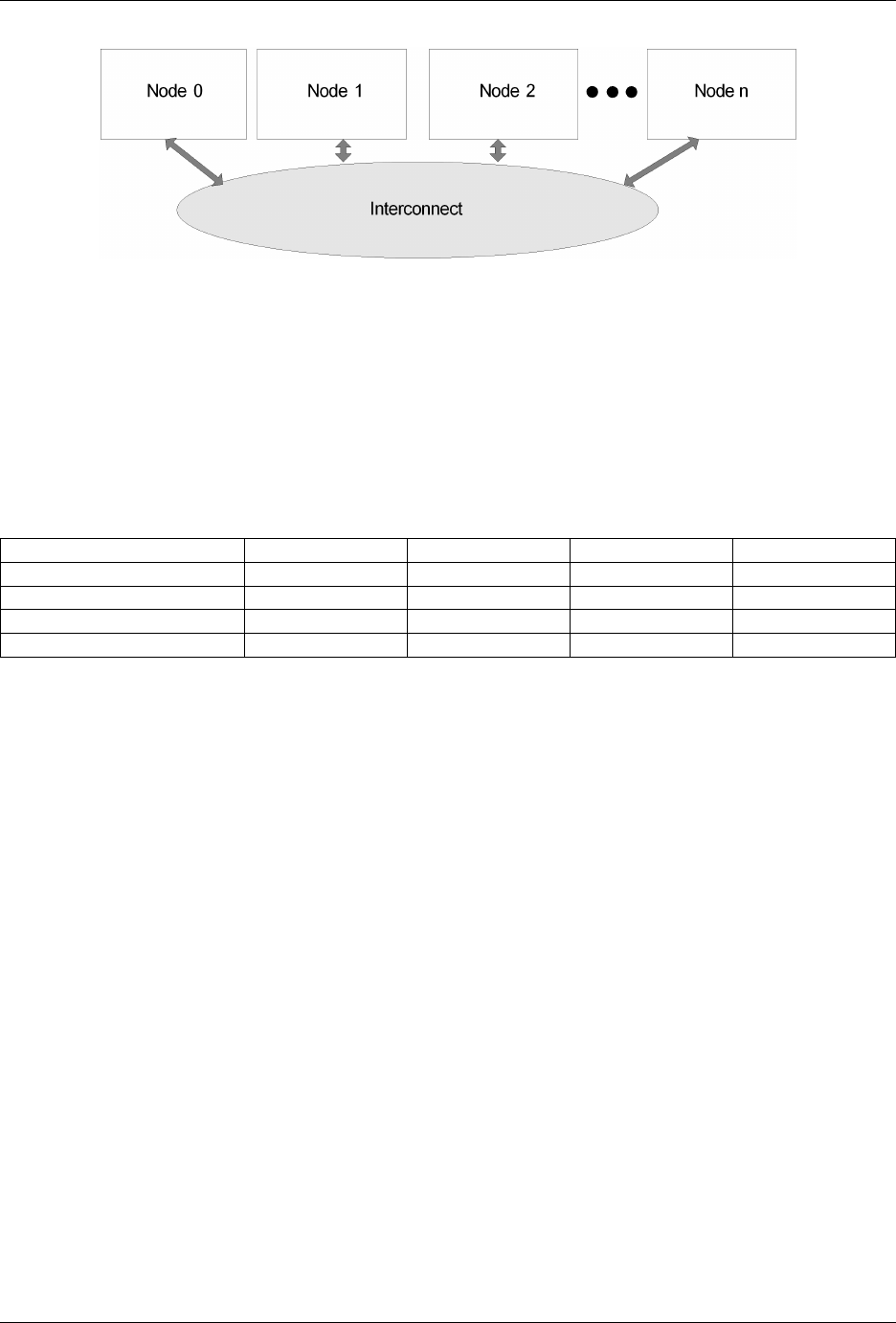
Advanced Configuration and Power Interface (ACPI) Specification, Release 6.5
Fig. 6.5: System Locality information Table
The System Locality Information Table diagrams a 4-node system where the nodes are numbered 0 through 3 (Node
n = Node 3) and the granularity is at the node level for the NUMA distance information. In this example we assign
System Localities / Proximity Domain numbers equal to the node numbers (0-3). The NUMA relative distances
between proximity domains as implemented in this system are described in the matrix represented in Example Relative
Distances Between Proximity Domains. Proximity Domains are represented by the numbers in the top row and left
column. Distances are represented by the values in cells internal in the table from the domains.
Table 6.17: Example Relative Distances Between Proximity Domains
ProximityDomain 0 1 2 3
0 10 15 20 18
1 15 10 16 24
2 20 16 10 12
3 18 24 12 10
6.2. Device Configuration Objects 371

Advanced Configuration and Power Interface (ACPI) Specification, Release 6.5
An example of these distances between proximity domains encoded in a System Locality Information Table for con-
sumption by OSPM at boot time is described in the table below.
Table 6.18: Example System Locality Information Table
Field Byte
Length
Byte
Offset
Description
Header
Signature 4 0 ‘SLIT’.
Length 4 4 60
Revision 1 8 1
Checksum 1 9 Entire table must sum to zero.
OEMID 6 10 OEM ID.
OEM Table ID 8 16 For the System Locality Information Table, the table ID
is the manufacturer model ID.
OEM Revision 4 24 OEM revision of System Locality Information Table for
supplied OEM Table ID.
Creator ID 4 28 Vendor ID of utility that created the table. For the
DSDT, RSDT, SSDT, and PSDT tables, this is the ID
for the ASL Compiler.
Creator Revision 4 32 Revision of utility that created the table. For the DSDT,
RSDT, SSDT, and PSDT tables, this is the revision for
the ASL Compiler.
Creator Revision
Number of System Localities 8 36 4
Entry[0][0] 1 44 10
Entry[0][1] 1 45 15
Entry[0][2] 1 46 20
Entry[0][3] 1 47 18
Entry[1][0] 1 48 15
Entry[1][1] 1 49 10
Entry[1][2] 1 50 16
Entry[1][3] 1 51 24
Entry[2][0] 1 52 20
Entry[2][1] 1 53 16
Entry[2][2] 1 54 10
Entry[2][3] 1 55 12
Entry[3][0] 1 56 18
Entry[3][1] 1 57 24
Entry[3][2] 1 58 12
Entry[3][3] 1 59 10
If a new “Node 4” is added, then the following table represents the updated system’s NUMA relative distances of
proximity domains.
6.2. Device Configuration Objects 372

Advanced Configuration and Power Interface (ACPI) Specification, Release 6.5
Table 6.19: Example Relative Distances Between Proximity Domains
- 5 Node
Proximity Domain 0 1 2 3 4
0 10 15 20 18 17
1 15 10 16 24 21
2 20 16 10 12 14
3 18 24 12 10 23
4 17 21 14 23 10
The new node’s _SLI object would evaluate to a buffer containing [17,21,14,23,10,17,21,14,23,10].
Note: Some systems support interleave memory across the nodes. The SLIT representation of these systems is
implementation specific.
6.2.16 _SRS (Set Resource Settings)
This optional control method takes one byte stream argument that specifies a new resource allocation for a device.
The resource descriptors in the byte stream argument must be specified exactly as listed in the _CRS byte stream -
meaning that the identical resource descriptors must appear in the identical order, resulting in a buffer of exactly the
same length. Optimizations such as changing an IRQ descriptor to an IRQNoFlags descriptor (or vice-versa) must not
be performed. Similarly, changing StartDependentFn to StartDependentFnNoPri is not allowed. A _CRS object can
be used as a template to ensure that the descriptors are in the correct format. For more information, see the _CRS
object definition.
The settings must take effect before the _SRS control method returns.
This method must not reference any operation regions that have not been declared available by a _REG method.
If the device is disabled, _SRS enables the device at the specified resources. _SRS is not used to disable a device; use
the _DIS control method instead.
Arguments: (1)
Arg0 - A Buffer containing a Resource Descriptor byte stream
Return Value:
None
6.2.17 _CCA (Cache Coherency Attribute)
The _CCA object returns whether or not a bus-master device supports hardware managed cache coherency. Expected
values are 0 to indicate it is not supported, and 1 to indicate that it is supported. All other values are reserved.
On platforms for which existing default cache-coherency behavior of the OS is not adequate, _CCA enables the OS to
adapt to the differences. If used, _CCA must be included under all bus-master-capable devices defined as children of
\_SB, to ensure that the operating system knows when it can rely on hardware managed cache coherency. The value
of _CCA is inherited by all descendants of these devices, so it need not be repeated for their children devices and will
be ignored by OSPM if it is provided there. This includes slave devices on a shared DMA controller; thus these DMA
controllers must also be defined in the namespace under the System Bus and include a _CCA object.
If a device indicates it does not have hardware cache coherency support, then OSPM must use a software cache flushing
algorithm to ensure stale or invalid data is not accessed from the caches.
6.2. Device Configuration Objects 373

Advanced Configuration and Power Interface (ACPI) Specification, Release 6.5
__CCA objects are only relevant for devices that can access CPU-visible memory, such as devices that are DMA
capable. On ARM based systems, the _CCA object must be supplied all such devices. On Intel platforms, if the _CCA
object is not supplied, the OSPM will assume the devices are hardware cache coherent.
Arguments:
None
Return Value:
An Integer indicating the device’s support for hardware cache coherency:
0 - The device does not have hardware managed cache coherency
1 - The device has hardware managed cache coherency
Other Values - Reserved
Note: There are restrictions related to when this object is evaluated which have implications for implementing this
object as a control method. The _CCA method must only access Operation Regions that have been indicated to be
available as defined by the _REG method. The _REG method is described in _REG (Region).
6.2.17.1 _CCA Example ASL:
Scope (\_SB) {
...
Device (XHCI) {
...
Name (_CCA, ZERO) // Cache-incoherent bus-master, child of \\_SB
...
}
...
Device (PCI0) { // Root PCI Bus
...
Name (_CCA, ONE) // Cache-coherent bus-master, child of \\_SB
...
Device (PRT0) {
... // Bus-master-capable, not a child of \\_SB
... // Will inherit coherency from PCI0, no \_CCA required
Device (NIC0) {
... // Bus-master-capable, not a child of \\_SB
... // Will inherit coherency from PRT0, no \_CCA required
}
}
}
...
Device (SDHC) {
...
Name (_CCA, ONE) // Cache-coherent bus-master-capable, child of \\_SB
...
}
...
Device (GPIO) {
... // Not bus-master-capable
... // \_CCA not valid
}
...
(continues on next page)
6.2. Device Configuration Objects 374

Advanced Configuration and Power Interface (ACPI) Specification, Release 6.5
(continued from previous page)
Device (DMAC) {
... // DMA controller; \_CCA must be specified
Name (_CCA, ONE) // Cache coherent bus-master, child of \\_SB
...
}
...
Device (SPI1) {
...
Name (_CRS, ResourceTemplate()
{
FixedDMA(...) // Sharing the DMA, thus inherits coherency from it
...
...
})
... // \_CCA not valid
}
}
6.2.18 _HMA(Heterogeneous Memory Attributes)
The Heterogeneous Memory Attributes Table (HMAT) defined in Heterogeneous Memory Attribute Table (HMAT)
provides Heterogeneous Memory Attributes. Dynamic runtime reconfiguration of the system may cause proximities
domains or memory attributes to change. If the “Reservation Hint” is set, new HMAT update shall not reset the
“Reservation Hint” unless the memory range is removed.
_HMA is an optional object that enables the platform to provide the OS with updated Heterogeneous Memory At-
tributes information at runtime. _HMA provides OSPM with the latest HMAT in entirety overriding existing HMAT.
Arguments:
None
Return Value:
A Buffer containing entire HMAT.
Example ASL for _HMA usage:
Scope (\_SB) {
Device (Dev1) {
...
}
Device (Dev2) {
...
}
Method (_HMA, 0) {
Return (HMAD)
}
} // end of \\_SB scope
6.2. Device Configuration Objects 375

Advanced Configuration and Power Interface (ACPI) Specification, Release 6.5
6.3 Device Insertion, Removal, and Status Objects
The objects defined in this section provide mechanisms for handling dynamic insertion and removal of devices and for
determining device and notification processing status.
Device insertion and removal objects are also used for docking and undocking mobile platforms to and from a pe-
ripheral expansion dock. These objects give information about whether or not devices are present, which devices are
physically in the same device (independent of which bus the devices live on), and methods for controlling ejection or
interlock mechanisms.
The system is more stable when removable devices have a software-controlled, VCR-style ejection mechanism instead
of a “surprise-style” ejection mechanism. In this system, the eject button for a device does not immediately remove
the device, but simply signals the operating system. OSPM then shuts down the device, closes open files, unloads the
driver, and sends a command to the hardware to eject the device.
1. If the device is physically inserted while the system is in the working state (in other words, hot insertion), the
hardware generates a general-purpose event.
2. The control method servicing the event uses the Notify(device,0) command to inform OSPM of the bus that the
new device is on or the device object for the new device. If the Notify command points to the device object for
the new device, the control method must have changed the device’s status returned by _STA to indicate that the
device is now present. The performance of this process can be optimized by having the object of the Notify as
close as possible, in the namespace hierarchy, to where the new device resides. The Notify command can also
be used from the _WAK control method (see Section 7.4.5) to indicate device changes that may have occurred
while the system was sleeping. For more information about the Notify command, see Section 5.6.6.
3. OSPM uses the identification and configuration objects to identify, configure, and load a device driver for the
new device and any devices found below the device in the hierarchy.
4. If the device has a _LCK control method, OSPM may later run this control method to lock the device.
The new device referred to in step 2 need not be a single device, but could be a whole tree of devices. For example, it
could point to the PCI-PCI bridge docking connector. OSPM will then load and configure all devices it found below
that bridge. The control method can also point to several different devices in the hierarchy if the new devices do not
all live under the same bus. (in other words, more than one bus goes through the connector).
For removing devices, ACPI supports both hot removal (system is in the S0 state), and warm removal (system is in a
sleep state: S1-S4). This is done using the _EJx control methods. Devices that can be ejected include an _EJx control
method for each sleeping state the device supports (a maximum of 2 _EJx objects can be listed). For example, hot
removal devices would supply an _EJ0; warm removal devices would use one of _EJ1-EJ4. These control methods
are used to signal the hardware when an eject is to occur.
The sequence of events for dynamically removing a device goes as follows:
1. The eject button is pressed and generates a general-purpose event. (If the system was in a sleeping state, it
should wake the system).
2. The control method for the event uses the Notify(device, 3) command to inform OSPM which specific device
the user has requested to eject. Notify does not need to be called for every device that may be ejected, but for
the top-level device. Any child devices in the hierarchy or any ejection-dependent devices on this device (as
described by _EJD, below) are automatically removed.
3. The OS shuts down and unloads devices that will be removed.
4. If the device has a _LCK control method, OSPM runs this control method to unlock the device.
5. The OS looks to see what _EJx control methods are present for the device. If the removal event will cause the
system to switch to battery power (in other words, an undock) and the battery is low, dead, or not present, OSPM
uses the lowest supported sleep state _EJx listed; otherwise it uses the highest state _EJx. Having made this
decision, OSPM runs the appropriate _EJx control method to prepare the hardware for eject.
6.3. Device Insertion, Removal, and Status Objects 376

Advanced Configuration and Power Interface (ACPI) Specification, Release 6.5
6. Warm removal requires that the system be put in a sleep state. If the removal will be a warm removal, OSPM
puts the system in the appropriate Sx state. If the removal will be a hot removal, OSPM skips to step 8, below.
7. For warm removal, the system is put in a sleep state. Hardware then uses any motors, and so on, to eject the
device. Immediately after ejection, the hardware transitions the system to S0. If the system was sleeping when
the eject notification came in, the OS returns the system to a sleeping state consistent with the user’s wake
settings.
8. OSPM calls _STA to determine if the eject successfully occurred. (In this case, control methods do not need to
use the Notify(device,3) command to tell OSPM of the change in _STA) If there were any mechanical failures,
_STA returns 3: device present and not functioning, and OSPM informs the user of the problem.
Note: This mechanism is the same for removing a single device and for removing several devices, as in an undock.
ACPI does not disallow surprise-style removal of devices; however, this type of removal is not recommended because
system and data integrity cannot be guaranteed when a surprise-style removal occurs. Because the OS is not informed,
its device drivers cannot save data buffers and it cannot stop accesses to the device before the device is removed. To
handle surprise-style removal, a general-purpose event must be raised. Its associated control method must use the
Notify command to indicate which bus the device was removed from.
The device insertion and removal objects are listed in the table below.
Table 6.20: Device Insertion, Removal, and Status Objects
Object Description
_EDL Object that evaluates to a package of namespace references of device objects that depend on the
device containing _EDL.
_EJD Object that evaluates to the name of a device object on which a device depends. Whenever the
named device is ejected, the dependent device must receive an ejection notification.
_EJx Control method that ejects a device.
_LCK Control method that locks or unlocks a device.
_OST Control method invoked by OSPM to convey processing status to the platform.
_RMV Object that indicates that the given device is removable.
_STA Control method that returns a device’s status.
6.3.1 _EDL (Eject Device List)
This object evaluates to a package of namespace references containing the names of device objects that depend on the
device under which the _EDL object is declared. This is primarily used to support docking stations. Before the device
under which the _EDL object is declared may be ejected, OSPM prepares the devices listed in the _EDL object for
physical removal.
Arguments:
None
Return Value:
A variable-length Package containing a list of namespace references
Before OSPM ejects a device via the device’s _EJx methods, all dependent devices listed in the package returned by
_EDL are prepared for removal. Notice that _EJx methods under the dependent devices are not executed.
When describing a platform that includes a docking station, an _EDL object is declared under the docking station
device. For example, if a mobile system can attach to two different types of docking stations, _EDL is declared under
6.3. Device Insertion, Removal, and Status Objects 377

Advanced Configuration and Power Interface (ACPI) Specification, Release 6.5
both docking station devices and evaluates to the packaged list of devices that must be ejected when the system is
ejected from the docking station.
An ACPI-compliant OS evaluates the _EDL method just prior to ejecting the device.
6.3.2 _EJD (Ejection Dependent Device)
This object is used to specify the name of a device on which the device, under which this object is declared, is
dependent. This object is primarily used to support docking stations. Before the device indicated by _EJD is ejected,
OSPM will prepare the dependent device (in other words, the device under which this object is declared) for removal.
Arguments:
None
Return Value:
A String containing the device name
_EJD is evaluated once when the ACPI table loads. The EJx methods of the device indicated by _EJD will be used to
eject all the dependent devices. A device’s dependents will be ejected when the device itself is ejected.
Note: OSPM will not execute a dependent device’s _EJx methods when the device indicated by _EJD is ejected.
When describing a platform that includes a docking station, usually more than one _EJD object will be needed. For
example, if a dock attaches both a PCI device and an ACPI-configured device to a mobile system, then both the PCI
device description package and the ACPI-configured device description package must include an _EJD object that
evaluates to the name of the docking station (the name specified in an _ADR or _HID object in the docking station’s
description package). Thus, when the docking connector signals an eject request, OSPM first attempts to disable and
unload the drivers for both the PCI and ACPI configured devices.
Note: An ACPI 1.0 OS evaluates the _EJD methods only once during the table load process. This greatly re-
stricts a table designer’s freedom to describe dynamic dependencies such as those created in scenarios with multiple
docking stations. This restriction is illustrated in the example below; the _EJD information supplied via and ACPI
1.0-compatible namespace omits the IDE2 device from DOCK2’s list of ejection dependencies. Starting in ACPI 2.0,
OSPM is presented with a more in-depth view of the ejection dependencies in a system by use of the _EDL methods.
Example
An example use of _EJD and _EDL is as follows:
Scope(\_SB.PCI0) {
Device(DOCK1) { // Pass through dock - DOCK1
Name(_ADR, ...)
Method(_EJ0, 0) {...}
Method(_DCK, 1) {...}
Name(_BDN, ...)
Method(_STA, 0) {0xF}
Name(_EDL, Package( ) { // DOCK1 has two dependent devices - IDE2 and CB2
\\_SB.PCI0.IDE2,
\\_SB.PCI0.CB2})
}
Device(DOCK2) { // Pass through dock - DOCK2
Name(_ADR, ...)
Method(_EJ0, 0) {...}
(continues on next page)
6.3. Device Insertion, Removal, and Status Objects 378

Advanced Configuration and Power Interface (ACPI) Specification, Release 6.5
(continued from previous page)
Method(_DCK, 1) {...}
Name(_BDN, ...)
Method(_STA, 0) {0x0}
Name(_EDL, Package( ) { // DOCK2 has one dependent device - IDE2
\\_SB.PCI0.IDE2})
}
Device(IDE1) { // IDE Drive1 not dependent on the dock
Name(_ADR, ...)
}
Device(IDE2) { // IDE Drive2
Name(_ADR, ...)
Name(_EJD,"\\_SB.PCI0.DOCK1") // Dependent on DOCK1
}
Device(CB2) { // CardBus Controller
Name(_ADR, ...)
Name(_EJD,"\\_SB.PCI0.DOCK1") // Dependent on DOCK1
}
} // end \\_SB.PCIO
6.3.3 _EJx (Eject)
These control methods are optional and are supplied for devices that support a software-controlled VCR-style ejection
mechanism or that require an action be performed such as isolation of power/data lines before the device can be
removed from the system. To support warm (system is in a sleep state) and hot (system is in S0) removal, an _EJx
control method is listed for each sleep state from which the device supports removal, where x is the sleeping state
supported. For example, _EJ0 indicates the device supports hot removal; _EJ1-EJ4 indicate the device supports warm
removal.
Arguments: (1)
Arg0 - An Integer containing a device ejection control
0 - Cancel a mark for ejection request (EJ0 will never be called with this value)
1 - Hot eject or mark for ejection
Return Value:
None
For hot removal, the device must be immediately ejected when OSPM calls the _EJ0 control method. The _EJ0 control
method does not return until ejection is complete. After calling _EJ0, OSPM verifies the device no longer exists to
determine if the eject succeeded. For _HID devices, OSPM evaluates the _STA method. For _ADR devices, OSPM
checks with the bus driver for that device.
For warm removal, the _EJ1-_EJ4 control methods do not cause the device to be immediately ejected. Instead, they
set proprietary registers to prepare the hardware to eject when the system goes into the given sleep state. The hardware
ejects the device only after OSPM has put the system in a sleep state by writing to the SLP_EN register. After the
system resumes, OSPM calls _STA to determine if the eject succeeded.
A device object may have multiple _EJx control methods. First, it lists an EJx control method for the preferred sleeping
state to eject the device. Optionally, the device may list an EJ4 control method to be used when the system has no
power (for example, no battery) after the eject. For example, a hot-docking notebook might list _EJ0 and _EJ4.
6.3. Device Insertion, Removal, and Status Objects 379

Advanced Configuration and Power Interface (ACPI) Specification, Release 6.5
6.3.4 _LCK (Lock)
This control method is optional and is required only for a device that supports a software-controlled locking mech-
anism. When the OS invokes this control method, the associated device is to be locked or unlocked based upon the
value of the argument that is passed. On a lock request, the control method must not complete until the device is
completely locked.
Arguments:
Arg0 - An Integer containing a device lock control
0 - Unlock the device
1 - Lock the device
Return Value:
None
When describing a platform, devices use either a _LCK control method or an _EJx control method for a device.
6.3.5 _OST (OSPM Status Indication)
This object is an optional control method that is invoked by OSPM to indicate processing status to the platform.
During device ejection, device hot add, Error Disconnect Recover, or other event processing, OSPM may need to
perform specific handshaking with the platform. OSPM may also need to indicate to the platform its inability to
complete a requested operation; for example, when a user presses an ejection button for a device that is currently
in use or is otherwise currently incapable of being ejected. In this case, the processing of the ACPI Eject Request
notification by OSPM fails. OSPM may indicate this failure to the platform through the invocation of the _OST control
method. As a result of the status notification indicating ejection failure, the platform may take certain action including
reissuing the notification or perhaps turning on an appropriate indicator light to signal the failure to the user.
Arguments: (3)
Arg0 - An Integer containing the source event
Arg1 - An Integer containing the status code
Arg2 - A Buffer containing status information
Return Value:
None
Argument Information:
Arg0 - source_event: DWordConst
If the value of source_event is <= 0xFF, this argument is the ACPI notification value whose processing generated the
status indication. This is the value that was passed into the Notify operator.
If the value of source_event is 0x100 or greater then the OSPM status indication is a result of an OSPM action as
indicated in OST Source Event Codes. For example, a value of 0x103 will be passed into _OST for this argument upon
the failure of a user interface invoked device ejection.
If OSPM is unable to identify the originating notification value, OSPM invokes _OST with a value that contains all
bits set (ones) for this parameter.
Arg1 – Status Code: DWordConst. OSPM indicates a notification value specific status. See Table 6.22, Table 6.23,
and Table 6.25 for status code descriptions.
Arg2 - A buffer containing detailed OSPM-specific information about the status indication. This argument may be
null.
6.3. Device Insertion, Removal, and Status Objects 380

Advanced Configuration and Power Interface (ACPI) Specification, Release 6.5
Table 6.21: OST Source Event Codes
Source Event
Code
Description
0-0xFF Reserved for Notification Values
0x100 Operation System Shutdown Processing
0x101-0x102 Reserved
0x103 Ejection Processing
0x104-0x1FF Reserved
0x200 Insertion Processing
0x201-
0xFFFFFFFF
Reserved
Table 6.22: General Processing Status Codes
Status Code Description
0 Success
1 Non-specific failure
2 Unrecognized Notify Code
3-0x7F Reserved
0x80-
0xFFFFFFFF
Notification value specific status codes
Table 6.23: Operating System Shutdown Processing (Source Events :
0x100) Status Codes
Status Code Description
0x80 OS Shutdown Request denied
0x81 OS Shutdown in progress
0x82 OS Shutdown completed
0x83 OS Graceful Shutdown not supported
0x84-
0xFFFFFFFF
Reserved
6.3.5.1 Processing Sequence for Graceful Shutdown Request:
Following receipt of the Graceful Shutdown Request (see Table 5.188, value 0x81), the OS will be responsible for
responding with one of the following status codes:
• 0x80 (OS Shutdown Request denied) - This value will be sent if the OS is not capable of performing a graceful
shutdown.
• 0x81 (OS Shutdown in progress) - The OS has initiated the graceful shutdown procedure.
• 0x83 (OS Graceful Shutdown not supported) - The OS does not support the Graceful Shutdown Request.
If the OS does initiate a graceful shutdown it should continue to generate the “OS Shutdown in progress” message
(_OST source event 0x100 status code 0x81) every 10 seconds. This functions as a heartbeat so that the service which
requested the graceful shutdown knows that the request is currently being processed. The platform should assume that
the OS shutdown is not proceeding if it does not receive the “OS Shutdown in progress” message for 60 seconds.
When the graceful shutdown procedure has completed the OSPM will send the “OS Shutdown completed” message
and then transition the platform to the G2 “soft-off” power state.
6.3. Device Insertion, Removal, and Status Objects 381

Advanced Configuration and Power Interface (ACPI) Specification, Release 6.5
Table 6.24: Ejection Request / Ejection Processing (Source Events:
0x03 and 0x103) Status Codes
Status Code Description
0x80 Device ejection not supported by OSPM
0x81 Device in use by application
0x82 Device Busy
0x83 Ejection dependency is busy or not supported for ejection by OSPM
0x84 Ejection is in progress (pending)
0x85-
0xFFFFFFFF
Reserved
Table 6.25: Insertion Processing (Source Event: 0x200) Status Codes
Status Code Description
0x80 Device insertion in progress (pending)
0x81 Device driver load failure
0x82 Device insertion not supported by OSPM
0x83-0x8F Reserved
0x90-0x9F Insertion failure - Resources Unavailable as described by the following bit encodings: Bit [3] Bus
or Segment Numbers Bit [2] Interrupts Bit [1] I/O Bit [0] Memory
0xA0-
0xFFFFFFFF
Reserved
It is possible for the platform to issue multiple notifications to OSPM and for OSPM to process the notifications
asynchronously. As such, OSPM may invoke _OST for notifications independent of the order the notification are
conveyed by the platform or by software to OSPM.
6.3. Device Insertion, Removal, and Status Objects 382

Advanced Configuration and Power Interface (ACPI) Specification, Release 6.5
The figure below provides and example event flow of device ejection on a platform employing the _OST object.
Fig. 6.6: Device Ejection Flow Example Using _OST
Note: To maintain compatibility with OSPM implementations of previous revisions of the ACPI specification, the
platform must not rely on OSPM’s evaluation of the _OST object for proper platform operation.
6.3. Device Insertion, Removal, and Status Objects 383

Advanced Configuration and Power Interface (ACPI) Specification, Release 6.5
Example ASL for _OST usage:
External (\_SB.PCI4, DeviceObj)
Scope(\_SB.PCI4) {
OperationRegion(LED1, SystemIO, 0x10C0, 0x20)
Field(LED1, AnyAcc, NoLock, Preserve)
{ // LED controls
S0LE, 1, // Slot 0 Ejection Progress LED
S0LF, 1, // Slot 0 Ejection Failure LED
S1LE, 1, // Slot 1 Ejection Progress LED
S1LF, 1, // Slot 1 Ejection Failure LED
S2LE, 1, // Slot 2 Ejection Progress LED
S2LF, 1, // Slot 2 Ejection Failure LED
S3LE, 1, // Slot 3 Ejection Progress LED
S3LF, 1 // Slot 3 Ejection Failure LED
}
Device(SLT3) { // hot plug device
Name(_ADR, 0x000C0003)
Method(_OST, 3, Serialized) { // OS calls \_OST with notify code 3 or 0x103
// and status codes 0x80-0x83
// to indicate a hot remove request failure.
// to indicate a hot remove request failure.
// Status code 0x84 indicates an ejection
// request pending.
If(LEqual(Arg0,Ones)) // Unspecified event
{
// Perform generic event processing here
}
Switch(And(Arg0,0xFF)) // Mask to retain low byte
{
Case(0x03) // Ejection request
{
Switch(Arg1)
{
Case(Package(){0x80, 0x81, 0x82, 0x83})
{ // Ejection Failure for some reason
Store(Zero, ^^S3LE) // Turn off Ejection Progress LED
Store(One, ^^S3LF) // Turn on Ejection Failure LED
}
Case(0x84) // Eject request pending
{
Store(One, ^^S3LE) // Turn on Ejection Request LED
Store(Zero, ^^S3LF) // Turn off Ejection Failure LED
}
}
}
}
} // end \_OST
Method(_EJ0, 1) // Successful ejection sequence
{
Store(Zero, ^^S3LE) // Turn off Ejection Progress LED
}
} // end SLT3
} // end scope \\_SB.PCI4
Scope (\_GPE)
{
Method(_E13)
{
(continues on next page)
6.3. Device Insertion, Removal, and Status Objects 384

Advanced Configuration and Power Interface (ACPI) Specification, Release 6.5
(continued from previous page)
Store(One, \\_SB.PCI4.S3LE) // Turn on ejection request LED
Notify(\_SB.PCI4.SLT3, 3) // Ejection request driven from GPE13
}
}
6.3.5.2 Processing Sequence for Error Disconnect Recover
If the OS attempts recovery operation following the receipt of the Error Disconnect Recover Request (see IPMI Status
Codes , value 0x0F) the OS will be responsible for invoking _OST with one of the following status codes in the lower
word of Arg1:
• 0x80 (Success) -This value will be sent if the OS successfully recovers all the child devices affected by Error
Disconnect Recover, reconfigures then and brings them back to functional state. All child devices are accessible
at the time _OST is evaluated.
• 0x81 (Not recovered) - The OS did not successfully recover one or more child devices that were affected by
Error Disconnect Recover. Access to the child devices affected by Error Disconnect Recover may be unreliable.
The upper word of Arg1 can be used to communicate bus-specific status information.
6.3.6 _RMV (Remove)
The optional _RMV object indicates to OSPM whether the device can be removed while the system is in the working
state and does not require any ACPI system firmware actions to be performed for the device to be safely removed from
the system (in other words, any device that only supports surprise-style removal). Any such removable device that
does not have _LCK or _EJx control methods must have an _RMV object. This allows OSPM to indicate to the user
that the device can be removed and to provide a way for shutting down the device before removing it. OSPM will
transition the device into D3 before telling the user it is safe to remove the device.
This method is reevaluated after a device-check notification.
Arguments:
None
Return Value:
An Integer containing the device removal status:
0 - The device cannot be removed
1 - The device can be removed
Note: Operating Systems implementing ACPI 1.0 interpret the presence of this object to mean that the device is
removable.
6.3. Device Insertion, Removal, and Status Objects 385

Advanced Configuration and Power Interface (ACPI) Specification, Release 6.5
6.3.7 _STA (Device Status)
This object returns the current status of a device, which can be one of the following: enabled, disabled, or removed.
OSPM evaluates the _STA object before it evaluates a device _INI method. The return values of the Present and Func-
tioning bits determines whether _INI should be evaluated and whether children of the device should be enumerated
and initialized. See _INI (Init). If _INI is not present within the scope of a Device, it is unspecified whether _STA is
evaluated prior to other objects within the Device scope.
Evaluation of _STA must not cause any change to platform context - it should be viewed as a “read only” operation.
If a device object describes a device that is not on an enumerable bus and the device object does not have an _STA
object, then OSPM assumes that the device is present, enabled, shown in the UI, and functioning.
This method must not reference any operation regions that have not been declared available by a _REG method.
Arguments:
None
Return Value:
An Integer containing a device status bitmap:
• Bit [0] - Set if the device is present.
• Bit [1] - Set if the device is enabled and decoding its resources.
• Bit [2] - Set if the device should be shown in the UI.
• Bit [3] - Set if the device is functioning properly (cleared if device failed its diagnostics).
• Bit [4] - Set if the battery is present.
• Bits [31:5] - Reserved (must be cleared).
Return Value Information
If bit [0] is cleared, then bit 1 must also be cleared (in other words, a device that is not present cannot be enabled).
A device can only decode its hardware resources if both bits 0 and 1 are set. If the device is not present (bit [0] cleared)
or not enabled (bit [1] cleared), then the device must not decode its resources.
If a device is present in the machine, but should not be displayed in OSPM user interface, bit 2 is cleared. For example,
a notebook could have joystick hardware (thus it is present and decoding its resources), but the connector for plugging
in the joystick requires a port replicator. If the port replicator is not plugged in, the joystick should not appear in the
UI, so bit [2] is cleared.
_STA may return bit 0 clear (not present) with bit [3] set (device is functional). This case is used to indicate a valid
device for which no device driver should be loaded (for example, a bridge device.) Children of this device may be
present and valid. OSPM should continue enumeration below a device whose _STA returns this bit combination.
Bit [4] of _STA applies only to the Control Method Battery Device (PNP0C0A). For all other devices, OSPM must
ignore this bit.
If a device object (including the processor object) does not have an _STA object, then OSPM assumes that all of the
above bits are set (i.e., the device is present, enabled, shown in the UI, and functioning).
If a device is present on an enumerable bus, then _STA must not return 0. In that case, bit[0] must be set and if
the status of the device can be determined through a bus-specific enumeration and discovery mechanism, it must be
reflected by the values of bit[1] and bit[3], even though the OSPM is not required to take them into account.
6.3. Device Insertion, Removal, and Status Objects 386

Advanced Configuration and Power Interface (ACPI) Specification, Release 6.5
6.4 Resource Data Types for ACPI
The _CRS, _PRS, and _SRS control methods use packages of resource descriptors to describe the resource require-
ments of devices.
6.4.1 ASL Macros for Resource Descriptors
ASL includes some macros for creating resource descriptors. The ASL syntax for these macros is defined in ASL
Operator Reference, along with the other ASL operators.
6.4.2 Small Resource Data Type
A small resource data type may be 2 to 8 bytes in size and adheres to the following format:
Table 6.26: Small Resource Data Type Tag Bit Definitions
Offset Field Description
Byte 0 Tag Bit [7]: Type-0 (Small item) || Tag Bits [6:3]: Small item name || Tag Bits [2:0]: Length- n
bytes
Bytes 1 to n Data bytes (Length 0 - 7)
The following small information items are currently defined for Plug and Play devices:
Table 6.27: Small Resource Items
Small Item Name Value
Reserved 0x00-0x03
IRQ Format Descriptor 0x04
DMA Format Descriptor 0x05
Start Dependent Functions Descriptor 0x06
End Dependent Functions Descriptor 0x07
I/O Port Descriptor 0x08
Fixed Location I/O Port Descriptor 0x09
Fixed DMA Descriptor 0x0A
Reserved 0x0B-0x0D
Vendor Defined Descriptor 0x0E
End Tag Descriptor 0x0F
6.4.2.1 IRQ Descriptor
Type 0, Small Item Name 0x4, Length = 2 or 3
The IRQ data structure indicates that the device uses an interrupt level and supplies a mask with bits set indicating the
levels implemented in this device. For standard PC-AT implementation there are 15 possible interrupts so a two-byte
field is used. This structure is repeated for each separate interrupt required.
Table 6.28: IRQ Descriptor Definition
Offset Field Name
Byte 0 Value = 0x22 or 0x23 (0010001nB) - Type = 0, Small item name = 0x4, Length = 2 or 3
Byte 1 IRQ mask bits[7:0], _INT Bit [0] represents IRQ0, bit[1] is IRQ1, and so on.
continues on next page
6.4. Resource Data Types for ACPI 387

Advanced Configuration and Power Interface (ACPI) Specification, Release 6.5
Table 6.28 – continued from previous page
Offset Field Name
Byte 2 IRQ mask bits[15:8], _INT Bit [0] represents IRQ8, bit[1] is IRQ9, and so on.
Byte 3
IRQ Information. Each bit, when set, indicates this device is capable of driving a certain type of
interrupt. (Optional–if not included then assume edge sensitive, high true interrupts.) These bits
can be used both for reporting and setting IRQ resources. Note: This descriptor is meant for
describing interrupts that are connected to PIC-compatible interrupt controllers, which can only
be programmed for Active-High-Edge-Triggered or Active-Low-Level-Triggered interrupts.
Any other combination is invalid. The Extended Interrupt Descriptor can be used to describe
other combinations:
Bit [7:6] Reserved (must be 0)
Bit [5] Wake Capability, _WKC
0x0 = Not Wake Capable: This interrupt is not capable of waking the system.
0x1 = Wake Capable: This interrupt is capable of waking the system from a low-power
idle state or a system sleep state.
Bit [4] Interrupt Sharing, _SHR
0x0 = Exclusive: This interrupt is not shared with other devices.
0x1 = Shared: This interrupt is shared with other devices.
Bit [3] Interrupt Polarity, _LL
0 Active-High - This interrupt is sampled when the signal is high, or true
1 Active-Low - This interrupt is sampled when the signal is low, or false.
Bit [2:1] Ignored
Bit [0] Interrupt Mode, _HE
0 Level-Triggered - Interrupt is triggered in response to signal in a low state.
1 Edge-Triggered - Interrupt is triggered in response to a change in signal state from low
to high.
Note: Low true, level sensitive interrupts may be electrically shared, but the process of how this might work is beyond
the scope of this specification.
Note: If byte 3 is not included, High true, edge sensitive, non-shareable is assumed.
See IRQ (Interrupt Resource Descriptor Macro) for a description of the ASL macros that create an IRQ descriptor.
6.4.2.2 DMA Descriptor
Type 0, Small Item Name 0x5, Length = 2
The DMA data structure indicates that the device uses a DMA channel and supplies a mask with bits set indicating the
channels actually implemented in this device. This structure is repeated for each separate channel required.
Table 6.29: DMA Descriptor Definition
Offset Field Name
Byte 0 Value = 0x2A (00101010B) - Type = 0, Small item name = 0x5, Length = 2
Byte 1 DMA channel mask bits [7:0] (channels 0 - 7), _DMA - Bit [0] is channel 0, etc.
continues on next page
6.4. Resource Data Types for ACPI 388

Advanced Configuration and Power Interface (ACPI) Specification, Release 6.5
Table 6.29 – continued from previous page
Byte 2
Bit [7] Reserved (must be 0)
Bits [6:5] DMA channel speed supported, _TYP:
00 Indicates compatibility mode
01 Indicates Type A DMA as described in the EISA
10 Indicates Type B DMA
11 Indicates Type F
Bits [4:3] Ignored
Bit [2] Logical device bus master status, _BM:
0 Logical device is not a bus master
1 Logical device is a bus master
Bits [1:0] DMA transfer type preference, _SIZ:
00 8-bit only
01 8- and 16-bit
10 16-bit only
11 Reserved
See DMA (DMA Resource Descriptor Macro) for a description of the ASL macro that creates a DMA descriptor.
6.4.2.3 Start Dependent Functions Descriptor
Type 0, Small Item Name 0x6, Length = 0 or 1
Each logical device requires a set of resources. This set of resources may have interdependencies that need to be
expressed to allow arbitration software to make resource allocation decisions about the logical device. Dependent
functions are used to express these interdependencies. The data structure definitions for dependent functions are
shown here. For a detailed description of the use of dependent functions refer to the next section.
Table 6.30: Start Dependent Functions Descriptor Definition
Offset Field Name
Byte 0
Value = 0x30 or 0x31 (0011000nB)
Type = 0, small item name = 0x6
Length = 0 or 1
Start Dependent Function fields may be of length 0 or 1 bytes. The extra byte is optionally used to denote the
compatibility or performance/robustness priority for the resource group following the Start DF tag. The compatibility
priority is a ranking of configurations for compatibility with legacy operating systems. This is the same as the priority
used in the PNPBIOS interface. For example, for compatibility reasons, the preferred configuration for COM1 is IRQ4,
I/O 3F8-3FF. The performance/robustness performance is a ranking of configurations for performance and robustness
reasons. For example, a device may have a high-performance, bus mastering configuration that may not be supported
by legacy operating systems. The bus-mastering configuration would have the highest performance/robustness priority
while its polled I/O mode might have the highest compatibility priority.
If the Priority byte is not included, this indicates the dependent function priority is ‘acceptable’. This byte is defined
as:
6.4. Resource Data Types for ACPI 389

Advanced Configuration and Power Interface (ACPI) Specification, Release 6.5
Table 6.31: Start Dependent Function Priority Byte Definition
Bits Definition
1:0
Compatibility priority. Acceptable values are:
0 Good configuration: Highest Priority and preferred configuration
1 Acceptable configuration: Lower Priority but acceptable configuration
2 Sub-optimal configuration: Functional configuration but not optimal
3 Reserved
3:2
Performance/robustness. Acceptable values are:
0 Good configuration: Highest Priority and preferred configuration
1 Acceptable configuration: Lower Priority but acceptable configuration
2 Sub-optimal configuration: Functional configuration but not optimal
3 Reserved
7:4 Reserved (must be 0)
Notice that if multiple Dependent Functions have the same priority, they are further prioritized by the order in which
they appear in the resource data structure. The Dependent Function that appears earliest (nearest the beginning) in the
structure has the highest priority, and so on.
See StartDependentFn (Start Dependent Function Resource Descriptor Macro) for a description of the ASL macro
that creates a Start Dependent Function descriptor.
6.4.2.4 End Dependent Functions Descriptor
Type 0, Small Item Name 0x7, Length = 0
Only one End Dependent Function item is allowed per logical device. This enforces the fact that Dependent Functions
cannot be nested.
Table 6.32: End Dependent Functions Descriptor Definition
Offset Field Name
Byte 0 Value = 0x38 (00111000B) - Type = 0, Small item name = 0x7, Length =0
See EndDependentFn (End Dependent Function Resource Descriptor Macro) for a description of the ASL macro that
creates an End Dependent Functions descriptor.
6.4.2.5 I/O Port Descriptor
Type 0, Small Item Name 0x8, Length = 7
There are two types of descriptors for I/O ranges. The first descriptor is a full function descriptor for programmable
devices. The second descriptor is a minimal descriptor for old ISA cards with fixed I/O requirements that use a 10-bit
ISA address decode. The first type descriptor can also be used to describe fixed I/O requirements for ISA cards that
require a 16-bit address decode. This is accomplished by setting the range minimum base address and range maximum
base address to the same fixed I/O value.
6.4. Resource Data Types for ACPI 390

Advanced Configuration and Power Interface (ACPI) Specification, Release 6.5
Table 6.33: I/O Port Descriptor Definition
Offset Field Name Definition
Byte 0 I/O Port Descriptor Value = 0x47 (01000111B) - Type = 0, Small item name =
0x8, Length = 7
Byte 1 Information Bits [7:1] Reserved and must be 0 Bit [0] (_DEC) 1 The logi-
cal device decodes 16-bit addresses 0 The logical device only
decodes address bits[9:0]
Byte 2 Range minimum base address, _MIN
bits[7:0]
Address bits [7:0] of the minimum base I/O address that the
card may be configured for.
Byte 3 Range minimum base address, _MIN
bits[15:8]
Address bits [15:8] of the minimum base I/O address that the
card may be configured for.
Byte 4 Range maximum base address,
_MAX bits[7:0]
Address bits [7:0] of the maximum base I/O address that the
card may be configured for.
Byte 5 Range maximum base address,
_MAX bits[15:8]
Address bits [15:8] of the maximum base I/O address that the
card may be configured for.
Byte 6 Base alignment, _ALN Alignment for minimum base address, increment in 1-byte
blocks.
Byte 7 Range length, _LEN The number of contiguous I/O ports requested.
See IO (IO Resource Descriptor Macro) for a description of the ASL macro that creates an I/O Port descriptor.
6.4.2.6 Fixed Location I/O Port Descriptor
Type 0, Small Item Name 0x9, Length = 3
This descriptor is used to describe 10-bit I/O locations.
Table 6.34: Fixed-Location I/O Port Descriptor Definition
Offset Field Name Definition
Byte 0 Fixed Location I/O Port Descriptor Value = 0x4B (01001011B) - Type = 0, Small item name =
0x9, Length = 3
Byte 1 Range base address, _BAS bits[7:0] Address bits [7:0] of the base I/O address that the card may be
configured for. This descriptor assumes a 10-bit ISA address
decode.
Byte 2 Range base address, _BAS bits[9:8] Address bits [9:8] of the base I/O address that the card may be
configured for. This descriptor assumes a 10-bit ISA address
decode.
Byte 3 Range length, _LEN The number of contiguous I/O ports requested.
See FixedIO (Fixed IO Resource Descriptor Macro) for a description of the ASL macro that creates a Fixed I/O Port
descriptor.
6.4. Resource Data Types for ACPI 391

Advanced Configuration and Power Interface (ACPI) Specification, Release 6.5
6.4.2.7 Fixed DMA Descriptor
Type 0, Small Item Name 0xA, Length = 5
The Fixed DMA descriptor provides a means for platforms to statically assign DMA request lines and channels to
devices connected to a shared DMA controller. This descriptor differs from the DMA descriptor in that it supports
many more DMA request lines and DMA controller channels, as well as a flexible mapping between the two. The
width of the bus used for transfers to the device is also provided. This structure is repeated for each separate request
line/channel pair required, and can only be used in the _CRS object. (Dynamic arbitration of Fixed DMA resource is
not supported.)
Table 6.35: Fixed DMA Resource Descriptor
Offset Field Name
Byte 0 Value = 0x55 (01010101B) - Type = 0, Small item name = 0xA, Length = 0x5
Byte 1 DMA Request Line bits [7:0] _DMA[7:0]. A platform-relative number uniquely identifying the
request line assigned. Request line-to-Controller mapping is done in a controller-specific OS
driver.
Byte 2 DMA Request Line bits [15:8] _DMA[15:8]
Byte 3 DMA Channel bits[7:0] _TYP[7:0]. A controller-relative number uniquely identifying the con-
troller’s logical channel assigned. Channel numbers can be shared by multiple request lines.
Byte 4 DMA Channel bits[15:8] _TYP[15:8]
Byte 5 DMA Transfer Width. _SIZ. Bus width that the device connected to this request line supports.
0x00 8-bit 0x01 16-bit 0x02 32-bit 0x03 64-bit 0x04 128-bit 0x05 256-bit 0x06-0xFF Reserved
6.4.2.8 Vendor-Defined Descriptor, Type 0
Type 0, Small Item Name 0xE, Length = 1 to 7
The vendor defined resource data type is for vendor use.
Table 6.36: Vendor-Defined Resource Descriptor Definition
Offset Field Name
Byte 0 Value = 0x71 - 0x77 (01110nnnB) - Type = 0, small item name = 0xE, Length = 1-7
Byte 1 to 7 Vendor defined
See VendorShort (Short Vendor Resource Descriptor) for a description of the ASL macro that creates a short vendor-
defined resource descriptor.
6.4.2.9 End Tag
Type 0, Small Item Name 0xF, Length = 1
The End tag identifies an end of resource data.
Note: If the checksum field is zero, the resource data is treated as if the checksum operation succeeded. Configuration
proceeds normally.
6.4. Resource Data Types for ACPI 392

Advanced Configuration and Power Interface (ACPI) Specification, Release 6.5
Table 6.37: End Tag Definition
Offset Field Name
Byte 0 Value = 0x79 (01111001B) - Type = 0, Small item name = 0xF, Length = 1
Byte 1 Checksum covering all resource data after the serial identifier. This checksum is generated such
that adding it to the sum of all the data bytes will produce a zero sum.
The End Tag is automatically generated by the ASL compiler at the end of the ResourceTemplate statement.
6.4.3 Large Resource Data Type
To allow for larger amounts of data to be included in the configuration data structure the large format is shown below.
This includes a 16-bit length field allowing up to 64 KB of data.
Table 6.38: Large Resource Data Type Tag Bit Definitions
Offset Field Name
Byte 0
Value = 1xxxxxxxB
Type = 1 (Large item)
Large item name = xxxxxxxB
Byte 1 Length of data items bits[7:0]
Byte 2 Length of data items bits[15:8]
Bytes 3 to (Length + 2) Actual data items
The following large information items are currently defined:
Table 6.39: Large Resource Items
Large Item Name Value
Reserved 0x00
24-Bit Memory Range Descriptor 0x01
Generic Register Descriptor 0x02
Reserved 0x03
Vendor-Defined Descriptor 0x04
32-Bit Memory Range Descriptor 0x05
32-Bit Fixed Memory Range Descriptor 0x06
Address Space Resource Descriptors 0x07
Word Address Space Descriptor 0x08
Extended Interrupt Descriptor 0x09
QWord Address Space Descriptor 0x0A
Extended Address Space Descriptor 0x0B
GPIO Connection Descriptor 0x0C
Pin Function Descriptor 0x0D
GenericSerialBus Connection Descriptors 0x0E
Pin Configuration Descriptor 0x0F
Pin Group Descriptor 0x10
Pin Group Function Descriptor 0x11
Pin Group Configuration Descriptor 0x12
Clock Input Resource Descriptor 0x13
Reserved 0x14-0x7F
6.4. Resource Data Types for ACPI 393

Advanced Configuration and Power Interface (ACPI) Specification, Release 6.5
6.4.3.1 24-Bit Memory Range Descriptor
Type 1, Large Item Value 0x1
The 24-bit memory range descriptor describes a device’s memory range resources within a 24-bit address space
Table 6.40: 24-bit Memory Range Descriptor Definition
Offset Field Name, ASL Field Name Definition
Byte 0 24-bit Memory Range Descriptor Value = 0x81 (10000001B) - Type = 1, Large item name =
0x01
Byte 1 Length, bits[7:0] Value = 0x09 (9)
Byte 2 Length, bits[15:8] Value = 0x00
Byte 3 Information
This field provides extra information about this memory:
Bit [7:1] Ignored
Bit [0] Write status, _RW:
1 writeable (read/write)
0 non-writeable (read-only)
Byte 4 Range minimum base address, _MIN,
bits[7:0]
Address bits [15:8] of the minimum base memory address for
which the card may be configured.
Byte 5 Range minimum base address, _MIN,
bits[15:8]
Address bits [23:16] of the minimum base memory address
for which the card may be configured
Byte 6 Range maximum base address,
_MAX, bits[7:0]
Address bits [15:8] of the maximum base memory address for
which the card may be configured.
Byte 7 Range maximum base address,
_MAX, bits[15:8]
Address bits [23:16] of the maximum base memory address
for which the card may be configured
Byte 8 Base alignment, _ALN, bits[7:0] This field contains the lower eight bits of the base alignment.
The base alignment provides the increment for the minimum
base address. (0x0000 = 64 KB)
Byte 9 Base alignment, _ALN, bits[15:8] This field contains the upper eight bits of the base alignment.
The base alignment provides the increment for the minimum
base address. (0x0000 = 64 KB)
Byte 10 Range length, _LEN, bits[7:0] This field contains the lower eight bits of the memory range
length. The range length provides the length of the memory
range in 256 byte blocks.
Byte 11 Range length, _LEN, bits[15:8] This field contains the upper eight bits of the memory range
length. The range length field provides the length of the mem-
ory range in 256 byte blocks.
Note: Address bits [7:0] of memory base addresses are assumed to be 0.
Note: A Memory range descriptor can be used to describe a fixed memory address by setting the range minimum
base address and the range maximum base address to the same value.
Note: 24-bit Memory Range descriptors are used for legacy devices.
6.4. Resource Data Types for ACPI 394

Advanced Configuration and Power Interface (ACPI) Specification, Release 6.5
Note: Mixing of 24-bit and 32-bit memory descriptors on the same device is not allowed.
See Memory24 (Memory Resource Descriptor Macro) for a description of the ASL macro that creates a 24-bit Memory
descriptor.
6.4.3.2 Vendor-Defined Descriptor, Type 1
Type 1, Large Item Value 0x4
The vendor defined resource data type is for vendor use.
Table 6.41: Large Vendor-Defined Resource Descriptor Definition
Offset Field Name Definition
Byte 0 Vendor Defined Descriptor Value = 0x84 (10000100B) - Type = 1, Large item name =
0x04
Byte 1 Length, bits [7:0] Lower eight bits of data length (UUID and vendor data)
Byte 2 Length, bits [15:8] Upper eight bits of data length (UUID and vendor data)
Byte 3 UUID specific descriptor sub
type
UUID specific descriptor sub type value
Byte 4-19 UUID UUID Value
Byte 20-
(Length+20)
Vendor Defined Data Vendor defined data bytes
This specification (ACPI) defines the UUID specific descriptor subtype field and the UUID field to address potential
collision of the use of this descriptor. It is strongly recommended that all newly defined vendor descriptors use these
fields prior to Vendor Defined Data.
See VendorLong for a description of the ASL macro that creates a long vendor-defined resource descriptor.
6.4.3.3 32-Bit Memory Range Descriptor
Type 1, Large Item Value 0x5
This memory range descriptor describes a device’s memory resources within a 32-bit address space.
Table 6.42: 32-Bit Memory Range Descriptor Definition
Offset Field Name Definition
Byte 0 32-bit Memory Range Descrip-
tor
Value = 0x85 (10000101B) - Type = 1, Large item name =
0x05
Byte 1 Length, bits [7:0] Value = 0x11 (17)
Byte 2 Length, bits [15:8] Value = 0x00
Byte 3 Information
This field provides extra information about this memory:
Bit [7:1] Ignored
Bit [0] Write status, _RW:
1 writeable (read/write)
0 non-writeable (read-only)
continues on next page
6.4. Resource Data Types for ACPI 395

Advanced Configuration and Power Interface (ACPI) Specification, Release 6.5
Table 6.42 – continued from previous page
Byte 4 Range minimum base address,
_MIN, bits [7:0]
Address bits [7:0] of the minimum base memory address for
which the card may be configured.
Byte 5 Range minimum base address,
_MIN, bits [15:8]
Address bits [15:8] of the minimum base memory address for
which the card may be configured.
Byte 6 Range minimum base address,
_MIN, bits [23:16]
Address bits [23:16] of the minimum base memory address
for which the card may be configured.
Byte 7 Range minimum base address,
_MIN, bits [31:24]
Address bits [31:24] of the minimum base memory address
for which the card may be configured.
Byte 8 Range maximum base address,
_MAX, bits [7:0]
Address bits [7:0] of the maximum base memory address for
which the card may be configured.
Byte 9 Range maximum base address,
_MAX, bits [15:8]
Address bits [15:8] of the maximum base memory address for
which the card may be configured.
Byte 10 Range maximum base address,
_MAX, bits [23:16]
Address bits [23:16] of the maximum base memory address
for which the card may be configured.
Byte 11 Range maximum base address,
_MAX, bits [31:24]
Address bits [31:24] of the maximum base memory address
for which the card may be configured.
Byte 12 Base alignment, _ALN bits
[7:0]
This field contains bits [7:0] of the base alignment. The base
alignment provides the increment for the minimum base ad-
dress.
Byte 13 Base alignment, _ALN bits
[15:8]
This field contains bits [15:8] of the base alignment. The base
alignment provides the increment for the minimum base ad-
dress.
Byte 14 Base alignment, _ALN bits
[23:16]
This field contains bits [23:16] of the base alignment. The
base alignment provides the increment for the minimum base
address.
Byte 15 Base alignment, _ALN bits
[31:24]
This field contains bits [31:24] of the base alignment. The
base alignment provides the increment for the minimum base
address.
Byte 16 Range length, _LEN bits [7:0] This field contains bits [7:0] of the memory range length. The
range length provides the length of the memory range in 1-
byte blocks.
Byte 17 Range length, _LEN bits [15:8] This field contains bits [15:8] of the memory range length.
The range length provides the length of the memory range in
1-byte blocks.
Byte 18 Range length, _LEN bits
[23:16]
This field contains Bits [23:16] of the memory range length.
The range length provides the length of the memory range in
1-byte blocks.
Byte 19 Range length, _LEN bits
[31:24]
This field contains Bits [31:24] of the memory range length.
The range length provides the length of the memory range in
1-byte blocks.
Note: Mixing of 24-bit and 32-bit memory descriptors on the same device is not allowed.
See Memory32 (Memory Resource Descriptor Macro) for a description of the ASL macro that creates a 32-bit Memory
descriptor.
6.4. Resource Data Types for ACPI 396

Advanced Configuration and Power Interface (ACPI) Specification, Release 6.5
6.4.3.4 32-Bit Fixed Memory Range Descriptor
Type 1, Large Item Value 0x6
This memory range descriptor describes a device’s memory resources within a 32-bit address space.
Table 6.43: 32-bit Fixed-Location Memory Range Descriptor Defini-
tion
Offset Field Name Definition
Byte 0 32-bit Fixed Memory Range Descriptor Value = 0x86 (10000110B) - Type = 1, Large item name
= 0x06
Byte 1 Length, bits [7:0] Value = 0x09 (9)
Byte 2 Length, bits [15:8] Value = 0x00
Byte 3 Information This field provides extra information about this memory.
Bit [7:1] Ignored Bit [0] Write status, _RW 1 writeable
(read/write) 0 non-writeable (read-only))
Byte 4 Range base address, _BAS bits [7:0] Address bits [7:0] of the base memory address for which
the card may be configured.
Byte 5 Range base address, _BAS bits [15:8] Address bits [15:8] of the base memory address for
which the card may be configured.
Byte 6 Range base address, _BAS bits [23:16] Address bits [23:16] of the base memory address for
which the card may be configured.
Byte 7 Range base address, _BAS bits [31:24] Address bits [31:24] of the base memory address for
which the card may be configured.
Byte 8 Range length, _LEN bits [7:0] This field contains bits [7:0] of the memory range
length. The range length provides the length of the
memory range in 1-byte blocks.
Byte 9 Range length, _LEN bits[15:8] This field contains bits [15:8] of the memory range
length. The range length provides the length of the
memory range in 1-byte blocks.
Byte 10 Range length, _LEN bits [23:16] This field contains bits [23:16] of the memory range
length. The range length provides the length of the
memory range in 1-byte blocks.
Byte 11 Range length, _LEN bits [31:24] This field contains bits [31:24] of the memory range
length. The range length provides the length of the
memory range in 1-byte blocks.
Note: Mixing of 24-bit and 32-bit memory descriptors on the same device is not allowed.
See Memory32Fixed (Memory Resource Descriptor Macro) for a description of the ASL macro that creates a 32-bit
Fixed Memory descriptor.
6.4. Resource Data Types for ACPI 397

Advanced Configuration and Power Interface (ACPI) Specification, Release 6.5
6.4.3.5 Address Space Resource Descriptors
The QWORD, DWORD, WORD, and Extended Address Space Descriptors are general-purpose structures for de-
scribing a variety of types of resources. These resources also include support for advanced server architectures (such
as multiple root buses), and resource types found on some RISC processors. These descriptors can describe various
kinds of resources. The following table defines the valid combination of each field and how they should be interpreted.
Table 6.44: Valid Combination of Address Space Descriptor Fields
_LEN _MIF _MAF Definition
0 0 0 Variable size, variable location resource descriptor for _PRS.
If _MIF is set, _MIN must be a multiple of (_GRA+1). If _MAF is set, _MAX
must be (a multiple of (_GRA+1))-1.
OS can pick the resource range that satisfies following conditions:
If _MIF is not set, start address is a multiple of (_GRA+1) and greater or equal
to _MIN. Otherwise, start address is _MIN.
If _MAF is not set, end address is (a multiple of (_GRA+1))-1 and less or equal
to _MAX. Otherwise, end address is _MAX.
0 0 1 Variable size, variable location resource descriptor for _PRS.
If _MIF is set, _MIN must be a multiple of (_GRA+1). If _MAF is set, _MAX
must be (a multiple of (_GRA+1))-1.
OS can pick the resource range that satisfies following conditions:
If _MIF is not set, start address is a multiple of (_GRA+1) and greater or equal
to _MIN. Otherwise, start address is _MIN.
If _MAF is not set, end address is (a multiple of (_GRA+1))-1 and less or equal
to _MAX. Otherwise, end address is _MAX.
0 1 0 Variable size, variable location resource descriptor for _PRS.
If _MIF is set, _MIN must be a multiple of (_GRA+1). If _MAF is set, _MAX
must be (a multiple of (_GRA+1))-1.
OS can pick the resource range that satisfies following conditions:
If _MIF is not set, start address is a multiple of (_GRA+1) and greater or equal
to _MIN. Otherwise, start address is _MIN.
If _MAF is not set, end address is (a multiple of (_GRA+1))-1 and less or equal
to _MAX. Otherwise, end address is _MAX.
0 1 1 (Invalid combination)
> 0 0 0 Fixed size, variable location resource descriptor for _PRS.
_LEN must be a multiple of (_GRA+1).
OS can pick the resource range that satisfies following conditions:
Start address is a multiple of (_GRA+1) and greater or equal to _MIN.
End address is (start address+_LEN-1) and less or equal to _MAX.
> 0 0 1 (Invalid combination)
> 0 1 0 (Invalid combination)
> 0 1 1 Fixed size, fixed location resource descriptor.
_GRA must be 0 and _LEN must be (_MAX - _MIN +1).
6.4. Resource Data Types for ACPI 398

Advanced Configuration and Power Interface (ACPI) Specification, Release 6.5
6.4.3.5.1 QWord Address Space Descriptor
Type 1, Large Item Value 0xA
The QWORD address space descriptor is used to report resource usage in a 64-bit address space (like memory and
I/O).
Table 6.45: WORD Address Space Descriptor Definition
Offset Field Name Definition
Byte 0 QWORD Address Space
Descriptor
Value = 0x8A (10001010B) - Type = 1, Large item name = 0x0A
Byte 1 Length, bits[7:0] Variable length, minimum value = 0x2B (43)
Byte 2 Length, bits[15:8] Variable length, minimum value = 0x00
Byte 3 Resource Type Indicates which type of resource this descriptor describes. Defined values
are: 0 Memory range 1 I/O range 2 Bus number range 3-191 Reserved
192-255 Hardware Vendor Defined
Byte 4 General Flags
Flags that are common to all resource types:
Bits [7:4] Reserved (must be 0)
Bit [3] Max Address Fixed, _MAF:
1 The specified maximum address is fixed
0 The specified maximum address is not fixed and can be changed
Bit [2] Min Address Fixed,_MIF:
1 The specified minimum address is fixed
0 The specified minimum address is not fixed and can be changed
Bit [1] Decode Type, _DEC:
1 This bridge subtractively decodes this address (top level bridges
only)
0 This bridge positively decodes this address Bit [0] Ignored
Byte 5 Type Specific Flags Flags that are specific to each resource type. The meaning of the flags in
this field depends on the value of the Resource Type field (see above).
Byte 6 Address space granularity,
_GRA bits[7:0]
A set bit in this mask means that this bit is decoded. All bits less signifi-
cant than the most significant set bit must be set. That is, the value of the
full Address Space Granularity field (all 64 bits) must be a number (2n-1).
Byte 7 Address space granularity,
_GRA bits[15:8]
Byte 8 Address space granularity,
_GRA bits[23:16]
Byte 9 Address space granularity,
_GRA bits[31:24]
Byte 10 Address space granularity,
_GRA bits[39:32]
Byte 11 Address space granularity,
_GRA bits[47:40]
Byte 12 Address space granularity,
_GRA bits[55:48]
Byte 13 Address space granularity,
_GRA bits[63:56]
Byte 14 Address range minimum,
_MIN bits[7:0]
For bridges that translate addresses, this is the address space on the sec-
ondary side of the bridge.
continues on next page
6.4. Resource Data Types for ACPI 399

Advanced Configuration and Power Interface (ACPI) Specification, Release 6.5
Table 6.45 – continued from previous page
Offset Field Name Definition
Byte 15 Address range minimum,
_MIN bits[15:8]
Byte 16 Address range minimum,
_MIN bits[23:16]
Byte 17 Address range minimum,
_MIN bits[31:24]
Byte 18 Address range minimum,
_MIN bits[39:32]
Byte 19 Address range minimum,
_MIN bits[47:40]
Byte 20 Address range minimum,
_MIN bits[55:48]
Byte 21 Address range minimum,
_MIN bits[63:56]
Byte 22 Address range maximum,
_MAX bits[7:0]
For bridges that translate addresses, this is the address space on the sec-
ondary side of the bridge.
Byte 23 Address range maximum,
_MAX bits[15:8]
Byte 24 Address range maximum,
_MAX bits[23:16]
Byte 25 Address range maximum,
_MAX bits[31:24]
Byte 26 Address range maximum,
_MAX bits[39:32]
For bridges that translate addresses, this is the address space on the sec-
ondary side of the bridge.
Byte 27 Address range maximum,
_MAX bits[47:40]
Byte 28 Address range maximum,
_MAX bits[55:48]
Byte 29 Address range maximum,
_MAX bits[63:56]
Byte 30 Address Translation off-
set, _TRA bits[7:0]
For bridges that translate addresses across the bridge, this is the offset
that must be added to the address on the secondary side to obtain the ad-
dress on the primary side. Non-bridge devices must list 0 for all Address
Translation offset bits.
Byte 31 Address Translation off-
set, _TRA bits[15:8]
Byte 32 Address Translation off-
set, _TRA bits[23:16]
Byte 33 Address Translation off-
set, _TRA bits[31:24]
Byte 34 Address Translation off-
set, _TRA bits[39:32]
Byte 35 Address Translation off-
set, _TRA bits[47:40]
Byte 36 Address Translation off-
set, _TRA bits[55:48]
Byte 37 Address Translation off-
set, _TRA bits[63:56]
Byte 38 Address length, _LEN
bits[7:0]
continues on next page
6.4. Resource Data Types for ACPI 400

Advanced Configuration and Power Interface (ACPI) Specification, Release 6.5
Table 6.45 – continued from previous page
Offset Field Name Definition
Byte 39 Address length, _LEN,
bits[15:8]
Byte 40 Address length, _LEN
bits[23:16]
Byte 41 Address length, _LEN
bits[31:24]
Byte 42 Address length, _LEN
bits[39:32]
Byte 43 Address length, _LEN
bits[47:40]
Byte 44 Address length, _LEN
bits[55:48]
Byte 45 Address length, _LEN
bits[63:56]
Byte 46 Resource Source Index Reserved. If the platform specifies “Interrupt ResourceSource support”
in bit 13 of Platform-Wide _OSC Capabilities DWORD 2, then this field
must be zero.
String Resource Source (Optional) If present, the device that uses this descriptor consumes its
resources from the resources produced by the named device object. If not
present, the device consumes its resources out of a global pool.
See QWordIO, QWordMemory, and ASL_QWordAddressSpace for a description of the ASL macros that creates a
QWORD Address Space descriptor.
6.4.3.5.2 DWord Address Space Descriptor
Type 1, Large Item Value 0x7
The DWORD address space descriptor is used to report resource usage in a 32-bit address space (like memory and
I/O).
Table 6.46: DWORD Address Space Descriptor Definition
Offset Field Name Definition
Byte 0 DWORD Address Space
Descriptor
Value = 0x87 (10000111B) - Type = 1, Large item name = 0x07
Byte 1 Length, bits [7:0] Variable: Value = 23 (minimum)
Byte 2 Length, bits [15:8] Variable: Value = 0 (minimum)
Byte 3 Resource Type
Indicates which type of resource this descriptor describes. Defined
values are:
0 Memory range
1 I/O range
2 Bus number range
3-191 Reserved
192-255 Hardware Vendor Defined
continues on next page
6.4. Resource Data Types for ACPI 401

Advanced Configuration and Power Interface (ACPI) Specification, Release 6.5
Table 6.46 – continued from previous page
Byte 4 General Flags
Flags that are common to all resource types:
Bits [7:4] Reserved (must be 0)
Bit [3] Max Address Fixed, _MAF:
1 The specified maximum address is fixed
0 The specified maximum address is not fixed and can be changed
Bit [2] Min Address Fixed,_MIF:
1 The specified minimum address is fixed
0 The specified minimum address is not fixed and can be changed
Bit [1] Decode Type, _DEC:
1 This bridge subtractively decodes this address (top level bridges
only)
0 This bridge positively decodes this address
Bit [0] Ignored
Byte 5 Type Specific Flags Flags that are specific to each resource type. The meaning of the flags in
this field depends on the value of the Resource Type field (see above).
Byte 6 Address space granularity,
_GRA bits[7:0]
A set bit in this mask means that this bit is decoded. All bits less signif-
icant than the most significant set bit must be set. (in other words, the
value of the full Address Space Granularity field (all 32 bits) must be a
number (2n-1).
Byte 7 Address space granularity,
_GRA bits[15:8]
Byte 8 Address space granularity,
_GRA bits [23:16]
Byte 9 Address space granularity,
_GRA bits [31:24]
Byte 10 Address range minimum,
_MIN bits [7:0]
For bridges that translate addresses, this is the address space on the sec-
ondary side of the bridge.
Byte 11 Address range minimum,
_MIN bits [15:8]
Byte 12 Address range minimum,
_MIN bits [23:16]
Byte 13 Address range minimum,
_MIN bits [31:24]
Byte 14 Address range maximum,
_MAX bits [7:0]
For bridges that translate addresses, this is the address space on the sec-
ondary side of the bridge.
Byte 15 Address range maximum,
_MAX bits [15:8]
Byte 16 Address range maximum,
_MAX bits [23:16]
Byte 17 Address range maximum,
_MAX bits [31:24]
Byte 18 Address Translation off-
set, _TRA bits [7:0]
For bridges that translate addresses across the bridge, this is the offset
that must be added to the address on the secondary side to obtain the ad-
dress on the primary side. Non-bridge devices must list 0 for all Address
Translation offset bits.
Byte 19 Address Translation off-
set, _TRA bits [15:8]
continues on next page
6.4. Resource Data Types for ACPI 402

Advanced Configuration and Power Interface (ACPI) Specification, Release 6.5
Table 6.46 – continued from previous page
Byte 20 Address Translation off-
set, _TRA bits [23:16]
Byte 21 Address Translation off-
set, _TRA bits [31:24]
Byte 22 Address Length, _LEN,
bits [7:0]
Byte 23 Address Length, _LEN,
bits [15:8]
Byte 24 Address Length, _LEN,
bits [23:16]
Byte 25 Address Length, _LEN,
bits [31:24]
Byte 26 Resource Source Index (Optional) Only present if Resource Source (below) is present. This field
gives an index to the specific resource descriptor that this device consumes
from in the current resource template for the device object pointed to in
Resource Source.
String Resource Source (Optional) If present, the device that uses this descriptor consumes its
resources from the resources produced by the named device object. If not
present, the device consumes its resources out of a global pool. If not
present, the device consumes this resource from its hierarchical parent.
See DWordIO, DWordMemory and ASL_DWordAddressSpace for a description of the ASL macro that creates a
DWORD Address Space descriptor
6.4.3.5.3 Word Address Space Descriptor
Type 1, Large Item Value 0x8
The WORD address space descriptor is used to report resource usage in a 16-bit address space (like memory and I/O).
Note: This descriptor is exactly the same as the DWORD descriptor specified in End Dependent Functions Descrip-
tor; the only difference is that the address fields are 16 bits wide rather than 32 bits wide.
Table 6.47: WORD Address Space Descriptor Definition
Offset Field Name Definition
Byte 0 WORD Address Space
Descriptor
Value = 0x88 (10001000B) - Type = 1, Large item name = 0x08
Byte 1 Length, bits [7:0] Variable length, minimum value = 0x0D (13)
Byte 2 Length, bits [15:8] Variable length, minimum value = 0x00
Byte 3 Resource Type
Indicates which type of resource this descriptor describes. Defined
values are:
0 Memory range
1 I/O range
2 Bus number range
3-191 Reserved
192-255 Hardware Vendor Defined
continues on next page
6.4. Resource Data Types for ACPI 403

Advanced Configuration and Power Interface (ACPI) Specification, Release 6.5
Table 6.47 – continued from previous page
Offset Field Name Definition
Byte 4 General Flags
Flags that are common to all resource types:
Bit [3] Max Address Fixed, _MAF:
1 The specified maximum address is fixed
0 The specified maximum address is not fixed and can be changed
Bit [2] Min Address Fixed,_MIF:
1 The specified minimum address is fixed
0 The specified minimum address is not fixed and can be changed
Bit [1] Decode Type, _DEC:
1 This bridge subtractively decodes this address (top level bridges
only)
0 This bridge positively decodes this address
Bit [0] Ignored
Byte 5 Type Specific Flags Flags that are specific to each resource type. The meaning of the flags in
this field depends on the value of the Resource Type field (see above).
Byte 6 Address space granularity,
_GRA bits[7:0]
A set bit in this mask means that this bit is decoded. All bits less signif-
icant than the most significant set bit must be set. (In other words, the
value of the full Address Space Granularity field (all 16 bits) must be a
number (2n-1).
Byte 7 Address space granularity,
_GRA bits[15:8]
Byte 8 Address range minimum,
_MIN, bits [7:0]
For bridges that translate addresses, this is the address space on the sec-
ondary side of the bridge.
Byte 9 Address range minimum,
_MIN, bits [15:8]
Byte 10 Address range maximum,
_MAX, bits [7:0]
For bridges that translate addresses, this is the address space on the sec-
ondary side of the bridge.
Byte 11 Address range maximum,
_MAX, bits [15:8]
Byte 12 Address Translation off-
set, _TRA, bits [7:0]
For bridges that translate addresses across the bridge, this is the offset
that must be added to the address on the secondary side to obtain the ad-
dress on the primary side. Non-bridge devices must list 0 for all Address
Translation offset bits.
Byte 13 Address Translation off-
set, _TRA, bits [15:8]
Byte 14 Address Length, _LEN,
bits [7:0]
Byte 15 Address Length, _LEN,
bits [15:8]
Byte 16 Resource Source Index (Optional) Only present if Resource Source (below) is present. This field
gives an index to the specific resource descriptor that this device consumes
from in the current resource template for the device object pointed to in
Resource Source.
String Resource Source (Optional) If present, the device that uses this descriptor consumes its
resources from the resources produced by the named device object. If not
present, the device consumes its resources out of a global pool. If not
present, the device consumes this resource from its hierarchical parent.
See WordIO, WordBusNumber, and ASL_WordAddressSpace for a description of the ASL macros that create a Word
6.4. Resource Data Types for ACPI 404

Advanced Configuration and Power Interface (ACPI) Specification, Release 6.5
address descriptor.
6.4.3.5.4 Extended Address Space Descriptor
Type 1, Large Item Value 0xB
The Extended Address Space descriptor is used to report resource usage in the address space (like memory and I/O).
Table 6.48: Extended Address Space Descriptor Definition
Offset Field Name Definition
Byte 0 Extended Address Space
Descriptor
Value = 0x8B (10001011B) - Type = 1, Large item name = 0x0B
Byte 1 Length, bits[7:0] Value = 0x35 (53)
Byte 2 Length, bits[15:8] Value = 0x00
Byte 3 Resource Type
Indicates which type of resource this descriptor describes. Defined
values are:
0 Memory range
1 I/O range
2 Bus number range
3-191 Reserved
192-255 Hardware Vendor Defined
Byte 4 General Flags
Flags that are common to all resource types:
Bits [7:4] Reserved (must be 0)
Bit [3] Max Address Fixed, _MAF:
1 The specified maximum address is fixed
0 The specified maximum address is not fixed and can be changed
Bit [2] Min Address Fixed,_MIF:
1 The specified minimum address is fixed
0 The specified minimum address is not fixed and can be changed
Bit [1] Decode Type, _DEC:
1 This bridge subtractively decodes this address (top level bridges
only)
0 This bridge positively decodes this address
Bit [0] Consumer/Producer:
1-This device consumes this resource
0-This device produces and consumes this resource
Byte 5 Type Specific Flags Flags that are specific to each resource type. The meaning of the flags in
this field depends on the value of the Resource Type field (see above). For
the Memory Resource Type, the definition is defined in Resource Type
Specific Flags. For other Resource Types, refer to the existing definitions
for the Address Space Descriptors.
Byte 6 Revision ID Indicates the revision of the Extended Address Space descriptor. For
ACPI 3.0, this value is 1.
Byte 7 Reserved 0
continues on next page
6.4. Resource Data Types for ACPI 405

Advanced Configuration and Power Interface (ACPI) Specification, Release 6.5
Table 6.48 – continued from previous page
Byte 8 Address space granularity,
_GRA bits[7:0]
A set bit in this mask means that this bit is decoded. All bits less signifi-
cant than the most significant set bit must be set. That is, the value of the
full Address Space Granularity field (all 64 bits) must be a number (2n-1).
Byte 9 Address space granularity,
_GRA bits[15:8]
Byte 10 Address space granularity,
_GRA bits[23:16]
Byte 11 Address space granularity,
_GRA bits[31:24]
Byte 12 Address space granularity,
_GRA bits[39:32]
Byte 13 Address space granularity,
_GRA bits[47:40]
Byte 14 Address space granularity,
_GRA bits[55:48]
Byte 15 Address space granularity,
_GRA bits[63:56]
Byte 16 Address range minimum,
_MIN bits[7:0]
For bridges that translate addresses, this is the address space on the sec-
ondary side of the bridge.
Byte 17 Address range minimum,
_MIN bits[15:8]
Byte 18 Address range minimum,
_MIN bits[23:16]
Byte 19 Address range minimum,
_MIN bits[31:24]
Byte 20 Address range minimum,
_MIN bits[39:32]
Byte 21 Address range minimum,
_MIN bits[47:40]
Byte 22 Address range minimum,
_MIN bits[55:48]
Byte 23 Address range minimum,
_MIN bits[63:56]
Byte 24 Address range maximum,
_MAX bits[7:0]
For bridges that translate addresses, this is the address space on the sec-
ondary side of the bridge.
Byte 25 Address range maximum,
_MAX bits[15:8]
Byte 26 Address range maximum,
_MAX bits[23:16]
Byte 27 Address range maximum,
_MAX bits[31:24]
Byte 28 Address range maximum,
_MAX bits[39:32]
For bridges that translate addresses, this is the address space on the sec-
ondary side of the bridge.
Byte 29 Address range maximum,
_MAX bits[47:40]
Byte 30 Address range maximum,
_MAX bits[55:48]
Byte 31 Address range maximum,
_MAX bits[63:56]
continues on next page
6.4. Resource Data Types for ACPI 406

Advanced Configuration and Power Interface (ACPI) Specification, Release 6.5
Table 6.48 – continued from previous page
Byte 32 Address Translation off-
set, _TRA bits[7:0]
For bridges that translate addresses across the bridge, this is the offset
that must be added to the address on the secondary side to obtain the ad-
dress on the primary side. Non-bridge devices must list 0 for all Address
Translation offset bits.
Byte 33 Address Translation off-
set, _TRA bits[15:8]
Byte 34 Address Translation off-
set, _TRA bits[23:16]
Byte 35 Address Translation off-
set, _TRA bits[31:24]
Byte 36 Address Translation off-
set, _TRA bits[39:32]
Byte 37 Address Translation off-
set, _TRA bits[47:40]
Byte 38 Address Translation off-
set, _TRA bits[55:48]
Byte 39 Address Translation off-
set, _TRA bits[63:56]
Byte 40 Address length, _LEN
bits[7:0]
Byte 41 Address length, _LEN,
bits[15:8]
Byte 42 Address length, _LEN
bits[23:16]
Byte 43 Address length, _LEN
bits[31:24]
Byte 44 Address length, _LEN
bits[39:32]
Byte 45 Address length, _LEN
bits[47:40]
Byte 46 Address length, _LEN
bits[55:48]
Byte 47 Address length, _LEN
bits[63:56]
Byte 48 Type Specific Attribute,
_ATT bits[7:0]
Attributes that are specific to each resource type. The meaning of the
attributes in this field depends on the value of the Resource Type field
(see above). For the Memory Resource Type definition, see Type Specific
Attributes. For other Resource Types, this field is reserved to 0.
Byte 49 Type Specific Attribute,
_ATT bits[15:8]
Byte 50 Type Specific Attribute,
_ATT bits[23:16]
Byte 51 Type Specific Attribute,
_ATT bits[31:24]
Byte 52 Type Specific Attribute,
_ATT bits[39:32]
Byte 53 Type Specific Attribute,
_ATT bits[47:40]
Byte 54 Type Specific Attribute,
_ATT bits[55:48]
continues on next page
6.4. Resource Data Types for ACPI 407

Advanced Configuration and Power Interface (ACPI) Specification, Release 6.5
Table 6.48 – continued from previous page
Byte 55 Type Specific Attribute,
_ATT bits[63:56]
See ExtendedSpace (Extended Address Space Resource Descriptor Macro) for a description of the ASL macro that
creates an Extended Address Space descriptor.
6.4.3.5.4.1 Type Specific Attributes
The meaning of the Type Specific Attributes field of the Extended Address Space Descriptor depends on the value of
the Resource Type field in the descriptor. When Resource Type = 0 (memory resource), the Type Specific Attributes
field values are defined per Memory Attribute Definitions in the UEFI Specification under section titled GetMemo-
ryMap(). This is the only well-defined and OS-agnostic mechanism for describing specific resource descriptor map-
ping attributes. For the architectural meaning behind the Memory Attribute Definitions, please see the ISA-specific
binding in the Calling Conventions section of the UEFI Specification at https://uefi.org/specifications.
Note: EFI_MEMORY_WC is treated as equivalent to MEM == 3 for the purpose of describing PCI(e) RC resources
matching prefetchable BAR requirements
6.4.3.5.5 Resource Type Specific Flags
The meaning of the flags in the Type Specific Flags field of the Address Space Descriptors depends on the value of the
Resource Type field in the descriptor. The flags for each resource type are defined in the following tables:
Table 6.49: Memory Resource Flag (Resource Type = 0) Definitions
Bits Meaning
Bits [7:6] Reserved (must be 0)
Bit [5]
Memory to I/O Translation, _TTP:
1 TypeTranslation: This resource, which is memory on the secondary side of the
bridge, is I/O on the primary side of the bridge.
0 TypeStatic: This resource, which is memory on the secondary side of the bridge, is
also memory on the primary side of the bridge.
Bits [4:3]
Memory attributes, _MTP. These bits are only defined if this memory resource describes
system RAM (see System Address Map Interfaces):
0 - AddressRangeMemory
1 - AddressRangeReserved
2 - AddressRangeACPI
3 - AddressRangeNVS
continues on next page
6.4. Resource Data Types for ACPI 408

Advanced Configuration and Power Interface (ACPI) Specification, Release 6.5
Table 6.49 – continued from previous page
Bits Meaning
Bits [2:1]
Memory attributes, _MEM:
0 - The memory is non-cacheable:
- To mean “uncached access” as defined below.
1 - The memory is cacheable
2 - The memory is cacheable and supports write combining:
- Values 1 and 2 are deprecated. If they exist, they are interpreted as follows:
- In the context of describing PCI/PCIe MMIO apertures, be treated
equivalently to _MEM == 3.
- In other contexts, to mean an “uncached access” (potentially
equivalent to _MEM == 0)
3 - The memory is prefetchable:
- In the context of describing PCI/PCIe MMIO apertures, this is used to define
resources matching prefetchable BAR requirements. In this case, the value is
interpreted to mean an “uncached access”, as defined below.
- In other contexts, to mean an “uncached access” (potentially equivalent to
_MEM == 0)
Note: For all above definitions, an “uncached access” is defined to be without any specific
constraints, and made in an OS, driver, platform and architecture specific manner, where
different uncached access types exist including reordering, prefetching,
combining/grouping and early-acknowledgement.
Note: OSPM ignores this field in the Extended address space descriptor. Instead, it uses
the Type Specific Attributes field to determine memory attributes.
Bit [0]
Write status, _RW:
1 - This memory range is read-write
0 - This memory range is read-only
Table 6.50: I/O Resource Flag (Resource Type = 1) Definitions
Bits Meaning
Bits [7:6] Reserved (must be 0)
Bit [5] Sparse Translation, _TRS. This bit is only meaningful if Bit [4] is set. 1 SparseTranslation:
The primary-side memory address of any specific I/O port within the secondary-side range
can be found using the following function. address = (((port & 0xFFFc) << 10) || (port &
0xFFF)) + _TRA In the address used to access the I/O port, bits[11:2] must be identical to
bits[21:12], this gives four bytes of I/O ports on each 4 KB page. 0 DenseTranslation: The
primary-side memory address of any specific I/O port within the secondary-side range can
be found using the following function. address = port + _TRA
Bit [4] I/O to Memory Translation, _TTP 1 TypeTranslation: This resource, which is I/O on the
secondary side of the bridge, is memory on the primary side of the bridge. 0 TypeStatic:
This resource, which is I/O on the secondary side of the bridge, is also I/O on the primary
side of the bridge.
Bit [3:2] Reserved (must be 0)
continues on next page
6.4. Resource Data Types for ACPI 409

Advanced Configuration and Power Interface (ACPI) Specification, Release 6.5
Table 6.50 – continued from previous page
Bits Meaning
Bit [1:0] _RNG 3 Memory window covers the entire range 2 ISARangesOnly. This flag is for bridges
on systems with multiple bridges. Setting this bit means the memory window specified in
this descriptor is limited to the ISA I/O addresses that fall within the specified window. The
ISA I/O ranges are: n000-n0FF, n400-n4FF, n800-n8FF, nC00-nCFF. This bit can only be
set for bridges entirely configured throughACPI namespace. 1 NonISARangesOnly. This
flag is for bridges on systems with multiple bridges. Setting this bit means the memory win-
dow specified in this descriptor is limited to the non-ISA I/O addresses that fall within the
specified window. The non-ISA I/O ranges are: n100-n3FF, n500-n7FF, n900-nBFF, nD00-
nFFF. This bit can only be set for bridges entirely configured through ACPI namespace. 0
Reserved
Table 6.51: Bus Number Range Resource Flag (Resource Type = 2)
Definitions
Bits Meaning
Bit [7:0] Reserved (must be 0)
6.4.3.6 Extended Interrupt Descriptor
Type 1, Large Item Value 0x9
The Extended Interrupt Descriptor is necessary to describe interrupt settings and possibilities for systems that support
interrupts above 15.
To specify multiple interrupt numbers, this descriptor allows vendors to list an array of possible interrupt numbers,
any one of which can be used.
Table 6.52: Extended Interrupt Descriptor Definition
Offset Field Name Definition
Byte 0 Extended Interrupt De-
scriptor
Value = 0x89 (10001001B) - Type = 1, Large item name = 0x09
Byte 1 Length, bits [7:0] Variable length, minimum value = 0x06
Byte 2 Length, bits [15:8] Variable length, minimum value = 0x00
continues on next page
6.4. Resource Data Types for ACPI 410

Advanced Configuration and Power Interface (ACPI) Specification, Release 6.5
Table 6.52 – continued from previous page
Byte 3 Interrupt Vector Flags
Interrupt Vector Information:
Bit [7:5] Reserved (must be 0)
Bit [4] Wake Capability, _WKC:
0x0 = Not Wake Capable: This interrupt is not capable of
waking the system.
0x1 = Wake Capable: This interrupt is capable of waking the
system from a low-power idle state or a system sleep state.
Bit [3] Interrupt Sharing, _SHR:
0x0 = Exclusive: This interrupt is not shared with other
devices.
0x1 = Shared: This interrupt is shared with other devices.
Bit [2] Interrupt Polarity, _LL:
0 Active-High: This interrupt is sampled when the signal is
high, or true.
1 Active-Low: This interrupt is sampled when the signal is
low, or false.
Bit [1] Interrupt Mode, _HE:
0 Level-Triggered: Interrupt is triggered in response to the
signal being in either a high or low state.
1 Edge-Triggered: This interrupt is triggered in response to a
change in signal state, either high to low or low to high.
Bit [0] Consumer/Producer:
1 This device consumes this resource
0 This device produces this resource
Byte 4 Interrupt table length Indicates the number of interrupt numbers that follow. When this
descriptor is returned from _CRS, or when OSPM passes this de-
scriptor to _SRS, this field must be set to 1.
Byte 4 n +5 Interrupt Number, _INT
bits [7:0]
Interrupt number
Byte 4 n +6 Interrupt Number, _INT
bits [15:8]
Byte 4 n +7 Interrupt Number, _INT
bits [23:16]
Byte 4 n +8 Interrupt Number, _INT
bits [31:24]
. . . . . . Additional interrupt numbers
Byte x Resource Source Index Reserved. If the platform specifies “Interrupt ResourceSource sup-
port” in bit 13 of Platform-Wide _OSC Capabilities DWORD 2, then
this field must be zero.
String Resource Source (Optional) If present, the device that uses this descriptor consumes
its resources from the resources produces by the named device ob-
ject. If not present, the device consumes its resources out of a global
pool.
Note: Low true, level sensitive interrupts may be electrically shared, the process of how this might work is beyond
the scope of this specification.
6.4. Resource Data Types for ACPI 411

Advanced Configuration and Power Interface (ACPI) Specification, Release 6.5
If the OS is running using the 8259 interrupt model, only interrupt number values of 0-15 will be used, and interrupt
numbers greater than 15 will be ignored. See the Interrupt section for a description of the ASL macro that creates an
Extended Interrupt descriptor.
6.4.3.7 Generic Register Descriptor
Type 1, Large Item Value 0x2
The generic register descriptor describes the location of a fixed width register within any of the ACPI-defined address
spaces. See Generic Register Descriptor for details.
Table 6.53: Generic Register Descriptor Definition
Offset Field Name, ASL Field
Name
Definition
Byte 0 Generic Register Descrip-
tor
Value = 0x82 (10000010B) Type = 1, Large item name = 0x02
Byte 1 Length, bits[7:0] Value = 0x0C (12)
Byte 2 Length, bits[15:8] Value = 0x00
Byte 3 Address Space ID, _ASI
The address space where the data structure or register exists.
Defined values are:
0x00 System Memory
0x01 System I/O
0x02 PCI Configuration Space
0x03 Embedded Controller
0x04 SMBus
0x05 SystemCMOS
0x06 PciBarTarget
0x07 IPMI
0x08 GeneralPurposeIO
0x09 GenericSerialBus
0x0A PCC
0x7F Functional Fixed Hardware
Byte 4 Register Bit Width,
_RBW
Indicates the register width in bits.
Byte 5 Register Bit Offset, _RBO Indicates the offset to the start of the register in bits from the Regis-
ter Address.
Byte 6 Access Size, _ASZ
Specifies access size:
0 - Undefined (legacy reasons)
1 - Byte access
2 - Word access
3 - Dword access
4 - QWord access
Byte 7 Register Address, _ADR
bits[7:0]
Register Address
continues on next page
6.4. Resource Data Types for ACPI 412

Advanced Configuration and Power Interface (ACPI) Specification, Release 6.5
Table 6.53 – continued from previous page
Byte 8 Register Address, _ADR
bits[15:8]
Byte 9 Register Address, _ADR
bits[23:16]
Byte 10 Register Address, _ADR
bits[31:24]
Byte 11 Register Address, _ADR
bits[39:32]
Byte 12 Register Address, _ADR
bits[47:40]
Byte 13 Register Address, _ADR
bits[55:48]
Byte 14 Register Address, _ADR
bits[63:56]
See Section 19.6.114 for a description of the Generic Register Resource Descriptor Macro.
6.4.3.8 Connection Descriptors
General-purpose I/O (GPIO) and Simple Peripheral Bus (SPB) controllers are hardware resources provided in silicon
solutions to enable flexible configuration of a broad range of system designs. These controllers can provide input,
output, interrupt and serial communication connections to arbitrary devices in a system. The function to which one
of these connections is put depends on the specific device involved and the needs of the platform design. In order to
support mobile platform architectures, ACPI abstracts these connections as resources.
6.4.3.8.1 GPIO Connection Descriptor
Type 1, Large Item Name 0xC
The GPIO Connection Descriptor describes connections between GPIO controllers and peripheral devices. Two types
of GPIO connections can be described: IO connections and Interrupt connections, distinguished by the GPIO Connec-
tion Type value in the descriptor. GPIO controllers and the devices that connect to them may be located anywhere in
the namespace, but the connection must be described in the peripheral device’s resource objects (PRS, _CRS, etc.).
Table 6.54: GPIO Connection Descriptor Definition
Offset Field Name Definition
Byte 0 GPIO Connection De-
scriptor
Value = 0x8C, (10001100B) - Type = 1, Large item name = 0x0C
Byte 1 Length, bits[7:0] Variable length, minimum value = 0x16 + L (22 + length of the
Resource Source Name string)
Byte 2 Length, bits[15:8] Variable length, minimum value = 0x00
Byte 3 Revision ID Indicates the revision for the GPIO interrupt descriptor. This value
must be 1.
Byte 4 GPIO Connection Type Indicates the type of the descriptor: 0x00 = Interrupt Connection
0x01 = IO Connection 0x02 - 0xFF Reserved
Byte 5 General Flags, bits [7:0] Flags. Bit [7:1] Reserved (must be 0) Bit [0] Consumer/Producer:
0x0 = This device produces and consumes this resource 0x1 = This
device consumes this resource
Byte 6 General Flags, bits [15:8] Bit [15:8] Reserved (must be 0).
continues on next page
6.4. Resource Data Types for ACPI 413

Advanced Configuration and Power Interface (ACPI) Specification, Release 6.5
Table 6.54 – continued from previous page
Byte 7 Interrupt and IO Flags,
bits [7:0] for Interrupt
Connections
Bit [7:5] Reserved (must be 0)
Bit [4] Wake Capability, _WKC:
0x0 = Not Wake Capable: This interrupt is not capable of
waking the system.
0x1 = Wake Capable: This interrupt is capable of waking the
system from a low-power idle state or a system sleep state.
Bit [3] Interrupt Sharing, _SHR:
0x0 = Exclusive: This interrupt is not shared with other
devices.
0x1 = Shared: This interrupt is shared with other devices.
Bit [2:1] Interrupt Polarity, _POL:
0x0 = Active-High: This interrupt is sampled when the
signal is high, or true.
0x1 = Active-Low: This interrupt is sampled when the signal
is low, or false.
0x2 = Active-Both: This interrupt is sampled on both rising
and falling edges. Interrupt mode must be set to
Edge-triggered.
0x3 - Reserved (do not use)
Bit [0] Interrupt Mode, _MOD
0x0 = Level-Triggered: Interrupt is triggered in response to
the signal being in either a high or low state.
0x1 = Edge-Triggered: This interrupt is triggered in response
to a change in signal state, either high to low or low to high.
Byte 7 Interrupt and IO Flags,
bits [7:0] for IO Connec-
tions
Bit [7:4] Reserved (must be 0)
Bit [3] IO Sharing, _SHR:
0x0 = Exclusive: This IO connection is used exclusively by
one device.
0x1 = Shared: This IO connection is shared by two or more
devices.
Bit [2] Reserved (must be 0)
Bit [1:0] IO Restriction _IOR:
0x0 = This pin or pins can be used for either Input or Output.
0x1 = This pin or pins can only be used for Input, and the pin
configuration must be preserved while not in use.
0x2 = This pin or pins can only be used for Output, and the
pin configuration must be preserved while not in use.
0x3 = This pin or pins can be used for either input or output,
but the configuration must be preserved until explicitly
changed.
Byte 8 Interrupt and IO Flags,
bits [15:8]
Bit [15:8] Reserved (must be 0)
continues on next page
6.4. Resource Data Types for ACPI 414

Advanced Configuration and Power Interface (ACPI) Specification, Release 6.5
Table 6.54 – continued from previous page
Byte 9 Pin Configuration
_PPI:
0x00 = Default Configuration (no configuration is applied)
0x01 = Pull-up
0x02 = Pull-down
0x03 = No Pull
0x04 - 0x7F; Reserved (do not use)
0x80 - 0xFF; Vendor-defined values
Byte 10 Output Drive Strength,
bits [7:0]
The output-drive capability, in hundredths of milliamperes, to be
applied when configuring the pin for output (high byte). _DRS[7:0]
Byte 11 Output Drive Strength,
bits [15:8]
The output-drive capability, in hundredths of milliamperes, to be ap-
plied when configuring the pin for output (high byte). _DRS[15:8]
Byte 12 Debounce timeout, bits
[7:0]
The debounce timeout, in hundredths of milliseconds, to be applied
when configuring the pin for interrupt (low byte). _DBT[7:0]
Byte 13 Debounce timeout, bits
[15:8]
The debounce timeout, in hundredths of milliseconds, to be applied
when configuring the pin for interrupt (high byte). _DBT [15:8]
Byte 14 Pin Table Offset[7:0] Offset to the start of the pin table (low byte). The offset is relative
to the start of this descriptor. NOTE: The number of pins in the
table can be calculated from PinCount = (Resource Source Name
Offset - Pin Table Offset) / 2
Byte 15 Pin Table Offset[15:8] Offset to the start of the pin table (high byte). The offset is relative
to the start of this descriptor.
Byte 16 Resource Source Index Reserved for future use. This field must be 0.
Byte 17 Resource Source Name
Offset[7:0]
Offset to the start of the resource source name (low byte). The off-
set is relative to the start of this descriptor. NOTE: The length of
the ResourceSource name string can be calculated from Length L
= Vendor Data Offset - Resource Source Name Offset. The length
includes the string’s terminating NULL character (if present)
Byte 18 Resource Source Name
Offset[15:8]
Offset to the start of the resource source name (high byte). The
offset is relative to the start of this descriptor.
Byte 19 Vendor Data Offset[7:0] (low byte) Offset to the start of the Vendor-defined Data (the last
byte of the ResourceSource + 1). This value must always be valid
to allow for length calculations. In the case where there is no Ven-
dor Data, this offset still must refer to the last byte of the Resource-
Source + 1. The offset is relative to the start of this descriptor.
Byte 20 Vendor Data Offset[15:8] (high byte) Offset to the start of the Vendor-defined Data .(the last
byte of the ResourceSource + 1). This value must always be valid to
allow for length calculations. In the case where there is no Vendor
Data, this offset still must refer to the last byte of the Resource-
Source + 1. The offset is relative to the start of this descriptor.
Byte 21 Vendor Data Length [7:0] Length of Vendor-defined Data (low-byte).
Byte 22 Vendor Data Length
[15:8]
Length of Vendor-defined Data (high-byte).
Byte
PinTable-
Offset[15:0]
+ 2n (n is the
index into the
pin table)
Pin Number, bits [7:0]
GPIO controller-relative pin number (low byte):
_PIN[7:0]. Pin numbers are zero-based.
Pin number 0xFFFF = No Pin. OSPM will ignore this pin
number.
continues on next page
6.4. Resource Data Types for ACPI 415

Advanced Configuration and Power Interface (ACPI) Specification, Release 6.5
Table 6.54 – continued from previous page
Byte
PinTable-
Offset[15:0]
+ 2n + 1 (n is
the index into
the pin table)
Pin Number, bits [15:8]
GPIO controller-relative pin number (high byte):
_PIN[15:8]. Pin numbers are zero-based.
Pin number 0xFFFF = No Pin. OSPM will ignore this pin
number.
Byte Re-
sourceSource-
NameOff
set[15:0]
Resource Source (length =
L)
Name of the GPIO controller device to which this descriptor applies.
The name can be a fully-qualified name, a relative name or a name
segment that utilizes the namespace search rules.
Byte Ven-
dorDataOff-
set[15:0 ]
Vendor-defined Data (Optional) Data specific to the GPIO controller device supplied by
a vendor. This data is provided to the device driver for this GPIO
Controller. _VEN.
6.4.3.8.2 GenericSerialBus Connection Descriptors
Type 1, Large Item Value 0x0E
All Serial Bus Resource descriptors utilize the following format. For specific bus types, the type-specific fields are
used.
Table 6.55: GenericSerialBus Connection Descriptors
Offset Field Name Definition
Byte 0 Serial Bus Type Value = 0x8E (10001110B) - Type = 1, Large item name = 0x0E
Byte 1 Length, bits[7:0] Variable length, minimum value = 0x09 + L(9 + ResourceSource string length)”
Byte 2 Length, bits[15:8] Variable length, minimum value = 0x00
Byte 3 Revision ID Indicates the revision of the Serial Bus Connection Descriptor. This value is 2.
Byte 4 Resource Source In-
dex
Resource Connection Instance. If the device specified in the Resource Source
field in this structure supports more than one connection (e.g. port), this field
describes the instance of the connection to which this Device is connected.
Byte 5 Serial Bus Type
Indicates which type of serial bus connection this descriptor describes. Defined
values are:
0 - Reserved
1 - I2C
2 - SPI
3 - UART
4 - CSI-2
5-191 - Reserved
192-255 - Hardware Vendor Defined
continues on next page
6.4. Resource Data Types for ACPI 416

Advanced Configuration and Power Interface (ACPI) Specification, Release 6.5
Table 6.55 – continued from previous page
Byte 6 General Flags [7:0]
Flags that are common to all serial bus connection types:
Bits[7:3] Reserved. Must be 0.
Bit[2] Connection Sharing, _SHR:
0x0: Exclusive: This Serial Bus connection is used exclusively by one
device. If Serial Bus Type is CSI, UART, or SPI then Bit 2 must be 0.
Bit[1] Consumer/Producer:
0x1: This device consumes this resource
0x0: This device produces and consumes this resource
Bit[0] Slave Mode:
0x1: The communication over this connection is initiated by the device.
0x0: The communication over this connection is initiated by the
controller.
Byte 7 Type Specific Flags,
Bits[7:0]
Flags specific to the indicated Serial Bus Type (see above).
Byte 8 Type Specific Flags,
bits[15:8]
Flags specific to the indicated Serial Bus Type (see above).
Byte 9 Type Specific Revi-
sion ID
Revision ID for the data describing the serial bus connection specified by Serial
Bus Type (see above).
Byte 10 Type Data Length,
bits[7:0]
Variable length, minimum size depends on the indicated Serial Bus Type (see
above).
Byte 11 Type Data Length,
bits [15:8]
Variable length, minimum size depends on the indicated Serial Bus Type (see
above).
Byte 12 Type Specific Data (Optional) Data specific to the serial bus connection type indicated in Serial Bus
Type (see above).
. . . . . . Additional data specific to the serial bus connection type.
String Resource Source Name of the serial bus controller device to which this connection descriptor
applies. The name can be a fully qualified path, a relative path, or a simple
name segment that utilizes the namespace search rules.
6.4.3.8.2.1 I2C Serial Bus Connection Resource Descriptor
Table 6.56: I2C Serial Bus Connection Descriptor
Offset Field Name Definition
Byte 0 I2C Bus Connection
Descriptor
Value = 0x8E (10001110B) - Type = 1, Large item name = 0x0E
Byte 1 Length, bits [7:0] Variable length, minimum value = 0xF + L (15 + ResourceSource string length)
Byte 2 Length, bits [15:8] Variable, length minimum value = 0x00
Byte 3 Revision ID Indicates the revision for the I2C Resource Descriptor. This value is 2.
Byte 4 Resource Source In-
dex
Master Instance. If the controller device specified in the Resource Source field
in this structure supports more than one Master, this field describes the instance
of the Master to which the I2C Slave is connected. The first Master Instance is
0.
Byte 5 Serial Bus Type Serial Bus Type value must be 1 for I2C
continues on next page
6.4. Resource Data Types for ACPI 417

Advanced Configuration and Power Interface (ACPI) Specification, Release 6.5
Table 6.56 – continued from previous page
Byte 6 General Flags [7:0]
Flags that are common to all serial bus connection types:
Bits [7:3] Reserved. Must be 0.
Bit [2] Connection Sharing, _SHR:
0x1: Shared: This Serial Bus connection is shared by two or more
devices.
0x0: Exclusive: This Serial Bus connection is used exclusively by
one device.
Bit [1] Consumer/Producer:
0x1: This device consumes this resource.
0x0: This device produces and consumes this resource.
Bit [0] Slave Mode, _SLV:
0x1: This device consumes this resource.
0x0: The communication over this connection is initiated by the
control
Byte 7 Type Specific Flags,
Bits[7:0]: Bits[7:1] Reserved. Must be 0.
Bit[0] 10-bit addressing mode, _MOD:
0x1: The connection uses 10-bit addressing
0x0: The connection uses 7-bit addressing.
Note: If this device is connected to an I3C Host Controller, _MOD must be 0.
Byte 8 Type Specific Flags,
bits[15:8]
Legacy Virtual Register, _LVR This field is used to provide LVR data as speci-
fied in the MIPI I3C Specification for an I2C device connected to an I3C Host
Controller. For I2C devices on an I2C bus, this field is Reserved and unused.
Byte 9 Type Specific Revi-
sion ID
Indicates the revision of the I2C-specific Serial Bus Connection Descriptor
Data. This value is 1.
Byte 10 Type Data Length,
bits[7:0]
Variable length, minimum value = 0x6 (6).
Byte 11 Type Data Length,
bits [15:8]
Variable length, minimum size = 0x0 (0)
Byte 12 Connection Speed,
bits [7:0]
Connection speed bits [7:0] of the maximum speed in hertz supported by this
connection. _SPE[7:0]
Byte 13 Connection Speed,
bits [15:8]
Connection speed bits [15:8] of the maximum speed in hertz supported by this
connection. _SPE[15:8]
Byte 14 Connection Speed,
bits [23:16]
Connection speed bits [23:16] of the maximum speed in hertz supported by this
connection. _SPE[23:16]
Byte 15 Connection Speed,
bits [31:24]
Connection speed bits [31:24] of the maximum speed in hertz supported by this
connection. _SPE[31:24]
Byte 16 Slave Address, bits
[7:0] Lower eight bits of the I2C bus address for this connection, _ADR[7:0]:
Bits[6:0] The lowest 7 bits of the address. In 7-bit addressing mode this
represents the complete address.
continues on next page
6.4. Resource Data Types for ACPI 418

Advanced Configuration and Power Interface (ACPI) Specification, Release 6.5
Table 6.56 – continued from previous page
Byte 17 Slave Address,
bits[15:8] Upper eight bits of the I2C bus address for this connection. The upper eight
bits are to support 10-bit addressing and should be set to 0 if 7-bit addressing is
being used. _ADR[15:8]:
Bits [15:10] Reserved. Must be 0.
Bits [9:8] In 7-bit addressing mode these are reserved and must be 0. In 10-bit
addressing mode these are the highest two bits of the address.
Byte 18 Vendor-defined
Data
(Optional) Data specific to the controller device supplied by a vendor. The
number of bytes in this field is Type Data Length - 6.
. . . . . . (Optional) Additional vendor supplied data.
String Resource Source
(Length = L)
Name of the serial bus controller device to which this connection descriptor
applies. The name can be a fully qualified path, a relative path, or a simple
name segment that utilizes the namespace search rules
6.4.3.8.2.2 SPI Serial Bus Connection Resource Descriptor
Table 6.57: SPI Serial Bus Connection Descriptor
Offset Field Name Definition
Byte 0 SPI Bus Connection
Descriptor
Value = 0x8E (10001110B) - Type = 1, Large item name = 0x0E
Byte 1 Length, bits[7:0] Variable length, minimum value = 0x12 + L (18 + Resource Source string
length)
Byte 2 Length, bits[15:8] Variable length, minimum value = 0x00
Byte 3 Revision ID Indicates the revision of the Serial Bus Connection Descriptor. This value is 1.
Byte 4 Resource Source In-
dex
Reserved (must be 0)
Byte 5 Serial Bus Type Serial Bus Type value must be 2 for SPI
Byte 6 General Flags[7:0]
Flags that are common to all serial bus connection types.
Bits[7:2] Reserved. Must be 0.
Bit[1] Consumer/Producer:
0x1: This device consumes this resource
0x0: This device produces and consumes this resource
Bit[0] Slave Mode, _SLV:
0x0: The communication over this connection is initiated by the
controller.
0x1: The communication over this connection is initiated by the device.
continues on next page
6.4. Resource Data Types for ACPI 419

Advanced Configuration and Power Interface (ACPI) Specification, Release 6.5
Table 6.57 – continued from previous page
Byte 7 Type Specific Flags,
bits[7:0] Bits [7:2] Reserved (must be 0)
Bit[1]: Device Polarity, _DPL
1 - The device selection line is active high
0 - The device selection line is active low
Bit[0]: Wire Mode. _MOD
1 - The connection is over 3 wires
0 - The connection is over 4 wires
Byte 8 Type Specific Flags,
bits[15:8]
Reserved. Must be 0.
Byte 9 Type Specific Revi-
sion ID
Indicates the revision of the SPI-specific Serial Bus Connection Descriptor
Data. This value must be 1.
Byte 10 Type Data Length,
bits[7:0]
Variable length, minimum value = 0x9 (9).
Byte 11 Type Data Length,
bits [15:8]
Variable length, minimum size = 0x0 (0)
Byte 12 Connection Speed,
bits [7:0]
Connection speed bits [7:0] of the maximum speed in hertz supported by this
connection. _SPE[7:0]
Byte 13 Connection Speed,
bits [15:8]
Connection speed bits [15:8] of the maximum speed in hertz supported by this
connection. _SPE[15:8]
Byte 14 Connection Speed,
bits [23:16]
Connection speed bits [23:16] of the maximum speed in hertz supported by this
connection. _SPE[23:16]
Byte 15 Connection Speed,
bits [31:24]
Connection speed bits [31:24] of the maximum speed in hertz supported by this
connection. _SPE[31:24]
Byte 16 Data Bit Length The size in bits of the smallest transfer unit. _LEN
Byte 17 Phase
The phase (CPHA) of the clock pulse on which to capture data (the other being
used to transmit), _PHA:
0 - First phase
1 - Second phase
Byte 18 Polarity
The polarity of the clock (CPOL). This value indicates if the clock is low or
high during the first phase (see Phase above). _POL
0-Start Low
1 -Start High
Byte 19 Device Selection,
bits [7:0]
Lower eight bits of the device selection value. This value is specific to the
device and may refer to a chip-select line, GPIO line or other line selection
mechanism. _ADR[7:0]
Byte 20 Device Selection,
bits [15:8]
Upper eight bits of the device selection value. This value is specific to the device
and may refer to a chip-select line, GPIO line or other line selection mechanism.
_ADR[15:8]
Byte 21 Vendor Defined
Data
(Optional) Data specific to the controller device supplied by a vendor. The
number of bytes in this field is Type Data Length - 9.
. . . . . . (Optional) Additional vendor supplied data.
String Resource Source
(Length = L)
Name of the serial bus controller device to which this connection descriptor
applies. The name can be a fully qualified path, a relative path, or a simple
name segment that utilizes the namespace search rules.
6.4. Resource Data Types for ACPI 420

Advanced Configuration and Power Interface (ACPI) Specification, Release 6.5
6.4.3.8.2.3 UART Serial Bus Connection Resource Descriptor
Table 6.58: UART Serial Bus Connection Descriptor
Offset Field Name Definition
Byte 0 Serial Bus Connection
Descriptor
Value = 0x8E (10001110B) - Type = 1, Large item name = 0x0E
Byte 1 Length, bits[7:0] Variable length, minimum value = 0x13 + L (17 + Resource Source
string length)
Byte 2 Length, bits[15:8] Variable length, minimum value = 0x00
Byte 3 Revision ID Indicates the revision of the Serial Bus Connection Descriptor. This
value is 1.
Byte 4 Resource Source Index Reserved (must be 0)
Byte 5 Serial Bus Type Serial Bus Type value must be 3 for UART
Byte 6 General Flags [7:0]
Flags that are common to all serial bus connection types.
Bits[17:2] Reserved. Must be 0.
Bit[1] Consumer/Producer:
0x1: This device consumes this resource
0x0: This device produces and consumes this resource
Bit[0] Slave Mode. _SLV 0x0: The communication over this
connection is initiated by the controller:
0x1: The communication over this connection is initiated by
the device.
Byte 7 Type Specific Flags,
bits[7:0] Bit [7] - Endian-ness. _END
Little Endian = 0
Big Endian = 1
Bit [6:4] - Data bits. Number of bits per byte. _LEN
000B - 5 bits
001B - 6 bits
010B - 7 bits
011B - 8 bits
100B - 9 bits
Bits [3:2] - Stop Bits. Number of stop bits per character. _STB
00B (0) - none
01B (1) - 1
10B (2) - 1.5
11B (3) - 2 Bits [1:0] - Flow control. Indicates type of flow
control for the connection. _FLC
00B (0) - None
01B (1) - Hardware flow control
10B (2) - XON/XOFF
Byte 8 Type Specific Flags,
bits[15:8]
Reserved. Must be 0.
Byte 9 Type Specific Revision ID Indicates the revision of the UART-specific Serial Bus Connection
Descriptor Data. This value must be 1.
continues on next page
6.4. Resource Data Types for ACPI 421

Advanced Configuration and Power Interface (ACPI) Specification, Release 6.5
Table 6.58 – continued from previous page
Byte 10 Type Data Length,
bits[7:0]
Variable length, minimum value = 0x0A (10).
Byte 11 Type Data Length, bits
[15:8]
Variable length, minimum size = 0x0 (0)
Byte 12 Default Baud rate,
bits[7:0]
Default baud rate of connection, in bits-per-second. _SPE[7:0] Bits
[7:0]
Byte 13 Default Baud rate,
bits[15:8]
Default baud rate of connection, in bits-per-second. _SPE[15:8]
Bits [15:8]
Byte 14 Default Baud rate,
bits[23:16]
Default baud rate of connection, in bits-per-second. _SPE[23:16]
Bits [23:16]
Byte 15 Default Baud rate,
bits[31:24]
Default baud rate of connection, in bits-per-second. _SPE[31:24]
Bits [31:24].
Byte 16 Rx FIFO, bits[7:0] Maximum receive buffer, in bytes, supported by this connection.
_RXL[7:0] Bits [7:0]
Byte 17 Rx FIFO, bits[15:8] Maximum receive buffer, in bytes, supported by this connection.
_RXL[15:8] Bits [15:8]
Byte 18 Tx FIFO, bits[7:0] Maximum receive buffer, in bytes, supported by this connection.
_TXL[7;0] Bits [7:0]
Byte 19 Tx FIFO, bits[15:8] Maximum receive buffer, in bytes, supported by this connection.
_TXL[15:8] Bits [15:8]
Byte 20 Parity Parity. _PAR None = 0x00 Even = 0x01 Odd = 0x02 Mark = 0x03
Space = 0x04
Byte 21 Serial Lines Enabled
Serial lines enabled (Enabled = 1, Disabled = 0), _LIN:
Bit [7] - Request to Send (RTS)
Bit [6] - Clear to Send (CTS)
Bit [5] - Data Terminal Ready (DTR)
Bit [4] - Data Set Ready (DSR)
Bit [3] - Ring Indicator (RI)
Bit [2] - Data Carrier Detect (DTD)
Bit [1] - Reserved. Must be 0.
Bit [0] - Reserved. Must be 0.
Byte 22 Vendor Defined Data (Optional) Data specific to the controller device supplied by a ven-
dor. The number of bytes in this field is Type Data Length - 10.
. . . . . . (Optional) Additional vendor supplied data.
String Resource Source (Length
= L)
Name of the serial bus controller device to which this connection
descriptor applies. The name can be a fully qualified path, a relative
path, or a simple name segment that utilizes the namespace search
rules.
6.4. Resource Data Types for ACPI 422

Advanced Configuration and Power Interface (ACPI) Specification, Release 6.5
6.4.3.8.2.4 Camera Serial Interface (CSI-2) Connection Resource Descriptor
Table 6.59: CSI-2 Connection Resource Descriptor
Offset Field Name Definition
Byte 0 CSI-2 Connection Descriptor Value = 0x8E (10001110B) – Type = 1, Large item
name = 0x0E
Byte 1 Length, bits [7:0] Variable length, minimum value = 0xF + L (15 + Re-
sourceSource string length)
Byte 2 Length, bits [15:8] Variable, length minimum value = 0x00
Byte 3 Revision ID Indicates the revision for the CSI Resource Descriptor.
This value is 1.
Byte 4 Resource Source Index Remote Port Instance. If the controller device specified
in the Resource Source field in this structure supports
more than one Port, this field describes the instance of
the Port to which the CSI sensor is connected. The first
Port instance is 0.
Byte 5 Serial Bus Type Serial Bus Type value must be 4 for CSI-2
Byte 6 General Flags [7:0]
Flags that are common to all serial bus connection
types:
Bits [7:2] Reserved. Must be 0.
Bit [1] Consumer/Producer:
0x0: This device produces and consumes this
resource
0x1: This device consumes this resource
Bit [0] Slave Mode. _SLV
0x0: The communication over this connection is
initiated by the controller.
0x1: The communication over this connection is
initiated by the device.
Byte 7 Type Specific Flags, bits[7:0]
Bits [7:2] Local Port Instance _PRT. If this device
supports more than one local CSI-2 Port,
this value reflects the index of the local Port for this
connection. The first Port instance is 0.
Bits [1:0] PHY Type _PHY:
00b - C-PHY
01b - D-PHY
Other values Reserved
Byte 8 Type Specific Flags, bits[15:8] Reserved. Must be 0.
Byte 9 Type Specific Revision ID Indicates the revision of the CSI-specific Serial Bus
Connection Descriptor Data. This value is 1.
Byte 10 Type Data Length, bits[7:0] Variable length, minimum size = 0.
Byte 11 Type Data Length, bits [15:8] Variable length, minimum size = 0.
Byte 12 Vendor-defined Data (Optional) Data specific to the controller device sup-
plied by a vendor. The number of bytes in this field
is Type Data Length. _VEN
continues on next page
6.4. Resource Data Types for ACPI 423

Advanced Configuration and Power Interface (ACPI) Specification, Release 6.5
Table 6.59 – continued from previous page
. . . . . . (Optional) Additional vendor supplied data.
Byte 12 + Type
Data Length
(String)
Resource Source (Length = L) Name of the CSI-2 controller device to which this con-
nection descriptor applies. The name can be a fully
qualified path, a relative path, or a simple name segment
that utilizes the namespace search rules.
6.4.3.9 Pin Function Descriptor
Table 6.60: Pin Function Description Definition
Byte Offset Field Name Description
Byte 0 Resource Identifier Value = 0x8D, (10001101B) - Type = 1,
Large item name = 0x0D
Byte 1 Length, bits[7:0] Variable length, minimum value = 0x0F + L
(15 + length of the Resource Source Name
string)
Byte 2 Length, bits[15:8] Variable length, minimum value = 0x00
Byte 3 Revision ID Indicates the revision for the Pin Function
Descriptor. This value is 1
Byte 4 Flags [7:0]
Bit [7:1] - Reserved. Must be 0.
Bit [0] - IO Sharing, _SHR
0x0 = Exclusive: This function is
used exclusively by one device.
0x1 = Shared: This function is shared
by two or more devices.
Byte 5 Flags [15:8] Reserved. Must be 0.
Byte 6 Pin pull configuration Can be one of PullDefault, PullUp, Pull-
Down, PullNone or a vendor-supplied value
in the range 128-255.
Byte 7 Function number (low byte) The function number in which the pin
is configured. This number is provider-
specific.
Byte 8 Function number (high byte) The function number in which the pin
is configured. This number is provider-
specific.
Byte 9 Pin table offset (low byte) Offset to the start of the pin table (low byte).
The offset is relative to the start of this de-
scriptor.
Byte 10 Pin table offset (high byte) Offset to the start of the pin table (high
byte). The offset is relative to the start of
this descriptor.
Byte 11 Resource source index Reserved for future use. This field must be
0.
Byte 12 Resource source name index
(low byte)
Offset to the start of the resource source
name (low byte). The offset is relative to
the start of this descriptor.
continues on next page
6.4. Resource Data Types for ACPI 424

Advanced Configuration and Power Interface (ACPI) Specification, Release 6.5
Table 6.60 – continued from previous page
Byte 13 Resource source name index
(high byte)
Offset to the start of the resource source
name (high byte). The offset is relative to
the start of this descriptor.
Byte 14 Vendor data offset (low byte) (low byte) Offset to the start of the Vendor-
defined Data (the last byte of the Resource-
Source + 1). This value must always be
valid to allow for length calculations. In the
case where there is no Vendor Data, this off-
set still must refer to the last byte of the Re-
sourceSource + 1. The offset is relative to
the start of this descriptor.
Byte 15 Vendor data offset (high byte) (high byte) Offset to the start of the Vendor-
defined Data (the last byte of the Resource-
Source + 1). This value must always be
valid to allow for length calculations. In the
case where there is no Vendor Data, this off-
set still must refer to the last byte of the Re-
sourceSource + 1. The offset is relative to
the start of this descriptor.
Byte 16 Vendor data length (low byte) Length of Vendor-defined Data (low-byte).
Byte 17 Vendor data length (high byte) Length of Vendor-defined Data (high-byte).
Byte PinTableOffset[15:0] + 2n
(n is the index into the pin ta-
ble)Byte PinTableOffset[15:0] +
2n + 1 (n is the index into the pin
table)
Pin Number, bits [15:8] Provider-relative pin number (high byte).
_PIN[15:8]. Pin numbers are zero-based.
Byte PinTableOffset[15:0] + 2n
+ 1 (n is the index into
the pin table) Byte Resource-
SourceNameOff set[15:0]
Resource Source (length = L) Name of the function config provider to
which this descriptor applies. The name can
be a fully-qualified name, a relative name or
a name segment that utilizes the namespace
search
Byte VendorDataOffset[15:0 ] Vendor-defined Data (Optional) Data specific to the GPIO con-
troller device supplied by a vendor. This
data is provided to the device driver for this
GPIO Controller. _VEN.
6.4.3.10 Pin Configuration Descriptor
Table 6.61: Pin Configuration Descriptor Definition
Byte Offset Field Name Description
Byte 0 Resource Identifier Value = 0x8F, (10001110B) - Type = 1,
Large item name = 0x0F
Byte 1 Length, bits[7:0] Variable length, minimum value = 0x13 + L
(19 + length of the Resource Source Name
string)
Byte 2 Length, bits[15:8] Variable length, minimum value = 0x00
Byte 3 Revision ID Indicates the revision for the Function Con-
figuration Descriptor. This value is 1
continues on next page
6.4. Resource Data Types for ACPI 425

Advanced Configuration and Power Interface (ACPI) Specification, Release 6.5
Table 6.61 – continued from previous page
Byte 4 Flags [7:0]
Bit [7:2] - Reserved. Must be 0.
Bit [1] - Consumer/Producer
0x1: This device consumes this
resource
0x0: This device produces and
consumes this resource
Bit [0] - IO Sharing, _SHR
0x0 = Exclusive: This function is
used exclusively by one device.
0x1 = Shared: This function is shared
by two or more devices.
Byte 5 Flags [15:8] Reserved. Must be 0.
Byte6 Pin Configuration Type, _TYP The pin configuration type (see Pin Config-
uration Types and Values).
Byte 7 Pin Configuration Value, _VAL,
bits [7:0]
The pin configuration value associated with
the pin configuration type (see Pin Configu-
ration Types and Values).
Byte 8 Pin Configuration Value, _VAL,
bits [15:8]
The pin configuration value associated with
the pin configuration type (see Pin Configu-
ration Types and Values).
Byte 9 Pin Configuration Value, _VAL,
bits [23:16]
The pin configuration value associated with
the pin configuration type (see Pin Configu-
ration Types and Values).
Byte 10 Pin Configuration Value, _VAL,
bits [31:24]
The pin configuration value associated with
the pin configuration type (see Pin Configu-
ration Types and Values).
Byte 11 Pin Table Offset[7:0] Offset to the start of the pin table (low byte).
The offset is relative to the start of this de-
scriptor.
Byte 12 Pin Table Offset[15:8] Offset to the start of the pin table (high
byte). The offset is relative to the start of
this descriptor.
Byte 13 Resource Source Index Reserved for future use. This field must be
0.
Byte 14 Resource Source Name Off-
set[7:0]
Offset to the start of the resource source
name (low byte). The offset is relative to
the start of this descriptor.
Byte 15 Resource Source Name Off-
set[15:8]
Offset to the start of the resource source
name (high byte). The offset is relative to
the start of this descriptor.
Byte 16 Vendor Data Offset[7:0] (low byte) Offset to the start of the Vendor-
defined Data (the last byte of the Resource-
Source + 1). This value must always be
valid to allow for length calculations. In the
case where there is no Vendor Data, this off-
set still must refer to the last byte of the Re-
sourceSource + 1. The offset is relative to
the start of this descriptor.
continues on next page
6.4. Resource Data Types for ACPI 426

Advanced Configuration and Power Interface (ACPI) Specification, Release 6.5
Table 6.61 – continued from previous page
Byte 17 Vendor Data Offset[15:8] (high byte) Offset to the start of the Vendor-
defined Data (the last byte of the Resource-
Source + 1). This value must always be
valid to allow for length calculations. In the
case where there is no Vendor Data, this off-
set still must refer to the last byte of the Re-
sourceSource + 1. The offset is relative to
the start of this descriptor.
Byte 18 Vendor Data Length [7:0] Length of Vendor-defined Data (low-byte).
Byte 19 Vendor Data Length [15:8] Length of Vendor-defined Data (high-byte).
Byte PinTableOffset[15:0] + 2n
(n is the index into the pin table)
Pin Number, _PIN, bits [7:0] Provider-relative pin number (low byte). Pin
numbers are zero-based.
Byte PinTableOffset[15:0] + 2n
+ 1 (n is the index into the pin
table)
Pin Number, _PIN, bits [15:8] Provider-relative pin number (high byte).
Pin numbers are zero-based.
Byte ResourceSourceNameOff
set[15:0]
Resource Source (length = L) Name of the pin controller to which this de-
scriptor applies. The name can be a fully-
qualified name, a relative name or a name
segment that utilizes the namespace search
Byte VendorDataOffset[15:0 ] Vendor-defined Data, _VEN (Optional) Data specific to the pin controller
device supplied by a vendor. This data is
provided to the device driver for this pin
controller.
6.4.3.11 Pin Group Descriptor
Table 6.62: Pin Group Descriptor Definition
Byte Offset Field Name Description
Byte 0 Resource Identifier Value = 0x90, (10010000B) - Type = 1,
Large item name = 0x10
Byte 1 Length [7:0] Variable length, minimum value = 0x0B + L
(11 + length of the Resource Label)
Byte 2 Length [15:8] Value = 0x00
Byte 3 Revision ID Indicates the revision for the Pin Group De-
scriptor. This value is 1.
Byte 4 Flags [7:0]
Bits [7:1] Reserved. Must be 0.
Bit [0] - Consumer/Producer:
0x1: This device consumes this
resource
0x0: This device produces and
consumes this resource
Byte 5 Flags [15:8] Reserved. Must be 0.
Byte 6 Pin table offset [7:0] Offset to the start of the pin table (low byte).
The offset is relative to the start of this de-
scriptor.
continues on next page
6.4. Resource Data Types for ACPI 427

Advanced Configuration and Power Interface (ACPI) Specification, Release 6.5
Table 6.62 – continued from previous page
Byte 7 Pin table offset [15:8] Offset to the start of the pin table (high
byte). The offset is relative to the start of
this descriptor.
Byte 8 Resource label offset [7:0] Offset to the start of the resource label (low
byte). The offset is relative to the start of
this descriptor. The length of the resource
label string can be calculated from length L
= Vendor data offset - Resource label offset.
The length includes the string’s terminating
‘0’ character.
Byte 9 Resource label offset [15:8] Offset to the start of the resource label (high
byte). The offset is relative to the start of
this descriptor.
Byte 10 Vendor data offset [7:0] (low byte) Offset to the start of the Vendor-
defined Data (the last byte of the Resource
label offset (high byte) + 1). This value must
always be valid to allow for length calcula-
tions. In the case where there is no Vendor
Data, this offset still must refer to the last
byte of the Resource label offset (high byte)
+ 1. The offset is relative to the start of this
descriptor.
Byte11 Vendor data offset [15:8] (high byte) Offset to the start of the Vendor-
defined Data (the last byte of the Pin table
offset (high byte) + 1). This value must al-
ways be valid to allow for length calcula-
tions. In the case where there is no Vendor
Data, this offset still must refer to the last
byte of the Pin table offset (high byte) + 1.
The offset is relative to the start of this de-
scriptor.
Byte 12 Vendor data length [7:0] Length of Vendor-defined Data (low-byte).
Byte 13 Vendor data length [15:8] Length of Vendor-defined Data (high-byte).
Byte PinTableOffset[15:0] + 2n
(n is the index into the pin table)
Pin Number, _PIN [7:0] Provider-relative pin number (low byte). Pin
numbers are zero-based.
Byte PinTableOffset[15:0] + 2n
+ 1 (n is the index into the pin
table)
Pin Number, _PIN [15:8] Provider-relative pin number (high byte).
Pin numbers are zero-based.
Byte ResourceLabelOffset[1
5:0]
Resource Label (length = L) Label for the resource (string). Can be any
non-empty string and is used by resource
consumers to refer to this resource by name.
Always terminated by ‘0’.
Byte VendorDataOffset[15:0 ] Vendor-defined Data, _VEN (Optional) Data specific to the GPIO con-
troller device supplied by a vendor. This
data is provided to the device driver for this
GPIO Controller.
6.4. Resource Data Types for ACPI 428

Advanced Configuration and Power Interface (ACPI) Specification, Release 6.5
6.4.3.12 Pin Group Function Descriptor
Table 6.63: Pin Group Function Descriptor Definition
Byte Offset Field Name Description
Byte 0 Resource Identifier Value = 0x91, (10010001B) - Type = 1,
Large item name = 0x11
Byte 1 Length [7:0] Variable length, minimum value = 0x0E
+ L1 + L2 (14 + length of the Resource
Source Name string + length of the Re-
source Source Label string)
Byte 2 Length [15:8] Variable length, minimum value = 0x00
Byte 3 Revision ID Indicates the revision for the Pin Function
Descriptor. This value is 1
Byte 4 Flags [7:0]
Bits [7:2] - Reserved. Must be 0.
Bit [1] - Consumer/Producer
0x1: This device consumes this
resource
0x0: This device produces and
consumes this resource
Bit [0] - IO Sharing, _SHR
0x0 = Exclusive: This function is
used exclusively by one device
0x1 = Shared: This function is shared
by two or more devices.
Byte 5 Flags [15:8] Reserved. Must be 0.
Byte 6 Function number, _FUN [7:0] The function number in which the pin
is configured. This number is provider-
specific.
Byte 7 Function number, _FUN [15:8] The function number in which the pin
is configured. This number is provider-
specific.
Byte 8 Resource source index Reserved for future use. This field must be
0.
Byte 9 Resource source name index
[7:0]
Offset to the start of the resource source
name (low byte). The offset is relative to
the start of this descriptor.
Byte 10 Resource source name index
[15:8]
Offset to the start of the resource source
name (high byte). The offset is relative to
the start of this descriptor.
Byte 11 Resource source label offset
[7:0]
Offset to the start of the Resource source la-
bel (low byte). The offset is relative to the
start of this descriptor. The length of the re-
source source label string can be calculated
from length L2 = Vendor data offset - Re-
source source label offset. The length in-
cludes the string’s terminating ‘0’ character.
continues on next page
6.4. Resource Data Types for ACPI 429

Advanced Configuration and Power Interface (ACPI) Specification, Release 6.5
Table 6.63 – continued from previous page
Byte 12 Resource source label offset
[15:8]
Offset to the start of the resource source la-
bel (high byte). The offset is relative to the
start of this descriptor.
Byte 13 Vendor data offset [7:0] (low byte) Offset to the start of the Vendor-
defined Data (the last byte of the Resource-
Source + 1). This value must always be
valid to allow for length calculations. In the
case where there is no Vendor Data, this off-
set still must refer to the last byte of the Re-
sourceSource + 1. The offset is relative to
the start of this descriptor.
Byte 14 Vendor data offset [15:8] (high byte) Offset to the start of the Vendor-
defined Data (the last byte of the Resource-
Source + 1). This value must always be
valid to allow for length calculations. In the
case where there is no Vendor Data, this off-
set still must refer to the last byte of the Re-
sourceSource + 1. The offset is relative to
the start of this descriptor.
Byte 15 Vendor data length [7:0] Length of Vendor-defined Data (low-byte).
Byte 16 Vendor data length [15:8] Length of Vendor-defined Data (high-byte).
Byte ResourceSourceNameOff
set[15:0]
Resource Source (length = L1) Name of the function config provider to
which this descriptor applies. The name can
be a fully-qualified name, a relative name or
a name segment that utilizes the namespace
search
Byte ResourceSourceLabelOf
fset[15:0]
Resource Source Label (length
= L2)
This name refers to the PinGroup resource
in the current resource template buffer of
the GPIO controller. The PinGroup resource
is matched by comparing its ResourceLabel
string to this field. Always terminated by
‘0’.
Byte VendorDataOffset[15:0 ] Vendor-defined Data, _VEN (Optional) Data specific to the GPIO con-
troller device supplied by a vendor. This
data is provided to the device driver for this
GPIO Controller.
6.4.3.13 Pin Group Configuration Descriptor
Table 6.64: Pin Group Configuration Descriptor Description
Byte Offset Field Name Description
Byte 0 Resource Identifier Value = 0x92, (10010010B) - Type = 1, Large item name = 0x12
Byte 1 Length, bits[7:0] Variable length, minimum value = 0x11 + L1 + L2 (17 + length
of the Resource Source Name string + length of the Resource
Source Label string)
Byte 2 Length, bits[15:8] Variable length, minimum value = 0x00
Byte 3 Revision ID Indicates the revision for the Function Configuration Descriptor.
This value is 1
continues on next page
6.4. Resource Data Types for ACPI 430

Advanced Configuration and Power Interface (ACPI) Specification, Release 6.5
Table 6.64 – continued from previous page
Byte 4 Flags [7:0]
Bit [7:2] - Reserved. Must be 0.
Bit [1] - Consumer/Producer
0x1: This device consumes this resource
0x0: This device produces and consumes this resource
Bit [0] - IO Sharing, _SHR
0x0 = Exclusive: This function is used exclusively by one
device.
0x1 = Shared: This function is shared by two or more
devices.
Byte 5 Flags [15:8] Reserved. Must be 0.
Byte6 Pin Configuration Type,
_TYP
The pin configuration type (see Pin Group Configuration Types
and Values).
Byte 7 Pin Configuration Value,
_VAL, bits [7:0]
The pin configuration value associated with the pin configuration
type (see Pin-Group-Configuration-Types-and-Values).
Byte 8 Pin Configuration Value,
_VAL, bits [15:8]
The pin configuration value associated with the pin configuration
type (see Pin-Group-Configuration-Types-and-Values).
Byte 9 Pin Configuration Value,
_VAL, bits [23:16]
The pin configuration value associated with the pin configuration
type (see Pin-Group-Configuration-Types-and-Values).
Byte 10 Pin Configuration Value,
_VAL, bits [31:24]
The pin configuration value associated with the pin configuration
type (see Pin-Group-Configuration-Types-and-Values).
Byte 11 Resource Source Index Reserved for future use. This field must be 0.
Byte 12 Resource Source Name
Offset[7:0]
Offset to the start of the resource source name (low byte). The
offset is relative to the start of this descriptor.
Byte 13 Resource Source Name
Offset[15:8]
Offset to the start of the resource source name (high byte). The
offset is relative to the start of this descriptor.
Byte 14 Resource source label
offset (low byte)
Offset to the start of the resource source label (low byte). The
offset is relative to the start of this descriptor. The length of the
resource source label string can be calculated from length L2 =
Vendor data offset - Resource source label offset. The length
includes the string’s terminating ‘0’ character.
Byte 15 Resource source label
offset (high byte)
Offset to the start of the resource source label (high byte). The
offset is relative to the start of this descriptor.
Byte 16 Vendor Data Offset[7:0] (low byte) Offset to the start of the Vendor-defined Data (the last
byte of the ResourceSource + 1). This value must always be
valid to allow for length calculations. In the case where there
is no Vendor Data, this offset still must refer to the last byte of
the ResourceSource + 1. The offset is relative to the start of this
descriptor.
Byte 17 Vendor Data Off-
set[15:8]
(high byte) Offset to the start of the Vendor-defined Data (the
last byte of the ResourceSource + 1). This value must always
be valid to allow for length calculations. In the case where there
is no Vendor Data, this offset still must refer to the last byte of
the ResourceSource + 1. The offset is relative to the start of this
descriptor.
Byte 18 Vendor Data Length
[7:0]
Length of Vendor-defined Data (low-byte).
Byte 19 Vendor Data Length
[15:8]
Length of Vendor-defined Data (high-byte).
continues on next page
6.4. Resource Data Types for ACPI 431

Advanced Configuration and Power Interface (ACPI) Specification, Release 6.5
Table 6.64 – continued from previous page
Byte Resource-
SourceNameOff
set[15:0]
Resource Source (length
= L1)
Name of the pin controller to which this descriptor applies. The
name can be a fully-qualified name, a relative name or a name
segment that utilizes the namespace search
Byte Resource-
SourceLabelOf
fset[15:0]
Resource Source Label
(length = L2)
This name refers to the PinGroup resource in current resource
template buffer of the GPIO controller. The PinGroup resource
is matched by comparing its ResourceLabel string to this field.
Always terminated by ‘0’.
Byte Vendor-
DataOffset[15:0
]
Vendor-defined Data,
_VEN
(Optional) Data specific to the pin controller device supplied by
a vendor. This data is provided to the device driver for this pin
controller.
6.4.3.14 Clock Input Resource Descriptor
A Clock Input Resource Descriptor is used to describe the frequency and source device of a clock input supplied by
the platform to this Device. For a clock signal with a fixed frequency, a Clock Source entry is not required. If a Clock
Source is provided, control of the clock is managed by that Clock Source Device. The frequency of the input clock is
determined by Numerator and Divisor values along with a Scale value used for units. For example, a PCI clock could
be described by a numerator of 100, a divisor of 3, and a Scale of MHz.
Table 6.65: Clock Resource Descriptor Definition
Byte
Offset
Field Name Description
Byte 0 Resource Identifier Value = 0x93, (10010011B) - Type = 1, Large item name =
0x13
Byte 1 Length [7:0] Variable length, minimum value = 0x0C + L (12 + length of
the Resource Source)
Byte 2 Length [15:8] Value = 0x00
Byte 3 Revision ID Indicates the revision for the Clock Resource Descriptor. This
value is 1.
Byte 4 Flags [7:0]
Bits [7:4] Reserved. Must be 0.
Bits [3:1] Scale of value described in Clock Frequency
00b: Hz
01b: kHz
10b: MHz
11b: Reserved
Bit [0] – Fixed/Variable:
0x1: The clock input frequency is variable and managed by
the Clock Source specified by ResourceSource
0x0: The clock input frequency is fixed.
Byte 5 Flags [15:8] Reserved. Must be 0.
Byte 6 Clock Frequency Divisor_FQD value,
bits [7:0]
Clock frequency divisor value, bits [7:0]. This value is used
to calculate the clock frequency. This value must not be zero.
Byte 7 Clock Frequency Divisor_FQD value,
bits [15:8]
Clock frequency divisor value, bits [15:8]. This value is used
to calculate the clock frequency. This value must not be zero.
Byte 8 Clock Frequency Numerator _FQN
value, bits [7:0]
Clock frequency numerator, bits [7:0]. This value is used
to calculate the clock frequency..Scale/unit is determined by
Flags [3:1]
continues on next page
6.4. Resource Data Types for ACPI 432

Advanced Configuration and Power Interface (ACPI) Specification, Release 6.5
Table 6.65 – continued from previous page
Byte 9 Clock Frequency Numerator _FQN
value, bits [15:8]
Clock frequency for this clock input, bits [15:8]. This value is
used to calculate the clock frequency. Scale/unit is determined
by Flags [3:1]
Byte 10 Clock Frequency Numerator _FQN
value, bits [23:16]
Default frequency for this clock input, bits [23:16]. This value
is used to calculate the clock frequency. Scale/unit is deter-
mined by Flags [3:1]
Byte 11 Clock Frequency Numerator _FQN
value, bits [31:24]
Default frequency for this clock input, bits [31:24]. This value
is used to calculate the clock frequency. Scale/unit is deter-
mined by Flags [3:1]
Byte 12 Clock Source Index Clock Source Instance. If the Device specified in the Clock
Source field in this structure supports more than one connec-
tion (e.g. clock output), this field describes the instance of the
connection to which this Device is connected. If the Resource
Source provides a single clock signal, or the clock source de-
vice is not specified, this field contains 0.
Byte 13 Clock Source (length = L) Name of the Clock Source Device which supplies this clock
signal. The name can be a fully qualified path, a relative path,
or a simple name segment that utilizes the namespace search
rules. This field is optional for a clock input with a fixed fre-
quency (L = 0).
6.5 Other Objects and Control Methods
Table 6.66: Other Objects and Methods
Object Description
_BBN PCI bus number set up by the platform boot firmware.
_BDN Correlates a docking station between ACPI and legacy interfaces.
_DCK Indicates that the device is a docking station.
_DEP Indicates device objects that OSPM should assign a higher priority in start ordering due to future
operation region accesses.
_FIT Object that evaluates to a buffer of NFIT Structures.
_GLK Indicates the Global Lock must be acquired when accessing a device.
_INI Device initialization method that is run shortly after ACPI has been enabled.
_LSI Label Storage Information - Returns information about the Label Storage Area associated with
the NVDIMM object, including its size.
_LSR Label Storage Read - Returns label data from the Label Storage Area of the NVDIMM object.
_LSW Label Storage Write - Writes label data in to the Label Storage Area of the NVDIMM object.
_REG Notifies AML code of a change in the availability of an operation region.
_SEG Indicates a bus segment location.
6.5. Other Objects and Control Methods 433

Advanced Configuration and Power Interface (ACPI) Specification, Release 6.5
6.5.1 _INI (Init)
_INI is a device initialization object that performs device specific initialization. This control method is located under a
device object and is run only when OSPM loads a description table. There are restrictions related to when this method
is called and governing writing code for this method. The _INI method must only access Operation Regions that have
been indicated to available as defined by the _REG method. The _REG method is described in _REG (Region). This
control method is run before _ADR, _CID, _HID, _SUN, and _UID are run.
Arguments:
None
Return Value:
None
Before evaluating the _INI object, OSPM evaluates the _STA object for the device. If the _STA object does not exist
for the device, the device is assumed to be both present and functional. If the _STA method indicates that the device is
present, OSPM will evaluate the _INI for the device (if the _INI method exists) and will examine each of the children
of the device for _INI methods. If the _STA method indicates that the device is not present and is not functional,
OSPM will not run the _INI and will not examine the children of the device for _INI methods. If the _STA object
evaluation indicates that the device is not present but is functional, OSPM will not evaluate the _INI object, but will
examine each of the children of the device for _INI objects (see the description of _STA for the explanation of this
special case.) If the device becomes present after the table has already been loaded, OSPM will not evaluate the _INI
method, nor examine the children for _INI methods.
The OSPM performed _INI object actions based upon the _STA Present and Functional bits are summarized in the
table below.
Table 6.67: OSPM _INI Object Actions
_STA Present Bit _STA Functional Bit Actions
0 0 Do not run _INI, do not examine device children
0 1 Do not run _INI, examine device children
1 0 Run _INI, examine device children
1 1 Run _INI, examine device children
The _INI control method is generally used to switch devices out of a legacy operating mode. For example, platform
boot firmware often configures CardBus controllers in a legacy mode to support legacy operating systems. Before
enumerating the device with an ACPI operating system, the CardBus controllers must be initialized to CardBus mode.
For such systems, the vendor can include an _INI control method under the CardBus controller to switch the device
into CardBus mode.
In addition to device initialization, OSPM unconditionally evaluates an _INI object under the \_SB namespace, if
present, at the beginning of namespace initialization.
6.5.2 _DCK (Dock)
This control method is located in the device object that represents the docking station (that is, the device object with
all the _EJx control methods for the docking station). The presence of _DCK indicates to the OS that the device is
really a docking station.
_DCK also controls the isolation logic on the docking connector. This allows an OS to prepare for docking before the
bus is activated and devices appear on the bus.
Arguments: (1)
Arg0 - An Integer containing a docking action code
6.5. Other Objects and Control Methods 434

Advanced Configuration and Power Interface (ACPI) Specification, Release 6.5
0 - Undock (isolate from connector)
1 - Dock (remove isolation from connector)
Return Value:
An Integer containing the docking status code
1 - Successful
0 - Failed
Note: When _DCK is called with 0, OSPM will ignore the return value. The _STA object that follows the _EJx
control method will notify whether or not the portable has been ejected.
6.5.3 _BDN (BIOS Dock Name)
_BDN is used to correlate a docking station reported via ACPI and the same docking station reported via legacy
interfaces. It is primarily used for upgrading over non-ACPI environments.
Arguments:
None
Return Value:
An Integer that contains the EISA Dock ID
_BDN must appear under a device object that represents the dock, that is, the device object with _Ejx
methods. This object must return a DWORD that is the EISA-packed DockID returned by the Plug and
Play BIOS Function 5 (Get Docking Station Identifier) for a dock.
Note: If the machine does not support PNPBIOS, this object is not required.
6.5.4 _REG (Region)
The OS runs _REG control methods to inform AML code of a change in the availability of an operation region. When
an operation region handler is unavailable, AML cannot access data fields in that region. (Operation region writes will
be ignored and reads will return indeterminate data.)
Arguments: (2)
Arg0 – An Integer containing the Operation Region address space ID and optional supplementary qualifier
(See Section 5.5.2.4 and Table 5.1.)
Arg1 - An Integer containing the handler connection code:
0 - disconnect the handler
1 - connect the handler
Return Value:
None
Except for the cases shown below, control methods must assume all operation regions are inaccessible until the
_REG(RegionSpace, 1) method is executed, where RegionSpace is the address space ID, or the address space ID
with an additional qualifier, depending on the operation region. For more information on which operation regions
6.5. Other Objects and Control Methods 435

Advanced Configuration and Power Interface (ACPI) Specification, Release 6.5
have address space qualifiers, see Access to Operation Regions. Once _REG has been executed for a particular oper-
ation region, indicating that the operation region handler is ready, a control method can access fields in the operation
region. Conversely, control methods must not access fields in operation regions when _REG method execution has not
indicated that the operation region handler is ready.
For example, until the Embedded Controller driver is ready, the control methods cannot access the Embedded Con-
troller. Once OSPM has run _REG(EmbeddedControl, 1), the control methods can then access operation regions in
Embedded Controller address space. Furthermore, if OSPM executes _REG(EmbeddedControl, 0), control methods
must stop accessing operation regions in the Embedded Controller address space.
The exceptions for the above rule are:
1. OSPM must guarantee that the following operation regions are always accessible: StepNumList-1
OSPM must guarantee that the following operation regions are always accessible:
• PCI_Config operation regions on a PCI root bus containing a _BBN object.
• SystemIO operation regions.
• SystemMemory operation regions when accessing memory returned by the System Address Map
Interfaces.
Note: Since the region types above are permanently available, no _REG methods are required, nor will
OSPM evaluate any _REG methods that appear in the same scope as the operation region declaration(s)
of these types.
2. OSPM must make Embedded Controller operation regions, accessed via the Embedded Controllers
described in ECDT, available before executing any control method. These operation regions may
become inaccessible after OSPM runs _REG(EmbeddedControl, 0).
Place _REG in the same scope as operation region declarations. The OS will run the _REG in a given scope when the
operation regions declared in that scope are available for use.
Example:
Scope(\_SB.PCI0) {
OperationRegion(OPR1, PCI_Config, ...)
Method(_REG, 2) {...} // OSPM executes this when PCIO operation region
˓→handler
// status changes
Device(PCI1) {
Method(2) {...}
Device(ETH0) {
OperationRegion(OPR2, PCI_Config, ...)
Method(_REG,2) {...}
}
}
Device(EC0) {
Name(_HID, EISAID("PNP0C09"))
OperationRegion(OPR4, EmbeddedControl, ...)
Method(_REG, 2) {...} // OSPM executes this when EC operation region
// handler status changes
}
}
}
When the PCI0 operation region handler is ready, OSPM will run the _REG method declared in PCI0 scope to indicate
that PCI Config space operation region access is available within the PCI0 scope (in other words, OPR1 access is
allowed). Finally, when the Embedded Controller operation region handler is ready, OSPM will run the _REG method
6.5. Other Objects and Control Methods 436

Advanced Configuration and Power Interface (ACPI) Specification, Release 6.5
in the EC0 scope to indicate that EC space operation region access is available within the EC0 scope (in other words,
OPR4 access is allowed). It should be noted that PCI Config Space Operation Regions are ready as soon the host
controller or bridge controller has been programmed with a bus number. PCI1’s _REG method would not be run until
the PCI-PCI bridge has been properly configured. At the same time, the OS will also run ETH0’s _REG method since
its PCI Config Space would be also available. The OS will again run ETH0’s _REG method when the ETH0 device
is started. Also, when the host controller or bridge controller is turned off or disabled, PCI Config Space Operation
Regions for child devices are no longer available. As such, ETH0’s _REG method will be run when it is turned off
and will again be run when PCI1 is turned off.
Note: The OS only runs _REG methods that appear in the same scope as operation region declarations that use the
operation region type that has just been made available. For example, _REG in the EC device would not be run when
the PCI bus driver is loaded since the operation regions declared under EC do not use any of the operation region types
made available by the PCI driver (namely, config space, I/O, and memory).
6.5.5 _BBN (Base Bus Number)
For multi-root PCI platforms, the _BBN object evaluates to the PCI bus number that the platform boot firmware
assigns. This is needed to access a PCI_Config operation region for the specific bus. The _BBN object is located
under a PCI host bridge and must be unique for every host bridge within a segment since it is the PCI bus number.
Arguments:
None
Return Value:
An Integer that contains the PCI bus number. The lower 8 bits of _BBN returned integer is the PCI Base
Bus number. Other bits are reserved.
6.5.6 _SEG (Segment)
The optional _SEG object is located under a PCI host bridge and evaluates to an integer that describes the PCI Segment
Group (see PCI Firmware Specification v3.0). If _SEG does not exist, OSPM assumes that all PCI bus segments are
in PCI Segment Group 0.
Arguments:
None
Return Value:
PCI Segment Group is purely a software concept managed by system firmware and used by OSPM. It is a logical
collection of PCI buses (or bus segments). There is no tie to any physical entities. It is a way to logically group the
PCI bus segments and PCI Express Hierarchies. _SEG is a level higher than _BBN.
PCI Segment Group supports more than 256 buses in a system by allowing the reuse of the PCI bus numbers. Within
each PCI Segment Group, the bus numbers for the PCI buses must be unique. PCI buses in different PCI Segment
Group are permitted to have the same bus number.
A PCI Segment Group contains one or more PCI host bridges.
The lower 16 bits of _SEG returned integer is the PCI Segment Group number. Other bits are reserved.
Example:
6.5. Other Objects and Control Methods 437

Advanced Configuration and Power Interface (ACPI) Specification, Release 6.5
Device(ND0) { // this is a node 0
Name(_HID, "ACPI0004")
// Returns the "Current Resources"
Name(_CRS,
ResourceTemplate() {
...
}
)
Device(PCI0) {
Name(_HID, EISAID("PNP0A03"))
Name(_ADR, 0x00000000)
Name(_SEG, 0) // The buses below the host bridge belong to PCI segment 0
...
Name(_BBN, 0)
...
}
Device(PCI1) {
...
Name(_SEG, 0) // The buses below the host bridge belong to PCI segment 0
...
Name(_BBN, 16)
...
}
...
}
Device(ND1) { // this is a node 1
Name(_HID, "ACPI0004")
// Returns the "Current Resources"
Name(_CRS,
ResourceTemplate() {
...
}
)
Device(PCI0) {
Name(_HID, EISAID("PNP0A03"))
Name(_ADR, 0x00000000)
Name(_SEG, 1) // The buses below the host bridge belong to PCI segment 1
...
Name(_BBN, 0)
...
}
Device(PCI1) {
...
Name(_SEG, 1) // The buses below the host bridge belong to PCI segment 1
...
Name(_BBN, 16)
...
}
}
6.5. Other Objects and Control Methods 438

Advanced Configuration and Power Interface (ACPI) Specification, Release 6.5
6.5.7 _GLK (Global Lock)
This optional named object is located within the scope of a device object. This object returns a value that indicates
to any entity that accesses this device (in other words, OSPM or any device driver) whether the Global Lock must
be acquired when accessing the device. OS-based device accesses must be performed while in acquisition of the
Global Lock when potentially contentious accesses to device resources are performed by non-OS code, such as System
Management Mode (SMM)-based code in Intel architecture-based systems.
Note: Default behavior: if _GLK is not present within the scope of a given device, then the Global Lock is not
required for that device.
Arguments:
None
Return Value:
An Integer that contains the Global Lock requirement code:
0 - The Global Lock is not required for this device
1 - The Global lock is required for this device
An example of device resource contention is a device driver for an SMBus-based device contending with SMM-based
code for access to the Embedded Controller, SMB-HC, and SMBus target device. In this case, the device driver must
acquire and release the Global Lock when accessing the device to avoid resource contention with SMM-based code
that accesses any of the listed resources.
6.5.8 _DEP (Operation Region Dependencies)
_DEP evaluates to a package and designates device objects that OSPM should assign a higher priority in start ordering
due to future operation region accesses.
To increase the likelihood that an SPB operation region handler is available when needed, OSPM needs to know in
advance which methods will access it – _DEP provides OSPM with this information. While the _DEP keyword may
be used to determine start ordering, only the _REG method (_REG (Region)) callbacks can be relied upon to determine
whether a region is accessible at a given point in time.
Arguments:
None.
Return Value:
A variable-length Package containing object references.
Example:
Device(\_SB.TC3) {
...
OperationRegion(OPRG,
GenericSerialBus,
0x00,
0x100)
...
}
Device(\_SB.TP1) {
...
(continues on next page)
6.5. Other Objects and Control Methods 439

Advanced Configuration and Power Interface (ACPI) Specification, Release 6.5
(continued from previous page)
Name (_DEP, Package() {\_SB.TC3})
...
}
6.5.9 _FIT (Firmware Interface Table)
This method evaluates to a buffer returning data in the format of a series of NFIT Structures (See NVDIMM Firmware
Interface Table (NFIT)). This method may appear under the NVDIMM root device (see NVDIMM Root Device). The
_FIT method, when present, is always evaluated by OSPM.
_FIT returns all the entries in the NFIT.
The NFIT Update Notification notification value for the NVDIMM root device (see NVDIMM Root Device Notification
Values) notifies OSPM that it needs to re-evaluate the _FIT method.
Note: NFIT is an ACPI table enumerated at OS boot. In case of hot plug of NVDIMMs, the corresponding NFIT
structures will not be present in NFIT. _FIT method is also used to provide these structures dynamically during hot
plug.
Arguments:
None
Return Value:
A Buffer containing a list of NFIT Structures
Example ASL for _FIT usage:
Scope (\_SB) {
Device (NVDR) {
Name(_HID, "ACPI0012")
OperationRegion (OPRN, SystemMemory,
Offset in system memory of NFIT Structures, Length in bytes)
Field (OPRN, ByteAcc, NoLock, Preserve) {
FITD, Length in bits
}
Method (_FIT, 0) {
Return (FITD)
}
...
} // end NVDR
...
} // end scope \\_SB
6.5. Other Objects and Control Methods 440

Advanced Configuration and Power Interface (ACPI) Specification, Release 6.5
6.5.10 NVDIMM Label Methods
The following table outlines the NVDIMM Label methods that are attached to the NVDIMM object.
Table 6.68: NVDIMM Label Methods
Object Description
_LSI Label Storage Information - Returns information about the Label Storage Area associated with
the NVDIMM object, including its size.
_LSR Label Storage Read - Returns label data from the Label Storage Area of the NVDIMM object.
_LSW Label Storage Write - Writes label data in to the Label Storage Area of the NVDIMM object.
6.5.10.1 _LSI (Label Storage Information)
This optional object returns information about the Label Storage Area for the requested device.
Arguments:
None.
Return Value:
A Package containing the Label Storage Area information as described below
Return Value Information:
_LSI returns a package in the format below:
Package {
Status // Integer (DWORD)
SizeOfLabelStorageArea // Integer (DWORD)
MaxTransferLength // Integer (DWORD)
}
Table 6.69: _LSI Return Package Values
Field Format Description
Status Integer
(DWORD) Indicates the status of the _LSI request.
0x00000000 - Success - Returned package is valid
0x00000001 - Failure - The rest of the returned package is not valid
SizeOfLabelStorageArea Integer
(DWORD)
Size of the Label Storage Area in bytes
MaxTransferLength Integer
(DWORD) Maximum amount of data in bytes supported by a single call to the
_LSR and _LSW methods. This is the minimum of the platform
supported transfer size and the transfer size supported by the
NVDIMM.
0x00000000 - the NVDIMM does not support label storage.
A non-zero value - the NVDIMM supports label storage.
6.5. Other Objects and Control Methods 441

Advanced Configuration and Power Interface (ACPI) Specification, Release 6.5
6.5.10.2 _LSR (Label Storage Read)
This optional object returns label data from the Label Storage Area starting at the specified offset.
Arguments:
Arg0 - Offset (Integer(DWORD) the byte offset in the Label Storage Area to start reading from Arg1
- TransferLength (Integer(DWORD) the number of bytes to transfer from the Label Storage Area. A
TransferLength of 0 reads no data.
Return Value:
A Package containing label data from the Label Storage Area as described below
Return Value Information:
_LSR returns a package in the format below:
Package {
Status // Integer (DWORD)
LabelData // Buffer
}
Table 6.70: _LSR Return Package Values
Field Format Description
Status Integer
(DWORD) Indicates the status of the _LSR request:
0x00000000 - Success
0x00000001 - Failure
0x00000002 - Invalid Input Parameters
- Offset > SizeOfLabelStorageArea reported with _LSI
- Offset + TransferLength > SizeOfLabelStorageArea reported with _LSI
- TransferLength > MaxTransferLength reported with _LSI
0x00000003 - Label Storage Area is locked and cannot be accessed
0x00000004 - HW failure prevented data from being read
Note: Any other non-zero values reflect a failure.
LabelData Buffer Contains the returned label storage data. The size of the output is equal to Transfer-
Length if Status is Success; otherwise, the contents of the output buffer shall be 0.
The format of the Label Storage Area data is defined in UEFI.
6.5.10.3 _LSW (Label Storage Write)
This optional object writes label data to the Label Storage Area starting at the specified offset.
Arguments:
• Arg0 - Offset (Integer(DWORD) the byte offset in the Label Storage Area to which the Label Data is to be
written to the target NVDIMM
• Arg1 - TransferLength (Integer(DWORD) the number of bytes to transfer to the Label Storage Area. A Trans-
ferLength of 0 writes no data.
• Arg2 - LabelData (Buffer) the label data to write in to the Label Storage Area. The size of the LabelData is as
indicated by TransferLength field above. The format of the Label Storage Area data is defined in UEFI.
6.5. Other Objects and Control Methods 442

Advanced Configuration and Power Interface (ACPI) Specification, Release 6.5
Return Value:
An Integer (DWORD) containing the status of the _LSW as follows:
• 0x00000000 - Success
• 0x00000001 - Failure
• 0x00000002 - Invalid Input Parameters:
– Offset > SizeOfLabelStorageArea reported with _LSI
– Offset + TransferLength > SizeOfLabelStorageArea reported with _LSI
– TransferLength > MaxTransferLength reported with _LSI
• 0x00000003 - Label Storage Area is locked and cannot be accessed
• 0x00000004 - HW failure prevented data from being written
Note: Any other non-zero values indicate a failure.
6.5.11 _CBR (CXL Host Bridge Register Info)
This object is an optional control method that is invoked by OSPM to determine the memory location of CXL Host
Bridge Registers and the version that represents the register layout. The _CBR object is located under a CXL Host
Bridge Device and must return unique value for every CXL Host Bridge instance within a system.
For CXL host bridges that are present at boot time, CEDT shall provide the Host bridge register base address. The
_UID object is required in the Host Bus Device in order to allow OSPM to match entries in the CEDT to devices
present in the ACPI namespace.
For more information on CEDT, see http://uefi.org/acpi for the heading “CXL Early Discovery Table”.
Arguments:
None
Return Value:
A package containing the CXL Host Bridge Register Information as described below:
Package {
Version, //Integer (DWORD)
Base, //Integer (DWORDQWORD)
Length //Integer (DWORD)
}
Table 6.71: _CBR Return Package Values
Field Format Description
Version Integer (DWORD)
The version number that represents the layout of Host Bridge Register
Block:
0x00000000: Follow the CXL 1.1 Specification
0x00000001: Follow the CXL 2.0 Specification
continues on next page
6.5. Other Objects and Control Methods 443

Advanced Configuration and Power Interface (ACPI) Specification, Release 6.5
Table 6.71 – continued from previous page
Base Integer (QWORD)
64-bit memory address of the Host Bridge Register block:
If Version = 0, this represents the base address of CXL 1.1
downstream port RCRB
If Version = 1, this represents the base address of the CXL 2.0
Host Bridge Component Registers (CHBCR)
Length Integer (DWORD)
Length of the Host Bridge Register Block in bytes:
If Version = 0, this field must be set to 8 KB (0x2000)
If Version = 1, this field must be set to 64 KB (0x10000)
Note: Links to the CXL 1.1 and CXL 2.0 Specifications can be found at http://uefi.org/acpi, under the corresponding
headings for each spec.
Example:
Device(CXL0 ) {
Name(_HID, "ACPI0016") // New HID to indicate CXL hierarchy
Name(_CID, EISAID ("PNP0A08")) // To support legacy OSs that understands PCIe
// but not the new HID
Name(_UID, 0)
Method (_CBR, 0) {
Return( 0x00, DP_RCRB_BASE, 0x2000)
}
// Standard PCIe methods like _ BBN, _CRS.
// PCIe _CRS describes .IO resources. PCIe _BBN describes bus number of CXL RCiEP
// PCIe _OSC is used to negotiate control of CXL.IO capabilities
...
}
6.5. Other Objects and Control Methods 444

CHAPTER
SEVEN
POWER AND PERFORMANCE MANAGEMENT
This section specifies the objects that support the device power management and system power management models
described in ACPI Concepts. OSPM uses these objects to manage the platform by achieving a desirable balance
between performance and energy conservation goals.
The system state indicator objects are also specified in this section.
7.1 Power Resource Objects and the Power Management Models
A Power Resource object refers to a software-controllable power plane, clock plane, or other resource upon which
an ACPI power-managed device might rely. The unique way that these power resources are distributed to the devices
across a given system sets the constraints within which OSPM must optimize the use of power, by individual devices
as well as by the system as a whole. ACPI defines objects that reference power resources (or device states that, in
turn, reference power resources) to enable OSPM to discover the constraints and capabilities of a given system. As
power is managed during system operation, power savings are obtained by turning power resources off and on at the
appropriate times. The following table describes how objects from this section provide the information and control
required by OSPM to implement and coordinate the power management models.
Table 7.1: Power Resource Object Provisions for Information and
Control
Power mgmt function
to be performed
System entity
performing it
Platform info re-
quired
Object providing
information
Comments
Choose a supported de-
vice state to save power
while device is idle
Device Power
Policy Owner
List of states (D0
through D3hot,
and D3cold)
supported by the
device
_PRx, PSx D3cold support is indi-
cated by explicitly pro-
viding _PR3. D3hot
is assumed to be sup-
ported in all cases.
continues on next page
445

Advanced Configuration and Power Interface (ACPI) Specification, Release 6.5
Table 7.1 – continued from previous page
Power mgmt function
to be performed
System entity
performing it
Platform info re-
quired
Object providing
information
Comments
Choose a supported de-
vice state to enable a
targeted system sleep or
Low-power Idle state
Device Power
Policy Owner
List of states (D0
through D3hot,
and D3cold)
supported by
the device in the
targeted system
sleep state
_PRx, Power
Resource Decla-
ration, _SxD
_PRx maps device
states to Power Re-
sources, Power Re-
source definition maps
Power Resources to
system states. _SxD
provides the system
state-to-device state
mapping explicitly in
case power resources
do not produce the
information (*see note
below).
Choose a device state
that supports Wake
Device Power
Policy Owner
List of supported
states, filtered by
ability to cause a
wake event
_PRW, _SxW Addition of the require-
ment for additional
power resources listed
in _PRW cause wake-
incapable states to be
removed from the list
of supported states
(above) SxW defines
the mapping of wake
capable device states to
system states
Arm a device for wake OSPM Control mech-
anisms for
enabling wake at
the platform level
_PRW, Wake-
capable device
interrupt, _DSW
_PRW specifies the
GPE bit to enable for
wake. On HW-reduced
platforms, the wake-
capable attribute of a
device interrupt indi-
cates which interrupt
to enable for wake
_DSW is optional,
depending on the needs
of the platform wake
hardware
Enter a selected device
state
OSPM Control mecha-
nisms for power
resources
_ON, _OFF, _PSx _ON and _OFF con-
trol the power resources
PSx controls other plat-
form hardware relevant
to state changes but not
exposed to OSPM as
power resources (*see
note below).
Choose a targeted sys-
tem sleep state
System Power
Policy Owner
List of supported
system Sleep
states (S1-S4)
_Sx S0 and S5 are assumed
to be supported in all
cases
continues on next page
7.1. Power Resource Objects and the Power Management Models 446

Advanced Configuration and Power Interface (ACPI) Specification, Release 6.5
Table 7.1 – continued from previous page
Power mgmt function
to be performed
System entity
performing it
Platform info re-
quired
Object providing
information
Comments
Enter a selected system
state
OSPM Control mecha-
nisms for system
states
_PTS, _TTS and
_WAK
If _S5 exists, ACPI uses
the SLP_TYP/SLP_EN
bit fields in the PM1
Control Register (or the
SLEEP_CONTROL/
SLEEP_STATUS reg-
isters specified in the
FADT). If _S5 is not
specified, alternative
methods are used to
turn-off the system.
Note: * Support for Low-power Idle states requires the use of power resources to describe the device state and wake
dependencies. See Processor Aggregator Device and _LPI (Low Power Idle States).
7.2 Declaring a Power Resource Object
An ASL PowerResource statement is used to declare a PowerResource object. A Power Resource object refers to
a software-controllable power plane, clock plane, or other resource upon which an integrated ACPI power-managed
device might rely. Power resource objects can appear wherever is convenient in the namespace.
The syntax of a PowerResource statement is:
PowerResource (resourcename, systemlevel, resourceorder) {TermList}
where the systemlevel parameter is a number and the resourceorder parameter is a numeric constant (a WORD). For a
formal definition of the PowerResource statement syntax, see Section 7.2.
Systemlevel is the deepest system sleep level OSPM must maintain to keep this power resource on (0 equates to S0, 1
equates to S1, and so on).
Each power-managed ACPI device lists the resources it requires for its supported power states. OSPM multiplexes this
information from all devices and then enables and disables the required Power Resources accordingly. The resource-
order field in the Power Resource object is a value per Power Resource that provides the system with the order in which
Power Resources must be enabled or disabled. Each unique resourceorder value represents a level, and any number of
power resources may have the same level. Power Resource levels are enabled from low values to high values and are
disabled from high values to low values. The operating software enables or disables all Power Resources in any one
resourceorder level at a time before moving on to the next ordered level. Putting Power Resources in different order
levels provides power sequencing and serialization where required. Note that no ordering is guaranteed within each
level (i.e. between Power Resources with the same resourceorder value).
A Power Resource can have named objects under its Namespace location. For a description of the ACPI-defined
named objects for a Power Resource, see Device Power Management Objects
The power management object list is encoded as TermList, so that rather than describing a static power management
object list, it is possible to describe a dynamic power management object list according to the system settings. See
“Definition Block Loading.
The following ASL code block example demonstrates the use of a PowerResource:
7.2. Declaring a Power Resource Object 447

Advanced Configuration and Power Interface (ACPI) Specification, Release 6.5
PowerResource(PIDE, 0, 0) {
Method(_STA) {
Return (Xor (GIO.IDEI, One, Zero)) // inverse of isolation
}
Method(_ON) {
Store (One, GIO.IDEP) // assert power
Sleep (10) // wait 10ms
Store (One, GIO.IDER) // de-assert reset#
Stall (10) // wait 10us
Store (Zero, GIO.IDEI) // de-assert isolation
}
Method(_OFF) {
Store (One, GIO.IDEI) // assert isolation
Store (Zero, GIO.IDER) // assert reset#
Store (Zero, GIO.IDEP) // de-assert power
}
}
7.2.1 Defined Methods for a Power Resource
The Power Resource Methods table below lists the control methods that may be defined under a power resource. _ON,
_OFF and _STA are required to allow basic control of each power resource. _RST is required in cases where reset of
devices is managed through a shared power resource. As OSPM changes the state of device objects in the system, the
power resources that are needed will also change, causing OSPM to turn power resources on and off. To determine
the initial power resource settings the _STA method can be used. _RST is required in cases where reset of devices is
controlled through a shared Power Resource (see _RST (Device Reset)).
Table 7.2: Power Resource Methods
Object Description
_OFF Set the resource off.
_ON Set the resource on.
_RST Object that executes a platform level reset of all devices that list this resource in their _PRR
object. (See _RST (Device Reset) for a description of this object.)
_STA Object that evaluates to the current on or off state of the Power Resource. 0-OFF, 1-ON
7.2.2 _OFF
This power resource control method puts the power resource into the OFF state. The control method must not complete
until the power resource is off, including any required sequencing delays between, or after, operations on the power
resource. OSPM is required to turn on or off only one resource at a time. The AML code can use Stall or Sleep within
the method to cause the proper sequencing delays. OSPM is not required to run the _STA method to confirm that the
resource has been successfully turned off, and may run the _OFF method repeatedly, even if the resource is already
off.
Arguments:
None
Return Value:
None
7.2. Declaring a Power Resource Object 448

Advanced Configuration and Power Interface (ACPI) Specification, Release 6.5
7.2.3 _ON
This power resource control method puts the power resource into the ON state. The control method must not complete
until the power resource is on, including any required sequencing delays between, or after, operations on the power
resource. OSPM is required to turn on or off only one resource at a time. The AML code can use Stall or Sleep within
the method to cause the proper sequencing delays. OSPM is not required to run the _STA method to confirm that the
resource has been successfully turned on, and may run the _ON method repeatedly, even if the resource is already on.
Arguments:
None
Return Value:
None
7.2.4 _STA (Power Resource Status)
Returns the current ON or OFF status for the power resource.
Arguments:
None
Return Value:
An Integer containing the current power status of the device:
• 0 - The power resource is currently off
• 1 - The power resource is currently on
7.2.5 Passive Power Resources
In some platforms, certain power resources may be shared between devices and processors, requiring both to be in
specific idle states before they can be turned off. Direct OSPM control of such resources is not possible while the
OS is running because the processors depend on the resources being enabled whilst they are running. It is only when
processors go idle that it may be possible to turn off these shared resources. For a given resource of this type this is
only possible if, in addition to the processors being idle, any other devices that depend on the resource are in a state
that allows powering it down. In these cases, the platform can manage the power resource as part of entry/exit from a
Low Power Idle (LPI) state and OSPM can guide the decision on whether or not to turn off the resources with its LPI
state request. In those cases the power resource _ON/_OFF/_STA methods are completely redundant.
Passive power resources, which are just like traditional power resources except they do not include _ON, _OFF, or
_STA, are introduced to support this case. Omission of these methods reduces overhead by avoiding redundant evalu-
ations and saves the platform from having to supply (working) methods which it does not need. Since OSPM cannot
manage passive power resources directly via _ON/_OFF, passive power resources must be listed as a dependency of
at least one LPI state where the platform will manipulate them. The dependencies between LPI states and power
resources are described in the _RDI object. See _RDI (Resource Dependencies for Idle) for additional details.
7.2. Declaring a Power Resource Object 449

Advanced Configuration and Power Interface (ACPI) Specification, Release 6.5
7.3 Device Power Management Objects
For a device that is power-managed using ACPI, a Definition Block contains one or more of the objects found in the
table below. Power management of a device is done using Power Resource control.
Power Resources are resources that could be shared amongst multiple devices. The operating software will automat-
ically handle control of these devices by determining which particular Power Resources need to be in the ON state at
any given time. This determination is made by considering the state of all devices connected to a Power Resource. At
all times, OSPM ensures that any Power Resources no longer referenced by any device in the system is in the OFF
state.
For systems that do not control device power states through power resource management (i.e. _PSx controls power
transitions), but whose devices support multiple D-states, more information is required by the OS to determine the
S-state to D-state mapping for the device. The ACPI firmware can give this information to OSPM by way of the _SxD
methods. These methods tell OSPM for S-state “x”, the shallowest D-state supported by the device is “y.” OSPM is
allowed to pick a deeper D-state for a given S-state, but OSPM is not allowed to go shallower than the given D-state.
Additional rules that apply to device power management objects are:
• A device cannot be in a shallower D-state than its parent device.
• If there exists an ACPI Object to set a device to D0 (either through _PSx or _PRx objects), then the correspond-
ing object to set the device into a deeper Dx must also be declared, and vice versa.
• If any ACPI Object that controls power (_PSx or _PRx, where x =0, 1, 2, or 3) exists, then methods to set the
device into D0 and D3 device states (at least) must be present.
• If a mixture of _PSx and _PRx methods is declared for the device, then the device states supported through _PSx
methods must be identical to the device states supported through _PRx methods.
Note: For non-ACPI devices (bus-enumerated devices like USB or PCI), architectural bus definitions may have more
stringent requirements.
When controlling power to devices which must wake the system during a system sleeping state:
• The device must declare its ability to wake the system by declaring either the _PRW or _PSW object.
• After OSPM has called _PTS, it must call the device’s _PSW to enable wake.
• OSPM must transition a device into a D-state which is deeper than or equal to that specified by the device’s
_SxD object (if present) to enable entry into Sx, but shallower than or equal to that specified by the device’s
_SxW object so that it can still wake the system.
• OSPM may transition the system to the specified sleep state.
Table 7.3: Device Power Management Child Objects
Object Description
_DSW Control method that enables or disables the device’s wake function for device-only wake.
_PS0 Control method that puts the device in the D0 device state (device fully on).
_PS1 Control method that puts the device in the D1 device state.
_PS2 Control method that puts the device in the D2 device state.
_PS3 Control method that puts the device in the D3 device state (device off).
_PSC Object that evaluates to the device’s current power state.
_PR0 Object that evaluates to the device’s power requirements in the D0 device state (device fully on).
continues on next page
7.3. Device Power Management Objects 450

Advanced Configuration and Power Interface (ACPI) Specification, Release 6.5
Table 7.3 – continued from previous page
Object Description
_PR1 Object that evaluates to the device’s power requirements in the D1 device state. The only devices
that supply this level are those that can achieve the defined D1 device state according to the related
device class.
_PR2 Object that evaluates to the device’s power requirements in the D2 device state. The only devices
that supply this level are those that can achieve the defined D2 device state according to the related
device class.
_PR3 Object that evaluates to the device’s power requirements in the D3hot device state.
_PRW Object that evaluates to the device’s power requirements in order to wake the system from a
system sleeping state.
_PSW Control method that enables or disables the device’s wake function.
_IRC Object that signifies the device has a significant inrush current draw.
_S1D Shallowest D-state supported by the device in the S1 state
_S2D Shallowest D-state supported by the device in the S2 state
_S3D Shallowest D-state supported by the device in the S3 state
_S4D Shallowest D-state supported by the device in the S4 state
_S0W Deepest D-state supported by the device in the S0 state which can wake the device
_S1W Deepest D-state supported by the device in the S1 state which can wake the system.
_S2W Deepest D-state supported by the device in the S2 state which can wake the system.
_S3W Deepest D-state supported by the device in the S3 state which can wake the system.
_S4W Deepest D-state supported by the device in the S4 state which can wake the system.
_RST Control method that executes a function level reset of the device.
_PRR Object that evaluates to the device’s platform level reset requirements.
_DSC Object that evaluates to the device’s deepest power state for configuration.
7.3.1 _DSW (Device Sleep Wake)
In addition to _PRW, this control method can be used to enable or disable the device’s ability to wake a sleeping
system. This control method can only access Operation Regions that are either always available while in a system
working state or that are available when the Power Resources referenced by the _PRW object are all ON. For example,
do not put a power plane control for a bus controller within configuration space located behind the bus. The method
should enable the device only for the last system state/device state combination passed in by OSPM. OSPM will only
pass in combinations allowed by the _SxD and _SxW objects.
The arguments provided to _DSW indicate the eventual Device State the device will be transitioned to and the eventual
system state that the system will be transitioned to. The target system state is allowed to be the system working state
(S0). The _DSW method will be run before the device is placed in the designated state and also before the system is
placed in the designated system state.
Compatibility Note: The _PSW method was deprecated in ACPI 3.0. The _DSW method should be used instead.
OSPM will only use the _PSW method if OSPM does not support _DSW or if the _DSW method is not present.
Arguments (3):
• Arg0 - An Integer that contains the device wake capability control
– 0 - Disable the device’s wake capabilities
– 1 - Enable the device’s wake capabilities
• Arg1 - An Integer that contains the target system state (0-4)
• Arg2 - An Integer that contains the target device state
– 0 - The device will remain in state D0
7.3. Device Power Management Objects 451

Advanced Configuration and Power Interface (ACPI) Specification, Release 6.5
– 1 - The device will be placed in either state D0 or D1
– 2 - The device will be placed in either state D0, D1, or D2
– 3 - The device will be placed in either state D0, D1, D2, or D3
Return Value:
None
7.3.2 _PS0 (Power State 0)
This Control Method is used to put the specific device into its D0 state. This Control Method can only access Operation
Regions that are either always available while in a system working state or that are available when the Power Resources
references by the _PR0 object are all ON.
Arguments:
None
Return Value:
None
7.3.3 _PS1 (Power State 1)
This control method is used to put the specific device into its D1 state. This control method can only access Operation
Regions that are either always available while in the system working state (S0) or that are available when the Power
Resources referenced by the _PR0 object are all ON.
Arguments:
None
Return Value:
None
7.3.4 _PS2 (Power State 2)
This control method is used to put the specific device into its D2 state. This control method can only access Operation
Regions that are either always available while in the system working state (S0) or that are available when the Power
Resources referenced by the _PR0 and _PR1 objects are all ON.
Arguments:
None
Return Value:
None
7.3. Device Power Management Objects 452

Advanced Configuration and Power Interface (ACPI) Specification, Release 6.5
7.3.5 _PS3 (Power State 3)
This control method is used to put the specific device into its D3 state. This control method can only access Operation
Regions that are either always available while in the system working state (S0) or that are available when the Power
Resources referenced by the _PR0, _PR1 and PR2 objects are all ON.
Arguments:
None
Return Value:
None
7.3.6 _PSC (Power State Current)
This control method evaluates to the current device state. This control method is not required if the device state can
be inferred by the Power Resource settings. This would be the case when the device does not require a _PS0, _PS1,
_PS2, or _PS3 control method.
Arguments:
None
Return Value:
An Integer that contains a code for the current device state. The device state codes are shown in :the
following table.
Table 7.4: PSC Device State Codes
0 D0
1 D1
2 D2
3 D3
7.3.7 _PSE (Power State for Enumeration)
This control method is used to put a device into a powered mode appropriate for enumeration by its parent bus. This
control method can only access Operation Regions that are either always available while in a system working state or
that are available when the Power Resources referenced by the _PRE object are all ON.
Arguments:
Arg1 - An Integer indicating whether Enumeration power has been turned ON or will be turned OFF:
• 0 - OFF
• 1 - ON
Return Value:
None
7.3. Device Power Management Objects 453

Advanced Configuration and Power Interface (ACPI) Specification, Release 6.5
7.3.8 _PR0 (Power Resources for D0)
This object evaluates to a list of power resources upon which this device is dependent when it is operating in the D0
state. For OSPM to put the device into the D0 device state, the following must occur in this order:
1. All Power Resources referenced by elements 1 through N must be in the ON state.
2. All Power Resources no longer referenced by any device in the system must be in the OFF state.
3. If present, the _PS0 control method is executed to set the device into the D0 device state.
Arguments:
None
Return Value:
A variable-length Package containing a list of References to power resources.
This object returns a package as defined below:
Table 7.5: Power Resource Requirements Package
Element Object Description
1 object reference Reference to required Power Resource #0
N object reference Reference to required Power Resource #N
_PR0 must return the same data each time it is evaluated. All power resources referenced must exist in the namespace.
7.3.9 _PR1 (Power Resources for D1)
This object evaluates to a list of power resources upon which this device is dependent when it is in the D1 state. For
OSPM to transition the device from the D0 state into the D1 state, the following must occur, in order:
1. If present, the _PS1 control method is executed to set the device into the D1 device state.
2. All Power Resources referenced by elements 1 through N must be in the ON state.
3. All Power Resources no longer referenced by any device in the system must be in the OFF state.
Arguments:
None
Return Value:
A variable-length Package containing a list of References to power resources.
This object evaluates to a package as defined in Power Resource Requirements Package.
_PR1 must return the same data each time it is evaluated. All power resources referenced must exist in the namespace.
7.3. Device Power Management Objects 454

Advanced Configuration and Power Interface (ACPI) Specification, Release 6.5
7.3.10 _PR2 (Power Resources for D2)
This object evaluates to a list of power resources upon which this device is dependent when it is in the D2 state. For
OSPM to transition the device into the D2 state, the following must occur, in order:
1. If present, the _PS2 control method is executed to set the device into the D2 device state.
2. All Power Resources referenced by elements 1 through N must be in the ON state.
3. All Power Resources no longer referenced by any device in the system must be in the OFF state.
Arguments:
None
Return Value:
A variable-length Package containing a list of References to power resources.
_PR2 must return the same data each time it is evaluated. All power resources referenced must exist in the namespace.
7.3.11 _PR3 (Power Resources for D3hot)
This object evaluates to a list of power resources upon which this device is dependent when it is in the D3hot state.
For OSPM to transition the device into the D3hot state, the following must occur, in order:
1. If present, the _PS3 control method is executed to set the device into the D3hot device state.
2. All Power Resources referenced by elements 1 through N must be in the ON state.
3. All Power Resources no longer referenced by any device in the system must be in the OFF state.
Arguments:
None
Return Value:
A variable-length Package containing a list of References to power resources.
_PR3 must return the same data each time it is evaluated. All power resources referenced must exist in the namespace.
Interaction between _PR3 and entry to D3/D3hot (only applicable if platform and OSPM have performed the necessary
handshake via _OSC):
• Platform/drivers must assume that the device will have power completely removed when the device is place into
“D3” via _PS3
• It is up to OSPM to determine whether to use D3 or D3hot. If there is a _PR3 for the device, it is up to OSPM
to decide whether to keep those power resources on or off after executing _PS3. The decision may be based on
other factors (e.g., being armed for wake).
7.3. Device Power Management Objects 455

Advanced Configuration and Power Interface (ACPI) Specification, Release 6.5
7.3.12 _PRE (Power Resources for Enumeration)
This object appears under a device and evaluates to a list of power resources that are required for enumeration of the
device by its parent bus. For the bus driver to enumerate any devices while they are in the D3Cold device state, OSPM
must ensure that the following occur:
1. All Power Resources referenced by elements 1 through N must be in the ON state.
2. If present, the _PSE control method is executed to perform any actions on the device to make it accessible for
enumeration.
Arguments:
None
Return Value:
A variable-length Package containing a list of References to power resources.
_PRE must return the same data each time it is evaluated. All power resources referenced must exist in the namespace.
7.3.13 _PRW (Power Resources for Wake)
This object evaluates to a list of power resources upon which this device depends for wake. It also contains additional
information needed for wake, including wake events and sleep or soft-off state information. _PRW is only required
for devices that have the ability to wake the system from a system sleeping state.
Four types of general purpose events are supported:
• GPEs that are defined by a GPE block described within the FADT.
• GPEs that are defined by a GPE Block Device.
• GPIO-signaled events that are defined by _AEI object of the GPIO controller device
• Interrupt-signaled events that are defined by _CRS object of the Generic Event Device (GED)
The four types of events are differentiated by the type of the EventInfo object in the returned package. For FADT-
based GPEs, EventInfo is an Integer containing a bit index. For Block Device-based GPEs, EventInfo is a Package
containing a Reference to the parent block device and an Integer containing a bit index. For GPIO-signaled events,
EventInfo is a Package containing a Reference to the GPIO controller device and an Integer containing the index of
the event in the _AEI object (starting from zero). For Interrupt-signaled events, EventInfo is a Package containing a
Reference to the GED and an Integer containing the index of the event in the _CRS object (starting from zero).
For HW-Reduced ACPI platforms that do not support wake on GPIO-signaled or Interrupt-signaled events, the
EventInfo structure is an Integer with value of zero, and is ignored by OSPM. Therefore, _PRW is only required
on such platforms if power resources for wakeup must be managed by OSPM (e.g. the _PRW provides a list of Power
Resources). Instead, for a device to wake the system, its interrupt must be wake-capable and enabled by the driver.
See Interrupt-based Wake Events.
Arguments:
None
Return Value:
A variable-length Package containing wake information and a list of References to power resources.
Return Value Information
7.3. Device Power Management Objects 456

Advanced Configuration and Power Interface (ACPI) Specification, Release 6.5
Package {
EventInfo // Integer or Package
DeepestSleepState // Integer
PowerResource [0] // Reference
. . .
PowerResource [n] // Reference
}
If EventInfo is a Package, it contains event block device information as described below:
Package {
DeviceName // Reference
Index // Integer
}
EventInfo may be either an Integer or a Package, depending on the event type:
• If it is an Integer, then it contains the bit index of the wake event within the FADT-based GPE enable register.
• If it is a Package, then the package contains event info for an event within either a GPE block device, GPIO
controller device, or a GED. It contains a Reference to the device and an Integer . If EventInfo references
a GPE block device, the integer contains the bit index of the wake GPE within the Block Device-based GPE
enable register. If the EventInfo references a GPIO controller device, the integer contains the zero-based index
of the event within the _AEI object. If the EventInfo references a GED, the integer contains the zero-based index
of the event within the _CRS object.
DeepestSleepState is an Integer that contains the deepest power system sleeping state that can be entered while still
providing wake functionality.
PowerResource 0-n are References to required power resource objects.
Additional Information
For OSPM to have the defined wake capability properly enabled for the device, the following must occur:
1. All Power Resources referenced by elements 2 through N are put into the ON state.
a. If present, the _DSW control method is executed to set the device-specific registers to enable
the wake functionality of the device.
b. The D-state being entered must be deeper than or equal to that specified in the _SxD state
but shallower than or equal to that specified in the _SxW state.
Then, if the system enters a sleeping state OSPM must ensure:
2. Interrupts are disabled.
3. The sleeping state being entered must be less than or equal to the power state declared in element 1 of the _PRW
object.
4. The proper general-purpose register bits are enabled.
The system sleeping state specified must be a state that the system supports (in other words, a corresponding \_Sx
object must exist in the namespace).
_PRW must return the same data each time it is evaluated. All power resources referenced must exist in the namespace.
7.3. Device Power Management Objects 457

Advanced Configuration and Power Interface (ACPI) Specification, Release 6.5
7.3.14 _PSW (Power State Wake)
In addition to the _PRW control method, this control method can be used to enable or disable the device’s ability to
wake a sleeping system. This control method can only access Operation Regions that are either always available while
in a system working state or that are available when the Power Resources references by the _PRW object are all ON.
For example, do not put a power plane control for a bus controller within configuration space located behind the bus.
Note: Regarding compatability–The _PSW method was deprecated in ACPI 3.0. OSPM must use _DSW if it is
present. Otherwise, it may use _PSW.
Arguments: (1)
Arg0 - An Integer containing a wake capability control:
0 - Disable the device’s wake capabilities
1 - Enable the device’s wake capabilities
Return Value
None
7.3.15 _IRC (In Rush Current)
Indicates that this device can cause a significant in-rush current when transitioning to state D0.
Arguments:
None
Return Value:
None
The presence of this object signifies that transitioning the device to its D0 state causes a system-significant in-rush
current load. In general, such operations need to be serialized such that multiple operations are not attempted concur-
rently. Within ACPI, this type of serialization can be accomplished with the ResourceOrder parameter of the device’s
Power Resources; however, this does not serialize ACPI-controlled devices with non-ACPI controlled devices. _IRC
is used to signify this fact outside of OSPM to OSPM such that OSPM can serialize all devices in the system that have
in-rush current serialization requirements.
OSPM can only transition one device containing an _IRC object within its device scope to the D0 state at a time.
It is important to note that OSPM does not evaluate the _IRC object. It has no defined input arguments nor does it
return any value. OSPM derives meaning simply from the existence of the _IRC object.
7.3.16 _S1D (S1 Device State)
This object evaluates to an integer that conveys to OSPM the shallowest D-state supported by this device in the S1
system sleeping state. _S1D must return the same integer each time it is evaluated. This value overrides an S-state to
D-state mapping OSPM may ascertain from the device’s power resource declarations. See PSC Device State Codes
for valid return values.
Arguments:
None
Return Value:
7.3. Device Power Management Objects 458

Advanced Configuration and Power Interface (ACPI) Specification, Release 6.5
An Integer containing the shallowest D-state supported in state S2
If the device can wake the system from the S1 system sleeping state (see _PRW) then the device must support wake
in the D-state returned by this object. However, OSPM cannot assume wake from the S1 system sleeping state is
supported in any deeper D-state unless specified by a corresponding _S1W object. The table below provides a mapping
from Desired Actions to Resultant D-state entered based on the values returned from the _S1D, _PRW, and _S1W
objects if they exist . (D/C means Don’t Care - evaluation is irrelevant, and N/A means Non Applicable - object does
not exist).
Table 7.6: S1 Action / Result Table
Desired Action _S1D _PRW _S1W Resultant D-state
Enter S1 D/C D/C D/C OSPM decides
Enter S1, No Wake 2 D/C D/C Enter D2 or D3
Enter S1, Wake 2 1 N/A Enter D2
Enter S1, Wake 2 1 3 Enter D2 or D3
Enter S1, Wake N/A 1 2 Enter D0,D1 or D2
7.3.17 _S2D (S2 Device State)
This object evaluates to an integer that conveys to OSPM the shallowest D-state supported by this device in the S2
system sleeping state. _S2D must return the same integer each time it is evaluated. This value overrides an S-state to
D-state mapping OSPM may ascertain from the device’s power resource declarations. See PSC Device State Codes
for valid return values.
Arguments:
None
Return Value:
An Integer containing the shallowest D-state supported in state S2
If the device can wake the system from the S2 system sleeping state (see _PRW) then the device must support wake
in the D-state returned by this object. However, OSPM cannot assume wake from the S2 system sleeping state is
supported in any deeper D-state unless specified by a corresponding _S2W object. The table below provides a mapping
from Desired Actions to Resultant D-state entered based on the values returned from the _S2D, _PRW, and _S2W
objects if they exist . (D/C means Don’t Care - evaluation is irrelevant, and N/A means Non Applicable - object does
not exist).
Table 7.7: S2 Action / Result Table
Desired Action _S2D _PRW _S2W Resultant D-state
Enter S2 D/C D/C D/C OSPM decides
Enter S2, No Wake 2 D/C D/C Enter D2 or D3
Enter S2, Wake 2 2 N/A Enter D2
Enter S2, Wake 2 2 3 Enter D2 or D3
Enter S2, Wake N/A 2 2 Enter D0,D1 or D2
7.3. Device Power Management Objects 459

Advanced Configuration and Power Interface (ACPI) Specification, Release 6.5
7.3.18 _S3D (S3 Device State)
This object evaluates to an integer that conveys to OSPM the shallowest D-state supported by this device in the S3
system sleeping state. _S3D must return the same integer each time it is evaluated. This value overrides an S-state to
D-state mapping OSPM may ascertain from the device’s power resource declarations. See PSC Device State Codes
for valid return values.
Arguments:
None
Return Value:
An Integer containing the shallowest D-state supported in state S3
If the device can wake the system from the S3 system sleeping state (see _PRW) then the device must support wake
in the D-state returned by this object. However, OSPM cannot assume wake from the S3 system sleeping state is
supported in any deeper D-state unless specified by a corresponding _S3W object. The table below provides a mapping
from Desired Actions to Resultant D-state entered based on the values returned from the _S3D, _PRW, and _S3W
objects if they exist . (D/C means Don’t Care - evaluation is irrelevant, and N/A means Non Applicable - object does
not exist).
Table 7.8: S3 Action / Result Table
Desired Action _S3D _PRW _S3W Resultant D-state
Enter S3 N/A D/C N/A OSPM decides
Enter S3, No Wake 2 D/C D/C Enter D2 or D3
Enter S3, Wake 2 3 N/A Enter D2
Enter S3, Wake 2 3 3 Enter D2 or D3
Enter S3, Wake N/A 3 2 Enter D0, D1, or D2
7.3.19 _S4D (S4 Device State)
This object evaluates to an integer that conveys to OSPM the shallowest D-state supported by this device in the S4
system sleeping state. _S4D must return the same integer each time it is evaluated. This value overrides an S-state to
D-state mapping OSPM may ascertain from the device’s power resource declarations. See Table 7.9 for valid return
values.
Arguments:
None
Return Value:
An Integer containing the shallowest D-state supported in state S4.
If the device can wake the system from the S4 system sleeping state (see _PRW) then the device must support wake
in the D-state returned by this object. However, OSPM cannot assume wake from the S4 system sleeping state is
supported in any deeper D-state unless specified by a corresponding _S4W object. The table below provides a mapping
from Desired Actions to Resultant D-state entered based on the values returned from the _S4D, _PRW, and _S4W
objects if they exist. (D/C means Don’t Care - evaluation is irrelevant, and N/A means Non Applicable - object does
not exist).
Table 7.9: S4 Action / Result Table
Desired Action _S4D _PRW _S4W Resultant D-state
Enter S3 N/A D/C N/A OSPM decides
Enter S4, No Wake 2 D/C D/C Enter D2 or D3
continues on next page
7.3. Device Power Management Objects 460

Advanced Configuration and Power Interface (ACPI) Specification, Release 6.5
Table 7.9 – continued from previous page
Desired Action _S4D _PRW _S4W Resultant D-state
Enter S4, Wake 2 4 N/A Enter D2
Enter S4, Wake 2 4 3 Enter D2 or D3
Enter S4, Wake N/A 4 2 Enter D0, D1, or D2
7.3.20 _S0W (S0 Device Wake State)
This object evaluates to an integer that conveys to OSPM the deepest D-state supported by this device in the S0 system
sleeping state where the device can wake itself.
Arguments:
None
Return Value:
An Integer containing the deepest D-state that supports wake in state S0. If OSPM has not indicated that it
supports _PR3 through the OSPM Platform-Wide Capabilities (see Platform-Wide OSPM Capabilities),
then the value “3” corresponds to D3. If it has indicated _PR3 support, the value “3” represents D3hot
and the value “4” represents D3cold.
_S0W must return the same integer each time it is evaluated. This value allows OSPM to choose the
deepest power D-state and still achieve wake functionality. If object evaluates to zero, then the device
cannot wake itself from any deeper D state.
7.3.21 _S1W (S1 Device Wake State)
This object evaluates to an integer that conveys to OSPM the deepest D-state supported by this device in the S1 system
sleeping state that can wake the system.
Arguments:
None
Return Value:
An Integer containing the deepest D-state that supports wake in state S1. If OSPM has not indicated that it
supports _PR3 through the OSPM Platform-Wide Capabilities (see Platform-Wide OSPM Capabilities),
then the value “3” corresponds to D3. If it has indicated _PR3 support, the value “3” represents D3hot
and the value “4” represents D3cold.
_S1W must return the same integer each time it is evaluated. This value allows OSPM to choose a deeper
S-state to D-state mapping than specified by _S1D. This value must always be greater than or equal to
_S1D, if _S1D is present.
7.3.22 _S2W (S2 Device Wake State)
This object evaluates to an integer that conveys to OSPM the deepest D-state supported by this device in the S2 system
sleeping state that can wake the system.
Arguments:
None
Return Value:
7.3. Device Power Management Objects 461

Advanced Configuration and Power Interface (ACPI) Specification, Release 6.5
An Integer containing the deepest D-state that supports wake in state S2. If OSPM has not indicated that it
supports _PR3 through the OSPM Platform-Wide Capabilities (see Platform-Wide OSPM Capabilities),
then the value “3” corresponds to D3. If it has indicated _PR3 support, the value “3” represents D3hot
and the value “4” represents D3cold.
_S2W must return the same integer each time it is evaluated. This value allows OSPM to choose a deeper
S-state to D-state mapping than specified by _S2D. This value must always be greater than or equal to
_S2D, if _S2D is present.
7.3.23 _S3W (S3 Device Wake State)
This object evaluates to an integer that conveys to OSPM the deepest D-state supported by this device in the S3 system
sleeping state that can wake the system.
Arguments:
None
Return Value:
An Integer containing the deepest D-state that supports wake in state S3. If OSPM has not indicated that it
supports _PR3 through the OSPM Platform-Wide Capabilities (see Platform-Wide OSPM Capabilities),
then the value “3” corresponds to D3. If it has indicated _PR3 support, the value “3” represents D3hot
and the value “4” represents D3cold.
_S3W must return the same integer each time it is evaluated. This value allows OSPM to choose a deeper
S-state to D-state mapping than specified by _S3D. This value must always be greater than or equal to
_S3D, if _S3D is present.
7.3.24 _S4W (S4 Device Wake State)
This object evaluates to an integer that conveys to OSPM the deepest D-state supported by this device in the S4 system
sleeping state that can wake the system.
Arguments:
None
Return Value:
An Integer containing the deepest D-state that supports wake in state S4. If OSPM has not indicated that it
supports _PR3 through the OSPM Platform-Wide Capabilities (see Platform-Wide OSPM Capabilities),
then the value “3” corresponds to D3. If it has indicated _PR3 support, the value “3” represents D3hot
and the value “4” represents D3cold.
_S4W must return the same integer each time it is evaluated. This value allows OSPM to choose a deeper
S-state to D-state mapping than specified by _S4D. This value must always be greater than or equal to
_S4D, if _S4D is present.
7.3. Device Power Management Objects 462

Advanced Configuration and Power Interface (ACPI) Specification, Release 6.5
7.3.25 _RST (Device Reset)
This object executes a reset on the associated device or devices. If included in a device context, the reset must not
affect any other ACPI-described devices; if included in a power resource for reset (_PRR), the reset must affect all
ACPI-described devices that reference it.
When this object is described in a device context, it executes a function level reset that only affects the device it is
associated with; neither parent nor children should be affected by the execution of this reset. Executing this must only
result in this device resetting without the device appearing as if it has been removed from the bus altogether, to prevent
OSPM re-enumeration of devices on hot-pluggable buses (e.g. USB).
If a device reset is supported by the platform, but cannot meet the function level and bus requirement, the device should
instead implement a _PRR (_PRR (Power Resource for Reset)).
Devices can define both an _RST and a _PRR if supported by the hardware.
Arguments:
None
Return Value:
None
7.3.26 _PRR (Power Resource for Reset)
This object evaluates to a single reference to a power resource. The power resource that this references must implement
a _RST method (_RST (Device Reset)).
Arguments:
None
Return Value:
A single element Package containing a Reference to the power reset resource.
7.3.27 _DSC (Deepest State for Configuration)
This optional object evaluates to an integer that conveys to OSPM the deepest D-state the device can be in before
evaluating the _CRS, _PRS and _SRS configuration objects for it.
If _DSC is present and the current power state of the device is not deeper than the one represented by its return value,
the device’s _CRS, _PRS (if present) and _SRS (if present) configuration objects (see Device Configuration Objects)
can be safely evaluated without putting the device into D0.
Therefore, when present, the _DSC object allows the OSPM to optimize device power management by avoiding an
unnecessary change to device power state that would be otherwise made before evaluating configuration objects for
the device.
Arguments:
None
Return Value:
An Integer representing the deepest D-state the device can be in during configuration. If OSPM has not
indicated that it supports _PR3 through the OSPM Platform-Wide Capabilities (see Platform-Wide OSPM
Capabilities), then the value “3” corresponds to D3. If it has indicated _PR3 support, the value “3”
represents D3hot and the value “4” represents D3cold.
7.3. Device Power Management Objects 463

Advanced Configuration and Power Interface (ACPI) Specification, Release 6.5
The _DSC return value must represent a D-state that is supported by the device. In particular, “4” (D3cold)
can be returned only if _PR3 is present.
_DSC must return the same integer each time it is evaluated.
The _DSC return value must not represent a D-state shallower then the one resulting from turning ON all
of the power resources listed by _PRE (if present) and evaluating _PSE (if present).
7.4 OEM-Supplied System-Level Control Methods
An OEM-supplied Definition Block provides some number of controls appropriate for system-level management.
These are used by OSPM to integrate to the OEM-provided features. The following table lists the defined OEM
system controls that can be provided.
Table 7.10: BIOS-Supplied Control Methods for System-Level Func-
tions
Object Description
\_PTS Control method used to notify the platform of impending sleep transition.
\_S0 Package that defines system \_S0 state mode.
\_S1 Package that defines system \_S1 state mode.
\_S2 Package that defines system \_S2 state mode.
\_S3 Package that defines system \_S3 state mode.
\_S4 Package that defines system \_S4 state mode.
\_S5 Package that defines system \_S5 state mode.
\_TTS Control method used to prepare to sleep and run once awakened
\_WAK Control method run once awakened.
Note: Compatibility issue: The _BFS (Back From Sleep) and _GTS (Going To Sleep) methods were deprecated in
ACPI 5.0A.
7.4.1 \_PTS (Prepare To Sleep)
The _PTS control method is executed by the OS during the sleep transition process for S1, S2, S3, S4, and for orderly
S5 shutdown. The sleeping state value (For example, 1, 2, 3, 4 or 5 for the S5 soft-off state) is passed to the _PTS
control method. This method is called after OSPM has notified native device drivers of the sleep state transition and
before the OSPM has had a chance to fully prepare the system for a sleep state transition. Thus, this control method
can be executed a relatively long time before actually entering the desired sleeping state. If OSPM aborts the sleep
state transition, OSPM should run the _WAK method to indicate this condition to the platform.
Arguments (1):
Arg0 - An Integer containing the value of the sleeping state (1 for S1, 2 for S2, etc.)
Return Value:
None
The _PTS control method cannot modify the current configuration or power state of any device in the system. For
example, _PTS would simply store the sleep type in the embedded controller in sequencing the system into a sleep
state when the SLP_EN bit is set.
7.4. OEM-Supplied System-Level Control Methods 464

Advanced Configuration and Power Interface (ACPI) Specification, Release 6.5
The platform must not make any assumptions about the state of the machine when _PTS is called. For example,
operation region accesses that require devices to be configured and enabled may not succeed, as these devices may be
in a non-decoding state due to plug and play or power management operations.
7.4.2 \_Sx (System States)
All system states supported by the system must provide a package containing the DWORD value of the following
format in the static Definition Block. The system states, known as S0-S5, are referenced in the namespace as \_S0-_S5
and for clarity the short Sx names are used unless specifically referring to the named \_Sx object. For each Sx state,
there is a defined system behavior.
Arguments:
None
Return Value:
A Package containing an Integer containing register values for sleeping
Table 7.11: System State Package
Byte
Length
Byte
Offset
Description
1 0 Value for PM1a_CNT.SLP_TYP register to enter this system state. On HW-reduced plat-
forms, this is the HW-reduced Sleep Type value for SLEEP_CONTROL_REG.SLP_TYP.
1 1 Value for PM1b_CNT.SLP_TYP register to enter this system state. To enter any given state,
OSPM must write the PM1a_CNT.SLP_TYP register before the PM1b_CNT.SLP_TYP
register. On HW-reduced platforms, this value is ignored.
2 2 Reserved
States S1-S4 represent some system sleeping state. The S0 state is the system working state. Transition into the S0
state from some other system state (such as sleeping) is automatic, and, by virtue that instructions are being executed,
OSPM assumes the system to be in the S0 state. Transition into any system sleeping state is only accomplished by the
operating software directing the hardware to enter the appropriate state, and the operating software can only do this
within the requirements defined in the Power Resource and Bus/Device Package objects.
All run-time system state transitions (for example, to and from the S0 state), except S4 and S5, are done similarly such
that the code sequence to do this is the following:
/
*
*
Intel Architecture SetSleepingState example
*
/
ULONG
SetSystemSleeping (
IN ULONG NewState
)
{
PROCESSOR_CONTEXT Context;
ULONG PowerSeqeunce;
BOOLEAN FlushCaches;
USHORT SlpTyp;
// Required environment: Executing on the system boot
// processor. All other processors stopped. Interrupts
// disabled. All Power Resources (and devices) are in
// corresponding device state to support NewState.
(continues on next page)
7.4. OEM-Supplied System-Level Control Methods 465

Advanced Configuration and Power Interface (ACPI) Specification, Release 6.5
(continued from previous page)
// Get h/w attributes for this system state
FlushCaches = SleepType[NewState].FlushCache;
SlpTyp = SleepType[NewState].SlpTyp & SLP_TYP_MASK;
_asm {
lea eax, OsResumeContext
push eax ; Build real mode handler the resume
push offset sp50 ; context, with eip = sp50
call SaveProcessorState
mov eax, ResumeVector ; set firmware's resume vector
mov [eax], offset OsRealModeResumeCode
mov edx, PM1a_STS ; Make sure wake status is clear
mov ax, WAK_STS ; (cleared by asserting the bit
out dx, ax ; in the status register)
mov edx, PM1b_STS ;
out dx, ax ;
and eax, not SLP_TYP_MASK
or eax, SlpTyp ; set SLP_TYP
or ax, SLP_EN ; set SLP_EN
cmp FlushCaches, 0
jz short sp10 ; If needed, ensure no dirty data in
call FlushProcessorCaches ; the caches while sleeping
sp10: mov edx, PM1a_SLP_TYP ; get address for PM1a_SLP_TYP
out dx, ax ; start h/w sequencing
mov edx, PM1b_SLP_TYP ; get address for PM1b_SLP_TYP
out dx, ax ; start h/w sequencing
mov edx, PM1a_STS ; get address for PM1x_STS
mov ecx, PM1b_STS
sp20: in ax, dx ; wait for WAK status
xchg edx, ecx
test ax, WAK_STS
jz short sp20
sp50:
}
// Done..
*
ResumeVector = NULL;
return 0;
}
On HW-reduced ACPI platforms all run-time system state transitions (for example, to and from the S0 state) are done
similarly, but include the following instead of PM1*_BLK register bit manipulation:
After ensuring that any desired wake-capable interrupts are enabled, OSPM writes the HW-reduced Sleep Type value
to the Sleep Control Register and spins waiting for the WAK_STS bit of the Sleep Status Register to be set, indicating
a platform transition to the Working state.
7.4. OEM-Supplied System-Level Control Methods 466

Advanced Configuration and Power Interface (ACPI) Specification, Release 6.5
7.4.2.1 System \_S0 State (Working)
While the system is in the S0 state, it is in the system working state. The behavior of this state is defined as:
• The processors are either running, or in a C-state, or in an LPI state. The processor-complex context is main-
tained and instructions are executed as defined by any of these processor states.
• Dynamic RAM context is maintained and is read/write by the processors.
• Devices states are individually managed by the operating software and can be in any device state (D0, D1, D2,
D3hot, or D3).
• Power Resources are in a state compatible with the current device states.
Transition into the S0 state from some system sleeping state is automatic, and by virtue that instructions are being
executed OSPM, assumes the system to be in the S0 state.
7.4.2.2 System \_S1 State (Sleeping with Processor Context Maintained)
While the system is in the S1 sleeping state, its behavior is the following:
• The processors are not executing instructions. The processor-complex context is maintained.
• Dynamic RAM context is maintained.
• Power Resources are in a state compatible with the system S1 state. All Power Resources that supply a System-
Level reference of S0 are in the OFF state.
• Devices states are compatible with the current Power Resource states. Only devices that solely reference Power
Resources that are in the ON state for a given device state can be in that device state. In all other cases, the
device is in the D3 (off) state. (Or it is at least assumed to be in the D3 state by its device driver. For example,
if the device doesn’t explicitly describe how it can stay in some non-off state while the system is in a sleeping
state, the operating software must assume that the device can lose its power and state.)
• Devices that are enabled to wake the system and that can do so from their current device state can initiate a
hardware event that transitions the system state to S0. This transition causes the processor to continue execution
where it left off.
To transition into the S1 state, the OSPM must flush all processor caches.
7.4.2.3 System \_S2 State
The S2 sleeping state is logically deeper than the S1 state and is assumed to conserve more power. The behavior of
this state is defined as:
• The processors are not executing instructions. The processor-complex context is not maintained.
• Dynamic RAM context is maintained.
• Power Resources are in a state compatible with the system S2 state. All Power Resources that supply a System-
Level reference of S0 or S1 are in the OFF state.
• Devices states are compatible with the current Power Resource states. Only devices that solely reference Power
Resources that are in the ON state for a given device state can be in that device state. In all other cases, the
device is in the D3 (off) state.
• Devices that are enabled to wake the system and that can do so from their current device state can initiate a
hardware event that transitions the system state to S0. This transition causes the processor to begin execution at
its boot location. The platform runtime firmware performs initialization of core functions as needed to exit an
S2 state and passes control to the firmware resume vector. See Platform Boot Firmware Initialization of Memory
for more details on platform firmware initialization.
7.4. OEM-Supplied System-Level Control Methods 467

Advanced Configuration and Power Interface (ACPI) Specification, Release 6.5
Because the processor context can be lost while in the S2 state, the transition to the S2 state requires that the operating
software flush all dirty cache to dynamic RAM (DRAM).
7.4.2.4 System \_S3 State
The S3 state is logically deeper than the S2 state and is assumed to conserve more power. The behavior of this state is
defined as follows:
• The processors are not executing instructions. The processor-complex context is not maintained.
• Dynamic RAM context is maintained.
• Power Resources are in a state compatible with the system S3 state. All Power Resources that supply a System-
Level reference of S0, S1, or S2 are in the OFF state.
• Devices states are compatible with the current Power Resource states. Only devices that solely reference Power
Resources that are in the ON state for a given device state can be in that device state. In all other cases, the
device is in the D3 (off) state.
• Devices that are enabled to wake the system and that can do so from their current device state can initiate a
hardware event that transitions the system state to S0. This transition causes the processor to begin execution at
its boot location. The platform runtime firmware performs initialization of core functions as necessary to exit an
S3 state and passes control to the firmware resume vector. See Platform Boot Firmware Initialization of Memory
for more details on platform firmware initialization.
From the software viewpoint, this state is functionally the same as the S2 state. The operational difference can be that
some Power Resources that could be left ON to be in the S2 state might not be available to the S3 state. As such,
additional devices may need to be in a deeper state for S3 than S2. Similarly, some device wake events can function
in S2 but not S3.
Because the processor context can be lost while in the S3 state, the transition to the S3 state requires that the operating
software flush all dirty cache to DRAM.
7.4.2.5 System \_S4 State
While the system is in this state, it is in the system S4 sleeping state. The state is logically deeper than the S3 state
and is assumed to conserve more power. The behavior of this state is defined as follows:
• The processors are not executing instructions. The processor-complex context is not maintained.
• DRAM context is not maintained.
• Power Resources are in a state compatible with the system S4 state. All Power Resources that supply a System-
Level reference of S0, S1, S2, or S3 are in the OFF state.
• Devices states are compatible with the current Power Resource states. In other words, all devices are in the D3
state when the system state is S4.
• Devices that are enabled to wake the system and that can do so from their device state in S4 can initiate a
hardware event that transitions the system state to S0. This transition causes the processor to begin execution at
its boot location.
After OSPM has executed the _PTS control method and has put the entire system state into main memory, there are
two ways that OSPM may handle the next phase of the S4 state transition; saving and restoring main memory. The first
way is to use the operating system’s drivers to access the disks and file system structures to save a copy of memory
to disk and then initiate the hardware S4 sequence by setting the SLP_EN register bit. When the system wakes, the
firmware performs a normal boot process and transfers control to the OS via the firmware_waking_vector loader. The
OS then restores the system’s memory and resumes execution.
7.4. OEM-Supplied System-Level Control Methods 468

Advanced Configuration and Power Interface (ACPI) Specification, Release 6.5
The alternate method for entering the S4 state is to utilize the platform runtime firmware via the S4BIOS transition.
The platform runtime firmware uses firmware to save a copy of memory to disk and then initiates the hardware S4
sequence. When the system wakes, the firmware restores memory from disk and wakes OSPM by transferring control
to the FACS waking vector.
The S4BIOS transition is optional, but any system that supports this mechanism must support entering the S4 state
via the direct OS mechanism. Thus the preferred mechanism for S4 support is the direct OS mechanism as it provides
broader platform support. The alternate S4BIOS transition provides a way to achieve S4 support on operating systems
that do not have support for the direct method.
7.4.2.6 System \_S5 State (Soft Off)
The S5 state is similar to the S4 state except that OSPM does not save any context. The system is in the soft off
state and requires a complete boot when awakened (platform boot firmware and OS). Software uses a different state
value to distinguish between this state and the S4 state to allow for initial boot operations within the platform boot
firmware to distinguish whether or not the boot is going to wake from a saved memory image. OSPM does not
disable wake events before setting the SLP_EN bit when entering the S5 system state. This provides support for
remote management initiatives by enabling Remote Start capability. An ACPI-compliant OS must provide an end user
accessible mechanism for disabling all wake devices, with the exception of the system power button, from a single
point in the user interface.
7.4.3 \_SWS (System Wake Source)
This object provides a means for OSPM to definitively determine the source of an event that caused the system to enter
the S0 state. General-purpose event and fixed-feature hardware registers containing wake event sources information
are insufficient for this purpose as the source event information may not be available after transitions to the S0 state
from all other system states (S1-S5).
To determine the source event that caused the system to transition to the S0 state, OSPM will evaluate the _SWS
object, when it exists, under the \_GPE scope (for all fixed-feature general-purpose events from the GPE Blocks),
under the \_SB scope (for fixed-feature hardware events), and within the scope of a GPE Block device (for GPE events
from this device). _SWS objects may exist in any or all of these locations as necessary for the platform to determine
the source event that caused the system to transition to the S0 state.
Arguments:
None
Return Value:
An Integer containing the Source Event as described below
The value of the Source Event is dependent on the location of the _SWS object:
1. If _SWS is evaluated under the \_GPE scope, Source Event is the index of the GPE that caused the system to
transition to S0. StepNumList-1 If _SWS is evaluated under the \_GPE scope, Source Event is the index of the
GPE that caused the system to transition to S0.
2. If _SWS is evaluated within the scope of a GPE block device, Source Event is the index of the GPE that caused
the system to transition to S0. In this case, the index is relative to the GPE block device and is not unique
system-wide.
3. If _SWS is evaluated under the \_SB scope, Source Event is the the index in the PM1 status register that caused
the system to transition to S0.
In all cases above, if the cause of the S0 transition cannot be determined, _SWS returns Ones (-1).
7.4. OEM-Supplied System-Level Control Methods 469

Advanced Configuration and Power Interface (ACPI) Specification, Release 6.5
To enable OSPM to determine the source of the S0 state transition via the _SWS object,the hardware or firmware
should detect and save the event that caused the transition so that it can be returned during _SWS object evaluation.
The single wake source for the system may be latched in hardware during the transition so that no false wake events
can be returned by _SWS. An implementation that does not use hardware to latch a single wake source for the system
and instead uses firmware to save the wake source must do so as quickly as possible after the wakeup event occurs, so
that _SWS does not return values that correspond to events that occurred after the sleep-to-wake transition. Such an
implementation must also take care to ensure that events that occur subsequent to the wakeup source being saved do
not overwrite the original wakeup source.
The source event data returned by _SWS must be determined for each transition into the S0 state. The value returned
by _SWS must also be persistent during the system’s residency in the S0 state as OSPM may evaluate _SWS multiple
times. In this case, the platform must return the same source event information for each invocation.
After evaluating an _SWS object within the \_GPE scope or within the scope of a GPE block device, OSPM will invoke
the _Wxx control method corresponding to the GPE index returned by _SWS if it exists. This allows the platform to
further determine source event if the GPE is shared among multiple devices. See Determining the System Wake Source
Using _Wxx Control Methods for details.
7.4.4 \_TTS (Transition To State)
The _TTS control method is executed by the OSPM at the beginning of the sleep transition process for S1, S2, S3, S4,
and orderly S5 shutdown. OSPM will invoke _TTS before it has notified any native mode device drivers of the sleep
state transition. The sleeping state value (For example, 1, 2, 3, 4 or 5 for the S5 soft-off state) is passed to the _TTS
control method.
The _TTS control method is also executed by the OSPM at the end of any sleep transition process when the system
transitions to S0 from S1, S2, S3, or S4. OSPM will invoke _TTS after it has notified any native mode device drivers
of the end of the sleep state transition. The working state value (0) is passed to the _TTS control method.
Arguments:
Arg0 - An Integer containing the value of the sleeping state (1 for S1, 2 for S2, etc.)
Return Value
None
If OSPM aborts the sleep transition process, OSPM will still run _TTS for an S0 transition to indicate the OSPM has
returned to the S0 state. The platform must assume that if OSPM invokes the _TTS control method for an S1, S2, S3,
or S4 transition, that OSPM will invoke _TTS control method for an S0 transition before returning to the S0 state.
The platform must not make any assumptions about the state of the machine when _TTS is called. For example,
operation region accesses that require devices to be configured and enabled may not succeed, as these devices may be
in a non-decoding state due to plug and play or power management operations.
7.4.5 \_WAK (System Wake)
After the system wakes from a sleeping state, it will invoke the \_WAK method and pass the sleeping state value
that has ended. This operation occurs asynchronously with other driver notifications in the system and is not the first
action to be taken when the system wakes. The AML code for this control method issues device, thermal, and other
notifications to ensure that OSPM checks the state of devices, thermal zones, and so on, that could not be maintained
during the system sleeping state. For example, if the system cannot determine whether a device was inserted or
removed from a bus while in the S2 state, the _WAK method would issue a devicecheck type of notification for that
bus when issued with the sleeping state value of 2 (for more information about types of notifications, see Device Object
Notifications.
7.4. OEM-Supplied System-Level Control Methods 470

Advanced Configuration and Power Interface (ACPI) Specification, Release 6.5
Notice that a device check notification from the _SB node will cause OSPM to re-enumerate the entire tree. Only
buses that support hardware-defined enumeration methods are done automatically at run-time. This would include
ACPI-enumerated devices.
Hardware is not obligated to track the state needed to supply the resulting status; however, this method must return
status concerning the last sleep operation initiated by OSPM. The return values can be used to provide additional
information to OSPM or user.
Arguments:
Arg0 - An Integer containing the value of the sleeping state (1 for S1, 2 for S2, etc.)
Return value:
A Package containing two Integers containing status and the power supply S-state
Return Value Information
_WAK returns a package with the following format:
Element 0 - An Integer containing a bitfield that represents conditions that occurred during sleep:
• 0x00000000 - Wake was signaled and was successful
• 0x00000001 - Wake was signaled but failed due to lack of power
• 0x00000002 - Wake was signaled but failed due to thermal condition
• Other values - Reserved
Element 1 - An Integer containing the power supply S-state:
If non-zero, this is the effective S-state the power supply that was actually entered. This value is used
to detect when the targeted S-state was not entered because of too much current being drawn from the
power supply. For example, this might occur when some active device’s current consumption pushes the
system’s power requirements over the low power supply mark, thus preventing the deeper system sleeping
state from being entered as desired.
7.5 OSPM usage of _PTS, _TTS, and _WAK
OSPM will invoke _PTS, _TTS,and _WAK in the following order:
1. OSPM decides (through a policy scheme) to place the system into a sleeping state StepNumList-1 OSPM decides
(through a policy scheme) to place the system into a sleeping state
2. _TTS(Sx) is run, where Sx is the desired sleep state to enter
3. OSPM notifies all native device drivers of the sleep state transition
4. _PTS is run
5. OSPM readies system for the sleep state transition
6. OSPM writes the sleep vector and the system enters the specified Sx sleep state
7. System Wakes up
8. OSPM readies system for the return from the sleep state transition
9. _WAK is run
10. OSPM notifies all native device drivers of the return from the sleep state transition
11. _TTS(0) is run to indicate the return to the S0 state
7.5. OSPM usage of _PTS, _TTS, and _WAK 471

Advanced Configuration and Power Interface (ACPI) Specification, Release 6.5
Fig. 7.1: Working / Sleeping State object evaluation flow
7.5. OSPM usage of _PTS, _TTS, and _WAK 472

CHAPTER
EIGHT
PROCESSOR CONFIGURATION AND CONTROL
This section describes the configuration and control of the processor’s power and performance states. The major
controls over the processors are:
• Processor power states: C0, C1, C2, C3, . . . Cn
• Processor clock throttling
• Processor performance states: P0, P1, . . . Pn
These controls are used in combination by OSPM to achieve the desired balance of the following sometimes conflicting
goals:
• Performance
• Power consumption and battery life
• Thermal requirements
• Noise-level requirements
Because the goals interact with each other, the operating software needs to implement a policy as to when and where
tradeoffs between the goals are to be made (see note below). For example the operating software would determine
when the audible noise of the fan is undesirable and would trade off that requirement for lower thermal requirements,
which can lead to lower processing performance. Each processor configuration and control interface is discussed in
the following sections along with how controls interacts with the various goals.
Note: A thermal warning leaves room for operating system tradeoffs (to start the fan or reduce performance), without
issuing a critical thermal alert.
8.1 Processor Power States
ACPI defines the power state of system processors while in the G0 working state as being either active executing or
sleeping (not executing) - see note below. Processor power states include are designated C0, C1, C2, C3, . . . Cn. The
C0 power state is an active power state where the CPU executes instructions. The C1 through Cn power states are
processor sleeping states where the processor consumes less power and dissipates less heat than leaving the processor
in the C0 state. While in a sleeping state, the processor does not execute any instructions. Each processor sleeping
state has a latency associated with entering and exiting that corresponds to the power savings. In general, the longer the
entry/exit latency, the greater the power savings when in the state. To conserve power, OSPM places the processor into
one of its supported sleeping states when idle. While in the C0 state, ACPI allows the performance of the processor to
be altered through a defined “throttling” process and through transitions into multiple performance states (P-states). A
diagram of processor power states is provided below.
473

Advanced Configuration and Power Interface (ACPI) Specification, Release 6.5
Note: These CPU states map into the G0 working state, and the Cx states only apply to the G0 state. In the G3
sleeping state, the state of the CPU is undefined.
Fig. 8.1: Processor Power States
ACPI defines logic on a per-CPU basis that OSPM uses to transition between the different processor power states.
This logic is optional, and is described through the FADT table and processor objects (contained in the hierarchical
namespace). The fields and flags within the FADT table describe the symmetrical features of the hardware, and the
processor object contains the location for the particular CPU’s clock logic (described by the P_BLK register block and
_CST objects).
The P_LVL2 and P_LVL3 registers provide optional support for placing the system processors into the C2 or C3 states.
The P_LVL2 register is used to sequence the selected processor into the C2 state, and the P_LVL3 register is used to
sequence the selected processor into the C3 state. Additional support for the C3 state is provided through the bus
master status and arbiter disable bits (BM_STS in the PM1_STS register and ARB_DIS in the PM2_CNT register).
System software reads the P_LVL2 or P_LVL3 registers to enter the C2 or C3 power state. The Hardware must put the
processor into the proper clock state precisely on the read operation to the appropriate P_LVLx register. The platform
may alternatively define interfaces allowing OSPM to enter C-states using the _CST object, which is defined in _CST
(C States).
Processor power state support is symmetric when presented via the FADT and P_BLK interfaces; OSPM assumes all
processors in a system support the same power states. If processors have non-symmetric power state support, then the
8.1. Processor Power States 474

Advanced Configuration and Power Interface (ACPI) Specification, Release 6.5
platform runtime firmware will choose and use the lowest common power states supported by all the processors in the
system through the FADT table. For example, if the CPU0 processor supports all power states up to and including the
C3 state, but the CPU1 processor only supports the C1 power state, then OSPM will only place idle processors into
the C1 power state (CPU0 will never be put into the C2 or C3 power states). Notice that the C1 power state must be
supported. The C2 and C3 power states are optional (see the PROC_C1 flag in the FADT table description in System
Description Table Header).
The following sections describe processor power states in detail.
8.1.1 Processor Power State C0
While the processor is in the C0 power state, it executes instructions. While in the C0 power state, OSPM can generate
a policy to run the processor at less than maximum performance. The clock throttling mechanism provides OSPM
with the functionality to perform this task in addition to thermal control. The mechanism allows OSPM to program a
value into a register that reduces the processor’s performance to a percentage of maximum performance.
Fig. 8.2: Throttling Example
The FADT contains the duty offset and duty width values. The duty offset value determines the offset within the
P_CNT register of the duty value. The duty width value determines the number of bits used by the duty value (which
determines the granularity of the throttling logic). The performance of the processor by the clock logic can be ex-
pressed with the following equation:
Fig. 8.3: Equation 1 Duty Cycle Equation
Nominal performance is defined as “close as possible, but not below the indicated performance level.” OSPM will
use the duty offset and duty width to determine how to access the duty setting field. OSPM will then program the
duty setting based on the thermal condition and desired power of the processor object. OSPM calculates the nom-
inal performance of the processor using the equation expressed in Equation 1. Notice that a dutysetting of zero is
reserved.For example, the clock logic could use the stop grant cycle to emulate a divided processor clock frequency
on an IA processor (through the use of the STPCLK# signal). This signal internally stops the processor’s clock when
asserted LOW. To implement logic that provides eight levels of clock control, the STPCLK# pin could be asserted as
follows (to emulate the different frequency settings):
8.1. Processor Power States 475

Advanced Configuration and Power Interface (ACPI) Specification, Release 6.5
Fig. 8.4: Example Control for the STPCLK
To start the throttling logic OSPM sets the desired duty setting and then sets the THT_EN bit HIGH. To change the
duty setting, OSPM will first reset the THT_EN bit LOW, then write another value to the duty setting field while
preserving the other unused fields of this register, and then set the THT_EN bit HIGH again.
The example logic model is shown below:
Implementation of the ACPI processor power state controls minimally requires the support a single CPU sleeping state
(C1). All of the CPU power states occur in the G0/S0 system state; they have no meaning when the system transitions
into the sleeping state(S1-S4). ACPI defines the attributes (semantics) of the different CPU states (defines four of
them). It is up to the platform implementation to map an appropriate low-power CPU state to the defined ACPI CPU
state.
ACPI clock control is supported through the optional processor register block (P_BLK). ACPI requires that there be
a unique processor register block for each CPU in the system. Additionally, ACPI requires that the clock logic for
multiprocessor systems be symmetrical when using the P_BLK and FADT interfaces; if the P0 processor supports the
C1, C2, and C3 states, but P1 only supports the C1 state, then OSPM will limit all processors to enter the C1 state
when idle.
The following sections define the different ACPI CPU sleeping states.
8.1.2 Processor Power State C1
All processors must support this power state. This state is supported through a native instruction of the processor (HLT
for IA 32-bit processors), and assumes no hardware support is needed from the chipset. The hardware latency of this
state must be low enough that OSPM does not consider the latency aspect of the state when deciding whether to use
it. Aside from putting the processor in a power state, this state has no other software-visible effects. In the C1 power
state, the processor is able to maintain the context of the system caches.
The hardware can exit this state for any reason, but must always exit this state when an interrupt is to be presented to
the processor.
8.1. Processor Power States 476

Advanced Configuration and Power Interface (ACPI) Specification, Release 6.5
Fig. 8.5: ACPI Clock Logic (One per Processor)
8.1.3 Processor Power State C2
This processor power state is optionally supported by the system. If present, the state offers improved power savings
over the C1 state and is entered by using the P_LVL2 command register for the local processor or an alternative
mechanism as indicated by the _CST object. The worst-case hardware latency for this state is declared in the FADT
and OSPM can use this information to determine when the C1 state should be used instead of the C2 state. Aside from
putting the processor in a power state, this state has no other software-visible effects. OSPM assumes the C2 power
state has lower power and higher exit latency than the C1 power state.
The C2 power state is an optional ACPI clock state that needs chipset hardware support. This clock logic consists
of an interface that can be manipulated to cause the processor complex to precisely transition into a C2 power state.
In a C2 power state, the processor is assumed capable of keeping its caches coherent; for example, bus master and
multiprocessor activity can take place without corrupting cache context.
The C2 state puts the processor into a low-power state optimized around multiprocessor and bus master systems.
OSPM will cause an idle processor complex to enter a C2 state if there are bus masters or Multiple processor activity
(which will prevent OSPM from placing the processor complex into the C3 state). The processor complex is able to
snoop bus master or multiprocessor CPU accesses to memory while in the C2 state.
The hardware can exit this state for any reason, but must always exit this state whenever an interrupt is to be presented
to the processor.
8.1. Processor Power States 477

Advanced Configuration and Power Interface (ACPI) Specification, Release 6.5
8.1.4 Processor Power State C3
This processor power state is optionally supported by the system. If present, the state offers improved power savings
over the C1 and C2 state and is entered by using the P_LVL3 command register for the local processor or an alternative
mechanism as indicated by the _CST object. The worst-case hardware latency for this state is declared in the FADT,
and OSPM can use this information to determine when the C1 or C2 state should be used instead of the C3 state.
While in the C3 state, the processor’s caches maintain state but the processor is not required to snoop bus master or
multiprocessor CPU accesses to memory.
The hardware can exit this state for any reason, but must always exit this state when an interrupt is to be presented to
the processor or when BM_RLD is set and a bus master is attempting to gain access to memory.
OSPM is responsible for ensuring that the caches maintain coherency. In a uniprocessor environment, this can be done
by using the PM2_CNT.ARB_DIS bus master arbitration disable register to ensure bus master cycles do not occur
while in the C3 state. In a multiprocessor environment, the processors’ caches can be flushed and invalidated such that
no dynamic information remains in the caches before entering the C3 state.
There are two mechanisms for supporting the C3 power state:
• Having OSPM flush and invalidate the caches prior to entering the C3 state.
• Providing hardware mechanisms to prevent masters from writing to memory (uniprocessor-only support).
In the first case, OSPM will flush the system caches prior to entering the C3 state. As there is normally much latency
associated with flushing processor caches, OSPM is likely to only support this in multiprocessor platforms for idle
processors. Flushing of the cache is accomplished through one of the defined ACPI mechanisms (described below in
Flushing Caches).
In uniprocessor-only platforms that provide the needed hardware functionality (defined in this section), OSPM will
attempt to place the platform into a mode that will prevent system bus masters from writing into memory while the
processor is in the C3 state. This is accomplished by disabling bus masters prior to entering a C3 power state. Upon a
bus master requesting an access, the CPU will awaken from the C3 state and re-enable bus master accesses.
OSPM uses the BM_STS bit to determine the power state to enter when considering a transition to or from the C2/C3
power state. The BM_STS is an optional bit that indicates when bus masters are active. OSPM uses this bit to
determine the policy between the C2 and C3 power states: a lot of bus master activity demotes the CPU power state
to the C2 (or C1 if C2 is not supported), no bus master activity promotes the CPU power state to the C3 power state.
OSPM keeps a running history of the BM_STS bit to determine CPU power state policy.
The last hardware feature used in the C3 power state is the BM_RLD bit. This bit determines if the Cx power state
is exited as a result of bus master requests. If set, then the Cx power state is exited upon a request from a bus master.
If reset, the power state is not exited upon bus master requests. In the C3 state, bus master requests need to transition
the CPU back to the C0 state (as the system is capable of maintaining cache coherency), but such a transition is not
needed for the C2 state. OSPM can optionally set this bit when using a C3 power state, and clear it when using a C1
or C2 power state.
8.1.5 Additional Processor Power States
ACPI introduced optional processor power states beyond C3 starting in ACPI 2.0. These power states, C4. . . Cn, are
conveyed to OSPM through the _CST object defined in _CST (C States) These additional power states are characterized
by equivalent operational semantics to the C1 through C3 power states, as defined in the previous sections, but with
different entry/exit latencies and power savings. See _CST (C States) for more information.
8.1. Processor Power States 478

Advanced Configuration and Power Interface (ACPI) Specification, Release 6.5
8.2 Flushing Caches
To support the C3 power state without using the ARB_DIS feature, the hardware must provide functionality to flush
and invalidate the processors’ caches (for an IA processor, this would be the WBINVD instruction). To support the
S1, S2 or S3 sleeping states, the hardware must provide functionality to flush the platform caches. Flushing of caches
is supported by one of the following mechanisms:
• Processor instruction to write back and invalidate system caches (WBINVD instruction for IA processors).
• Processor instruction to write back but not invalidate system caches (WBINVD instruction for IA processors
and some chipsets with partial support; that is, they don’t invalidate the caches).
The ACPI specification expects all platforms to support the local CPU instruction for flushing system caches (with
support in both the CPU and chipset), and provides some limited “best effort” support for systems that don’t currently
meet this capability. The method used by the platform is indicated through the appropriate FADT fields and flags
indicated in this section.
ACPI specifies parameters in the FADT that describe the system’s cache capabilities. If the platform properly supports
the processor’s write back and invalidate instruction (WBINVD for IA processors), then this support is indicated to
OSPM by setting the WBINVD flag in the FADT.
If the platform supports neither of the first two flushing options, then OSPM can attempt to manually flush the cache
if it meets the following criteria:
• A cache-enabled sequential read of contiguous physical memory of not more than 2 MB will flush the platform
caches.
• There are two additional FADT fields needed to support manual flushing of the caches:
• FLUSH_SIZE, typically twice the size of the largest cache in the system.
• FLUSH_STRIDE, typically the smallest cache line size in the system.
8.3 Power, Performance, and Throttling State Dependencies
Cost and complexity trade-off considerations have driven into the platform control dependencies between logical
processors when entering power, performance, and throttling states. These dependencies exist in various forms in
multi-processor, multi-threaded processor, and multi-core processor-based platforms. These dependencies may also
be hierarchical. For example, a multi-processor system consisting of processors containing multiple cores containing
multiple threads may have various dependencies as a result of the hardware implementation.
Unless OSPM is aware of the dependency between the logical processors, it might lead to scenarios where one logical
processor is implicitly transitioned to a power, performance, or throttling state when it is unwarranted, leading to
incorrect / non-optimal system behavior. Given knowledge of the dependencies, OSPM can coordinate the transitions
between logical processors, choosing to initiate the transition when doing so does not lead to incorrect or non-optimal
system behavior. This OSPM coordination is referred to as Software (SW) Coordination. Alternately, it might be
possible for the underlying hardware to coordinate the state transition requests on multiple logical processors, causing
the processors to transition to the target state when the transition is guaranteed to not lead to incorrect or non-optimal
system behavior. This scenario is referred to as Hardware (HW) coordination. When hardware coordinates transitions,
OSPM continues to initiate state transitions as it would if there were no dependencies. However, in this case it is
required that hardware provide OSPM with a means to determine actual state residency so that correct / optimal
control policy can be realized.
Platforms containing logical processors with cross-processor dependencies in the power, performance, or throttling
state control areas use ACPI defined interfaces to group logical processors into what is referred to as a dependency
domain. The Coordination Type characteristic for a domain specifies whether OSPM or underlying hardware is re-
sponsible for the coordination. When OSPM coordinates, the platform may require that OSPM transition ALL (0xFC)
8.2. Flushing Caches 479

Advanced Configuration and Power Interface (ACPI) Specification, Release 6.5
or ANY ONE (0xFD) of the processors belonging to the domain into a particular target state. OSPM may choose at its
discretion to perform coordination even though the underlying hardware supports hardware coordination. In this case,
OSPM must transition all logical processors in the dependency domain to the particular target state.
Table 8.1: C-state/T-state/P-state Coordination Types
Value Description
0xFC SW_ALL: The OSPM coordinates the state for all processors in the domain by making the same
state request on the control interface of each processor in the domain. ALL refers to the require-
ment that all processors in the domain must agree on the requested state for the domain to enter
that state.
0xFD SW_ANY: The OSPM coordinates the state for all processors in the domain by making a state
request on the control interface of only one processor in the domain. ANY refers to the hard-
ware requirement for all processors in the domain to transition to the last requested state on any
processor in the domain.
0xFE HW_ALL: As the OSPM requests a state transition on the control interface of any processor in
the domain, hardware coordinates the state for all processors in the domain and transitions all
processors in the domain to the coordinated state. ALL refers to the requirement for hardware
maintaining coordination as OPSM makes independent state requests on any processor in the
domain. Unlike SW_ALL, OSPM can make different state requests for processors in the do-
main, while hardware determines the resulting state for all processors in the domain. Note: The
hardware coordination policy is implementation-defined.
There are no dependencies implied between a processor’s C-states, P-states or T-states. Hence, for example it is
possible to use the same dependency domain number for specifying dependencies between P-states among one set of
processors and C-states among another set of processors without any dependencies being implied between the P-State
transitions on a processor in the first set and C-state transitions on a processor in the second set.
8.4 Declaring Processors
Each processor in the system must be declared in the ACPI namespace in the \_SB scope. A Device definition for a
processor is declared using the ACPI0007 hardware identifier (HID). Processor configuration information is provided
exclusively by objects in the processor device’s object list.
When the platform uses the APIC interrupt model, UID object values under a processor device are used to associate
processor devices with entries in the MADT.
Processor-specific objects may be declared within the processor device’s scope. These objects serve multiple purposes
including processor performance state control. Other ACPI-defined device-related objects are also allowed under the
processor device’s scope (for example, the unique identifier object _UID mentioned above).
With device-like characteristics attributed to processors, it is implied that a processor device driver will be loaded by
OSPM to, at a minimum, process device notifications. OSPM will enumerate processors in the system using the ACPI
Namespace, processor-specific native identification instructions, and the _HID method.
For more information on the declaration of the processor device object, see Device (Declare Device Package).
Processor-specific child objects are described in the following sections.
ACPI 6.0 introduces the notion of processor containers. Processor containers are declared using the Processor Con-
tainer Device. A processor container can be used to describe a collection of associated processors that share common
resources, such as shared caches, and which have power states that affect the processors in the collection. For more
information see Processor Container Device.
8.4. Declaring Processors 480

Advanced Configuration and Power Interface (ACPI) Specification, Release 6.5
8.4.1 Processor Power State Control
ACPI defines multiple processor power state (C state) control interfaces. These are:
1. The Processor Register Block’s (P_BLK’s) P_LVL2 and P_LVL3 registers coupled with FADT P_LVLx_LAT
values and
2. The _CST object in the processor’s object list.
3. The _LPI objects for processors and processor containers.
P_BLK based C state controls are described in ACPI Hardware Specification. _CST based C state controls expand the
functionality of the P_BLK based controls allowing the number and type of C states to be dynamic and accommodate
CPU architecture specific C state entry and exit mechanisms as indicated by registers defined using the Functional
Fixed Hardware address space.
_CST is an optional object that provides:
• The Processor Register Block’s (P_BLK’s) P_LVL2 and P_LVL3 registers coupled with FADT P_LVLx_LAT
values.
• The _CST object in the processor’s object list.
ACPI 6.0 introduces _LPI, the low power idle state object. _LPI provides more detailed power state information and
can describe idle states at multiple levels of hierarchy in conjunction with Processor Containers. See _LPI (Low Power
Idle States) for details.
8.4.1.1 _CST (C States)
_CST is an optional object that provides an alternative method to declare the supported processor power states (C
States). Values provided by the _CST object override P_LVLx values in P_BLK and P_LVLx_LAT values in the
FADT. The _CST object allows the number of processor power states to be expanded beyond C1, C2, and C3 to an
arbitrary number of power states. The entry semantics for these expanded states, (in other words), the considerations
for entering these states, are conveyed to OSPM by the C state Type field and correspond to the entry semantics for
C1 C2 and C3 as described in Section 8.1.2 through Section 8.1.4. _CST defines ascending C-states characterized by
lower power and higher entry/exit latency.
Arguments:
None
Return Value:
A variable-length Package containing a list of C-state information Packages as described below
Return Value Information
_CST returns a variable-length Package that contains the following elements:
• Count An Integer that contains the number of CState sub-packages that follow
• CStates[] A list of Count CState sub-packages
Package {
Count // Integer
CStates[0] // Package
...
CStates[Count-1] // Package
}
Each fixed-length Cstate sub-Package contains the elements described below:
8.4. Declaring Processors 481

Advanced Configuration and Power Interface (ACPI) Specification, Release 6.5
Package {
Register // Buffer (Resource Descriptor)
Type // Integer (BYTE)
Latency // Integer (WORD)
Power // Integer (DWORD)
}
Table 8.2: Cstate Package Values
Element Object Type Description
Register Buffer Contains a Resource Descriptor with a single Register() descriptor that de-
scribes the register that OSPM must read to place the processor in the corre-
sponding C state.
Type Integer (BYTE) The C State type (1=C1, 2=C2, 3=C3). This field conveys the semantics to be
used by OSPM when entering/exiting the C state. Zero is not a valid value.
Latency Integer (WORD) The worst-case latency to enter and exit the C State (in microseconds). There
are no latency restrictions.
Power Integer (DWORD) The average power consumption of the processor when in the corresponding C
State (in milliwatts).
The platform must expose a _CST object for either all or none of its processors. If the _CST object exists, OSPM uses
the C state information specified in the _CST object in lieu of P_LVL2 and P_LVL3 registers defined in P_BLK and
the P_LVLx_LAT values defined in the FADT. Also notice that if the _CST object exists and the _PTC object does
not exist, OSPM will use the Processor Control Register defined in P_BLK and the C_State_Register registers in the
_CST object.
The platform may change the number or type of C States available for OSPM use dynamically by issuing a Notify
event on the processor object with a notification value of 0x81. This will cause OSPM to re-evaluate any _CST
object residing under the processor object notified. For example, the platform might notify OSPM that the number of
supported C States has changed as a result of an asynchronous AC insertion / removal event.
The platform must specify unique C_State_Register addresses for all entries within a given _CST object.
_CST eliminates the ACPI 1.0 restriction that all processors must have C State parity. With _CST, each processor can
have its own characteristics independent of other processors. For example, processor 0 can support C1, C2 and C3,
while processor 1 supports only C1.
The fields in the processor structure remain for backward compatibility.
Example
Processor (
\_SB.CPU0, // Processor Name
1, // ACPI Processor number
0x120, // PBlk system IO address
6 // PBlkLen
)
{
Name(_CST, Package()
{
4, // There are four C-states defined here with three semantics
// The third and fourth C-states defined have the same C3 entry semantics
Package(){ResourceTemplate(){Register(FFixedHW, 0, 0, 0)}, 1, 20, 1000},
Package(){ResourceTemplate(){Register(SystemIO, 8, 0, 0x161)}, 2, 40, 750},
Package(){ResourceTemplate(){Register(SystemIO, 8, 0, 0x162)}, 3, 60, 500},
Package(){ResourceTemplate(){Register(SystemIO, 8, 0, 0x163)}, 3, 100, 250}
}
(continues on next page)
8.4. Declaring Processors 482

Advanced Configuration and Power Interface (ACPI) Specification, Release 6.5
(continued from previous page)
)
}
Notice in the example above that OSPM should anticipate the possibility of a _CST object providing more than one
entry with the same C_State_Type value. In this case OSPM must decide which C_State_Register it will use to enter
that C state.
Example
This is an example usage of the _CST object using the typical values as defined in ACPI 1.0.
Processor (
\\_SB.CPU0, // Processor Name
1, // ACPI Processor number
0x120, // PBLK system IO address
6 ) // PBLK Len
{
Name(_CST, Package()
{
2, // There are two C-states defined here - C2 and C3
Package(){ResourceTemplate(){Register(SystemIO, 8, 0, 0x124)}, 2, 2, 750},
Package(){ResourceTemplate(){Register(SystemIO, 8, 0, 0x125)}, 3, 65, 500}
})
}
The platform will issue a Notify (_SB.CPU0, 0x81) to inform OSPM to re-evaluate this object when the number of
available processor power states changes.
8.4.1.2 _CSD (C-State Dependency)
This optional object provides C-state control cross logical processor dependency information to OSPM. The _CSD
object evaluates to a packaged list of information that correlates with the C-state information returned by the _CST
object. Each packaged list entry identifies the C-state for which the dependency is being specified (as an index into the
_CST object list), a dependency domain number for that C-state, the coordination type for that C-state and the number
of logical processors belonging to the domain for the particular C-state. It is possible that a particular C-state may
belong to multiple domains. That is, it is possible to have multiple entries in the _CSD list with the same CStateIndex
value.
Arguments:
None
Return Value:
A variable-length Package containing a list of C-state dependency Packages as described below.
Return Value Information
Package {
CStateDependency[0] // Package
...
CStateDependency[n] // Package
}
Each CstateDependency sub-Package contains the elements described below:
8.4. Declaring Processors 483

Advanced Configuration and Power Interface (ACPI) Specification, Release 6.5
Package {
NumEntries // Integer
Revision // Integer (BYTE)
Domain // Integer (DWORD)
CoordType // Integer (DWORD)
NumProcessors // Integer (DWORD)
Index // Integer (DWORD)
}
Table 8.3: C-State Dependency Package Values
Element Object Type Description
NumEntries Integer The number of entries in the CStateDependency package including this field.
Current value is 6.
Revision Integer
(BYTE)
The revision number of the CStateDependency package format. Current value
is 0.
Domain Integer
(DWORD)
The dependency domain number to which this C state entry belongs.
CoordType Integer
(DWORD)
See Table 8.1 for supported C-state coordination types.
Num Proces-
sors
Integer
(DWORD)
The number of processors belonging to the domain for the particular C-state.
OSPM will not start performing power state transitions to a particular C-state
until this number of processors belonging to the same domain for the particular
C-state have been detected and started.
Index Integer
(DWORD)
Indicates the index of the C-State entry in the _CST object for which the depen-
dency applies.
Given that the number or type of available C States may change dynamically, ACPI supports Notify events on the
processor object, with Notify events of type 0x81 causing OSPM to re-evaluate any _CST objects residing under the
particular processor object notified. On receipt of Notify events of type 0x81, OSPM should re-evaluate any present
_CSD objects also.
Example
This is an example usage of the _CSD structure in a Processor structure in the namespace. The example represents a
two processor configuration. The C1-type state can be independently entered on each processor. For the C2-type state,
there exists dependence between the two processors, such that one processor transitioning to the C2-type state, causes
the other processor to transition to the C2-type state. A similar dependence exists for the C3-type state. OSPM will be
required to coordinate the C2 and C3 transitions between the two processors. Also OSPM can initiate a transition on
either processor to cause both to transition to the common target C-state.
Processor (
\_SB.CPU0, // Processor Name
1, // ACPI Processor number
0x120, // PBlk system IO address
6 ) // PBlkLen
{
Name (_CST, Package()
{
3, // There are three C-states defined here with
˓→three semantics
Package(){ResourceTemplate(){Register(FFixedHW, 0, 0, 0)}, 1, 20,1000},
Package(){ResourceTemplate(){Register(SystemIO, 8, 0, 0x161)}, 2, 40, 750},
Package(){ResourceTemplate(){Register(SystemIO, 8, 0, 0x162)}, 3, 60, 500}
})
(continues on next page)
8.4. Declaring Processors 484

Advanced Configuration and Power Interface (ACPI) Specification, Release 6.5
(continued from previous page)
Name(_CSD, Package()
{
Package(){6, 0, 0, 0xFD, 2, 1} , // 6 entries,Revision 0,Domain 0,OSPM Coordinate
// Initiate on Any Proc,2 Procs, Index 1 (C2-type)
Package(){6, 0, 0, 0xFD, 2, 2} // 6 entries,Revision 0 Domain 0,OSPM Coordinate
// Initiate on Any Proc,2 Procs, Index 2 (C3-type)
})
}
Processor (
\_SB.CPU1, // Processor Name
2, // ACPI Processor number
, // PBlk system IO address
) // PBlkLen
{
Name(_CST, Package()
{
3, // There are three C-states defined here with three semantics
Package(){ResourceTemplate(){Register(FFixedHW, 0, 0, 0)}, 1, 20, 1000},
Package(){ResourceTemplate(){Register(SystemIO, 8, 0, 0x161)}, 2, 40, 750},
Package(){ResourceTemplate(){Register(SystemIO, 8, 0, 0x162)}, 3, 60, 500}
})
Name(_CSD, Package()
{
Package(){6, 0, 0, 0xFD, 2, 1}, // 6 entries,Revision 0,Domain 0,OSPM Coordinate
// Initiate on any Proc,2 Procs, Index 1 (C2-type)
Package(){6, 0, 0, 0xFD, 2, 2} // 6 entries,Revision 0,Domain 0,OSPM Coordinate
// Initiate on any Proc,2 Procs,Index 2 (C3-type)
})
}
When the platform issues a Notify (\_SB.CPU0, 0x81) to inform OSPM to re-evaluate _CST when the number of
available processor power states changes, OSPM should also evaluate _CSD.
8.4.2 Processor Hierarchy
It is very typical for computing platforms to have a multitude of processors that share common resources, such as
caches, and which have common power states that affect groups of processors. These are arranged in a hierarchical
manner. For example, a system may contain a set of NUMA nodes, each with a number of sockets, which may
contain multiple groups of processors, each of which may contain individual processor cores, each of which may
contain multiple hardware threads. Different architectures use different terminology to denominate logically associated
processors, but terms such as package, cluster, module, and socket are typical examples. ACPI uses the term processor
container to describe a group of associated processors. Processors are said to belong to a container if they are associated
in some way, such as a shared cache or a low power mode which affects them all.
The figure above depicts an example system, which comprises a system level processor container, which in turn
contains two cluster processor containers, each of which contains two processors. The overall collection is called the
processor hierarchy and standard tree terminology is used to refer to different parts of it. For example, an individual
processor or container is called a node, the nodes which reside within a processor container are called children of
that parent, etc. This example is symmetric but that is not a requirement. For example, a system may contain a
different number of processors in different containers or an asymmetric hierarchy where one side of the topology tree
is deeper than another. Also note that while this example includes a single top level processor container encompassing
all processors, this is not a requirement. It is legal for a system to be described using a collection of trees. (See Note
below)
8.4. Declaring Processors 485

Advanced Configuration and Power Interface (ACPI) Specification, Release 6.5
Fig. 8.6: Processor Hierarchy
8.4. Declaring Processors 486

Advanced Configuration and Power Interface (ACPI) Specification, Release 6.5
Note: The processor hierarchy can be used to describe a number of different characteristics of system topology. The
main example is shared power states, see the Low Power Idle states in Lower Power Idle States for details.
8.4.2.1 Processor Container Device
This optional device is a container object that acts much like a bus node in a namespace. It may contain child objects
that are either processor devices or other processor containers. This allows representing hierarchical processor topolo-
gies. Each processor container or processor in the hierarchy is herein referred to as a node. The processor container
device is declared using the hardware identifier (_HID) ACPI0010.
To aid support of operating systems which do not parse processor containers, a container can carry a Compatible ID
(_CID) of PNP0A05, which represents a generic container device (see Device Class-Specific Objects)
A processor container declaration must supply a _UID method returning an ID that is unique in the processor container
hierarchy. A processor container must contain either other processor containers or other processor devices declared
within its scope. In addition, a processor container may also contain the following methods in its scope:
Table 8.4: Processor Container Device Objects
Object Description
_LPI Declares local power states for the hierarchy node represented by the processor container
_RDI Declares power resource dependencies that affect system level power states
_STA Determines the status of a processor container. See Device Class-Specific Objects.
_LPI may be present under a processor device, and is described in _LPI (Low Power Idle States). RDI can only be
present under a singular top level processor container object, and is described below.
ACPI allows the definition of more than one root level processor container. In other words, it is possible to define
multiple top level containers. For example, in a NUMA system if there are no idle states or other objects that need to
be encapsulated at the system level, multiple NUMA-node level processor containers may be defined at the top level
of the hierarchy.
Processor Container Device objects are only valid for implementations conforming to ACPI 6.0 or higher. A platform
can ascertain whether an operating system supports parsing of processor container objects via the _OSC method (see
Platform-Wide OSPM Capabilities).
8.4.3 Lower Power Idle States
ACPI 6.0 introduces Lower Power Idle states (LPI). This extends the specification to allow expression of idle states
that, like C-states, are selected by the OSPM when a processor goes idle, but which may affect more than one processor,
and may affect other system components. LPI extensions in the specification leverage the processor container device,
and in this way can express which parts of the system are affected by a given LPI state.
LPI states are defined via the following objects:
• _LPI objects define the states themselves, and may be declared inside a processor or a processor container device
• _RDI allows expressing constraints on LPI usage borne out of device usage
8.4. Declaring Processors 487

Advanced Configuration and Power Interface (ACPI) Specification, Release 6.5
8.4.3.1 Hierarchical Idle States
Processor containers (Processor Container Device) can be used in conjunction with _LPI (_LPI (Low Power Idle
States)) to describe idle states in a hierarchical manner. Within the processor hierarchy, each node has low power
states that are specific to that node. ACPI refers to states that are specific to a node in the hierarchy as Local Power
States. For example in the system depicted in Power states for processor hierarchy, the local power states of CPU0
are clock gate, retention and power down.
When the OS running on a given processor detects there is no more work to schedule on that processor, it needs to
select an idle state. The state may affect more than just that processor. A processor going idle could be the last one
in the system, or in a processor container, and therefore may select a power state what affects multiple processors.
In order to select such a state, the OS needs to choose a local power state for each affected level in the processor
hierarchy.
Fig. 8.7: Power states for processor hierarchy
Consider a situation where Core 0 is the last active core depicted in the example system, Power states for processor
hierarchy. It may put the system into the lowest possible idle state. To do so, the OS chooses local state 3 (Power
Down) for Core0, local state 3 (Power Down) for Cluster0, and local state 1 (Power Down) for the system. However,
most HW architectures only support a single power state request from the OS to the platform. That is, it is not possible
to make a separate local power state request per hierarchy node to the platform. Therefore, the OS must combine the
per level local power states into a single Composite power state. The platform then acts on the Composite power state
request.
A platform can only support a limited set of Composite power states, and not every combination of Local Power states
across levels is valid. The valid power states in our example system are depicted in the following table.
8.4. Declaring Processors 488

Advanced Configuration and Power Interface (ACPI) Specification, Release 6.5
Table 8.5: Valid Local State Combinations in preceding example sys-
tem
System Level Processor Container Cluster level Processor Container Processor
Running Running Clock Gated
Running Running Retention
Running Running Power Down
Running Clock Gated Clock Gated
Running Clock Gated Retention
Running Clock Gated Power Down
Running Retention Retention
Running Retention Power Down
Running Power Down Power Down
Power Down Power Down Power Down
8.4.3.2 Idle State Coordination
With hierarchical idle states, multiple processors affect the idle state for any non-leaf hierarchy node. Taking our
example system in Power states for processor hierarchy, for cluster 0 to enter a low power state, both Core 0 and Core
1 must be idle. In addition, the power state selection done for Core 0 and Core 1 as they go idle has bearing on the
state that can be used for Cluster 0. This requires coordination of idle state requests between the two processors. ACPI
supports two different coordination schemes (detailed in subsections following):
• Platform coordinated
• OS initiated.
The OS and the platform can handshake on support for OS Initiated Idle or Platform Coordinated Idle using the
_OSC method as described in Platform-Wide OSPM Capabilities. Note that an Architecture specific command may
be required to enter OS Initiated mode, in which case please refer to architecture specific documentation. (For PSCI
documentation see http://uefi.org/acpi under the heading “PCSI Specification”; for ARM FFH documentation, see
http://uefi.org/acpi under the heading “ARM FFH Specification”.)
8.4.3.2.1 Platform Coordinated
With the Platform Coordinated scheme, the platform is responsible for coordination of idle states across processors.
OSPM makes a request for all levels of hierarchy from each processor meaning that each processor makes a vote by
requesting a local power state for itself, its parent, its parent’s parent, etc. (In some cases, the vote for a particular
hierarchy level may be implicit - see the autopromotion discussion below for more details). When choosing idle states
at higher levels, the OSPM on a processor may opt to keep a higher level node in a running state - this is still a vote
for that node which the platform must respect. The vote expressed by the OSPM sets out the constraints on the local
power state that the platform may choose for processor, and any parent nodes affected by the vote. In particular the
vote expresses that the platform must not enter:
1. A deeper (lower power) local state than the requested one.
2. A local power state with a higher wake up latency than the requested one.
3. A local power state with power resource dependencies that the requested state does not have.
The platform looks across the votes for each hierarchy node from all underlying cores and chooses the deepest lo-
cal state which satisfies all of the constraints associated with all of the votes. Normally, this just means taking the
shallowest state that one of the cores voted for, since shallower states have lower wakeup latencies, lower minimum
residencies, and fewer power resource dependencies. However, this may not always be the true, as state depth and
latencies do not always increase together. For the sake of efficiency, the platform should generally not enter a power
state with a higher minimum residency than the requested one. However, this is not a strict functional requirement.
8.4. Declaring Processors 489

Advanced Configuration and Power Interface (ACPI) Specification, Release 6.5
The platform may resolve to a state with higher minimum residency if it believes that is the most efficient choice based
on the specific states and circumstances.
Using the above example in Power states for processor hierarchy, a simple flow would look like this:
• Core0 goes idle - OS requests Core0 Power Down, Cluster0 Retention
• Platform receives Core0 requests - place Core0 in the Power Down state
• Core1 goes idle - OS requests Core1 Power Down, Cluster0 Power Down
• Platform receives Core1 request - puts Core1 in the Power Down state, and takes shallowest vote for Cluster0,
thus placing it into the Retention state
If the OSPM wanted to request power states beyond the cluster level, then Core0 and Core1 would both vote for an
idle state at System level too, and the platform would resolve the final state selection across their votes and votes from
any other processors under the System hierarchy via the method described above.
As mentioned above, certain platforms support a mechanism called autopromotion where the votes for higher level
states may be implicit rather than explicit. In this scheme, the platform provides OSPM with commands to request
idle states at a lower level of the processor hierarchy which automatically imply a specific idle state request at the
respective higher level of the hierarchy. There is no command to explicitly request entry into the higher level state,
only the implicit request based on the lower level state.
For example, if the platform illustrated in Power states for processor hierarchy uses autopromotion for the Cluster0
Clock Gated state, neither Core0 nor Core1 can explicitly request it. However, a core level Clock Gate request from
either Core0 or Core1 would imply a Cluster0 Clock Gate request. Therefore, if both cores request core clock gating
(or deeper), Cluster0 will be clock gated automatically by the platform. Additional details on how autopromotion is
supported by ACPI can be found in Entry Method and Composition.
8.4.3.2.2 OS Initiated
In the OS Initiated coordination scheme, OSPM only requests an idle state for a particular hierarchy node when the
last underlying processor goes to sleep. Obviously a processor always selects an idle state for itself, but idle states
for higher level hierarchy nodes like clusters are only selected when the last processor in the cluster goes idle. The
platform only considers the most recent request for a particular node when deciding on its idle state.
The main motivations for OS Initiated coordination are:
1. Avoid overhead of OSPM evaluating selection for higher level idle states which will not be used since other
processors are still awake
2. Allow OSPM to make higher level idle state selections based on the latest information by taking only the most
recent request for a particular node and ignoring requests from processors which went to sleep in the past (and
may have been based on information which is now stale)
Using the above example in a simple flow would look like the following.
Table 8.6: OS Initiated Flow
Step OS View of power states Platform view of power
states
0: Cores 0 and 1 are both awake
and running code
Core0: Running
Core1: Running
Cluster0: Running
Core0: Running
Core1: Running
Cluster0: Running
1 OS on Core0 requests Core0
PowerDown
Core0: PowerDown
Core1: Running
Cluster0: Running
Core0: Running
Core1: Running
Cluster0: Running
continues on next page
8.4. Declaring Processors 490

Advanced Configuration and Power Interface (ACPI) Specification, Release 6.5
Table 8.6 – continued from previous page
Step OS View of power states Platform view of power
states
2 Platform observes request and
places Core0 into power down
Core0: PowerDown
Core1: Running
Cluster0: Running
Core0: PowerDown
Core1: Running
Cluster0: Running
3 OS on Core1 requests Core1
PowerDown and Cluster0 Pow-
erDown
Core0: PowerDown
Core1: PowerDown
Cluster0: PowerDown
Core0: PowerDown
Core1: Running
Cluster0: Running
4 Platform observes requests for
Core1 and Cluster0 and pro-
cesses them
Core0: PowerDown
Core1: PowerDown
Cluster0: PowerDown
Core0: PowerDown
Core1: PowerDown
Cluster0: PowerDown
Note that Core1 is making a cluster decision which affects both Core0 and Core1 so OSPM should consider expected
sleep duration, wake up latency requirements, device dependencies, etc. for both cores and not just Core1 when
requesting the cluster state.
The platform is still responsible for ensuring functional correctness. For example, if Core0 wakes back up, the cluster
state requested by Core1 in the above example should be exited or the entry into the state should be aborted. OSPM
has no responsibility to guarantee that the last core down is also the first core up, or that a core does not wake up just
as another is requesting a higher level sleep state.
8.4.3.2.2.1 OS Initiated Request Semantics
With OS Initiated coordination, the ordering of requests from different cores is critically important since the platform
acts upon the latest one. If the platform does not process requests in the order the OS intended then it may put the
platform into the wrong state. Consider this scenario in our example system in Power states for processor hierarchy,
as shown in the following table.
Table 8.7: Example of incorrect platform state in OS Initiated Re-
quest without Dependency Check
Step OS View of power states Platform view of power states
0: Core0 in PowerDown, and
Core1 is running
Core0: PowerDown
Core1: Running
Cluster0: Running
Core0: PowerDown
Core1: Running
Cluster0: Running
1 Core1 goes idle – the OSPM re-
quests Core1 PowerDown and
Cluster0 Retention
Core0: PowerDown
Core1: PowerDown
Cluster0: Retention
Core0: PowerDown
Core1: Running
Cluster0: Running
2 Core0 receives an interrupt and
wakes up into platform
Core0: PowerDown
Core1: PowerDown
Cluster0: Retention
Core0: Running
Core1: Running
Cluster0: Running
3 Core0 moves into OSPM and
starts processing interrupt
Core0: Running
Core1: PowerDown
Cluster0: Running
Core0: Running
Core1: Running
Cluster0: Running
4 Core0 goes idle and OSPM re-
quest Core0 Power Down, Clus-
ter0 Power Down
Core0: PowerDown
Core1: PowerDown
Cluster0: PowerDown
Core0: Running
Core1: Running
Cluster0: Running
5 Core0’s idle request “passes”
Core1’s request. Platform puts
Core0 to Power Down but
ignores cluster request since
Core1 is still running
Core0: PowerDown
Core1: PowerDown
Cluster0: PowerDown
Core0: PowerDown
Core1: Running
Cluster0: Running
continues on next page
8.4. Declaring Processors 491

Advanced Configuration and Power Interface (ACPI) Specification, Release 6.5
Table 8.7 – continued from previous page
Step OS View of power states Platform view of power states
6 Core1’s request is observed by
the platform. Platform puts
Core1 to Power Down and Clus-
ter0 to retention.
Core0: PowerDown
Core1: PowerDown
Cluster0: PowerDown!! (See
Note below)
Core0: PowerDown
Core1: PowerDown
Cluster0: Retention!! (See Note
below)
Note: In the last row of the table above, the Cluster0 values are mismatched.
The key issue here is the race condition between the requests from the two cores; there is no guarantee that they reach
the platform in the same order the OS made them. It is not expected to be common, but Core0’s request could “pass”
Core1’s for a variety of potential reasons - lower frequency, different cache behavior, handling of some non-OS visible
event, etc. This sequence of events results in the platform incorrectly acting on the stale Cluster0 request from Core1
rather than the latest request from Core0. The net result is that Cluster0 is left in the wrong state until the next wakeup.
To address such race conditions and ensure that the platform and OS have a consistent view of the request ordering,
OS Initiated idle state request semantics are enhanced to include a hierarchical dependency check. When the platform
receives a request, it is responsible for checking whether the requesting core is really the last core down in the requested
domain and rejecting the request if not. Note that even if OSPM and the platform are behaving correctly, they may
not always agree on the state of the system due to various races. For example, the platform may see a core waking
up before OSPM, and therefore see that core as running, whilst the OSPM still sees it as sleeping. The platform can
start treating a particular core as being in a low power state, for the sake of the dependency check, once it has seen the
core’s request (so that it can be correctly ordered versus other OS requests). The platform must start treating a core as
running before returning control to the OS after it wakes up from an idle state.
With this dependency check, the above example would change as follows:
Table 8.8: OS Initiated Request Semantics with Dependency Check
Step: OS View of power states Platform view of power
states
0-4: Same as above Core0: PowerDown
Core1: PowerDown
Cluster0: PowerDown
Core0: Running
Core1: Running
Cluster0: Running
5 Core0’s idle request “passes”
Core1’s request. Platform re-
jects Core0’s request since it in-
cludes Cluster0 but Core1 is still
awake.
Core0: PowerDown
Core1: PowerDown
Cluster0: PowerDown
Core0: Running
Core1: Running
Cluster0: Running
6 Core1’s request is observed by
the platform. Platform re-
jects Core1’s request since it in-
cludes Cluster0 but Core0 is still
awake.
Core0: PowerDown
Core1: PowerDown
Cluster0: PowerDown
Core0: Running
Core1: Running
Cluster0: Running
7 OS resumes on Core0 Core0: Running
Core1: PowerDown
Cluster0: Running
Core0: Running
Core1: Running
Cluster0: Running
8 OS resumes on Core1 Core0: Running
Core1: Running
Cluster0: Running
Core0: Running
Core1: Running
Cluster0: Running
Once control is returned to the OS, it can handle as it sees fit - likely just re-evaluating the idle state on both cores.
When requests are received out of order, some overhead is introduced by rejecting the command and forcing the OS to
8.4. Declaring Processors 492

Advanced Configuration and Power Interface (ACPI) Specification, Release 6.5
re-evaluate, but this is expected to be rare. Requests sent by the OS should be seen by the platform in the same order
the vast majority of the time, and in this case, the idle command will proceed as normal.
It is possible that the OS may choose to keep a particular hierarchy node running even if all CPUs underneath it are
asleep. This gives rise to another potential corner case - see below.
Table 8.9: Example of incorrect platform state in OS Initiated Re-
quest without Hierarchy Parameter
Step OS View of power states Platform view of power states
0: Core0 in PowerDown, and
Core1 is running
Core0: PowerDown
Core1: Running
Cluster0: Running
Core0: PowerDown
Core1: Running
Cluster0: Running
1 Core1 goes idle – the OSPM OS
requests Core1 PowerDown and
Cluster0 Retention
Core0: PowerDown
Core1: PowerDown
Cluster0: Retention
Core0: PowerDown
Core1: Running
Cluster0: Running
2 Core0 receives an interrupt and
wakes up into platform
Core0: PowerDown
Core1: PowerDown
Cluster0: Retention
Core0: Running
Core1: Running
Cluster0: Running
3 Core0 moves into OSPM and
starts processing interrupt
Core0: Running
Core1: PowerDown
Cluster0: Running
Core0: Running
Core1: Running
Cluster0: Running
4 Core0 goes idle and OSPM re-
quest Core0 Power Down and
requests Cluster0 to stay run-
ning
Core0: PowerDown
Core1: PowerDown
Cluster0: Running
Core0: Running
Core1: Running
Cluster0: Running
5 Core0’s idle request “passes”
Core1’s request. Platform puts
Core0 to PowerDown. Even
though the OS made a request
for the cluster to run, Platform
does not know to reject Core0’s
request since it doesn’t include a
Cluster idle state
Core0: PowerDown
Core1: PowerDown
Cluster0: Running
Core0: PowerDown
Core1: Running
Cluster0: Running
6 Core1’s request is observed by
the platform. Platform puts
Core1 to Power Down and Clus-
ter0 to retention.
Core0: PowerDown
Core1: PowerDown
Cluster0: Running!! (See Note,
below)
Core0: PowerDown
Core1: PowerDown
Cluster0: Retention!! (See Note
below)
Note: In the last row of the table above, the Cluster0 values are mismatched.
The fundamental issue is that the platform cannot infer what hierarchy level a request is for, based on what levels are
being placed into a low power mode. To mitigate this, each idle state command must include a hierarchy parameter
specifying the highest level hierarchy node for which the OS is making a request in addition to the normal idle state
identifier. Even if the OS does not want some higher level hierarchy node to enter an idle state, it should indicate if
the core is the last core down for that node. This allows the platform to understand the OS’s view of the state of the
hierarchy and ensure ordering of requests even if the OS requests a particular node to stay running.
This enhancement is illustrated in the following table.
8.4. Declaring Processors 493

Advanced Configuration and Power Interface (ACPI) Specification, Release 6.5
Table 8.10: OS Initiated Request Semantics with Hierarchy Parame-
ter
Step OS View of power
states
Platform view of
power states
0: Core0 in PowerDown, and Core1 is running Core0: PowerDown
Core1: Running
Cluster0: Running
Core0: PowerDown
Core1: Running
Cluster0: Running
1 Core1 goes idle – the OSPM OS requests Core1 Power-
Down and Cluster0 Retention and identifies itself as last
down in Cluster0
Core0: PowerDown
Core1: PowerDown
Cluster0: Retention
Core0: PowerDown
Core1: Running
Cluster0: Running
2 Core0 receives an interrupt and wakes up into platform Core0: PowerDown
Core1: PowerDown
Cluster0: Retention
Core0: Running
Core1: Running
Cluster0: Running
3 Core0 moves into OSPM and starts processing interrupt Core0: Running
Core1: PowerDown
Cluster0: Running
Core0: Running
Core1: Running
Cluster0: Running
4 Core0 goes idle and OSPM request Core0 Power Down
and requests Cluster0 to stay running and identifies it-
self as last down in Cluster0
Core0: PowerDown
Core1: PowerDown
Cluster0: Running
Core0: Running
Core1: Running
Cluster0: Running
5 Core0’s idle request “passes” Core1’s request. Platform
rejects Core0’s request since it is a request for Cluster0
but Core1 is still awake.
Core0: PowerDown
Core1: PowerDown
Cluster0: Power-
Down
Core0: Running
Core1: Running
Cluster0: Running
6 Core1’s request is observed by the platform. Platform
rejects Core1’s request since it is a request for Cluster0
but Core0 is still awake.
Core0: PowerDown
Core1: PowerDown
Cluster0: Power-
Down
Core0: Running
Core1: Running
Cluster0: Running
7 OS resumes on Core0 Core0: Running
Core1: PowerDown
Cluster0: Running
Core0: Running
Core1: Running
Cluster0: Running
8 OS resumes on Core1 Core0: Running
Core1: Running
Cluster0: Running
Core0: Running
Core1: Running
Cluster0: Running
As before, once control is returned to the OS, it can handle as it sees fit - likely just re-requesting the idle state on both
cores.
8.4.3.3 _LPI (Low Power Idle States)
_LPI is an optional object that provides a method to describe Low Power Idle states that defines the local power states
for each node in a hierarchical processor topology. The OSPM uses the _LPI object to select a local power state for
each level of processor hierarchy in the system. These local state selections are then used to produce a composite
power state request that is presented to the platform by the OSPM.
This object may be used inside a Processor Container or a processor declaration. _LPI takes the following format:
Arguments:
None
Return Value:
A variable-length Package containing the local power states for the parent Processor or Processor Con-
tainer device as described in the table below. _LPI evaluation returns the following format:
8.4. Declaring Processors 494

Advanced Configuration and Power Interface (ACPI) Specification, Release 6.5
Package {
Revision, // Integer (WORD)
LevelID, // Integer (QWORD)
Count, // Integer (WORD)
LPI[1], // Package
...
LPI[N] // Package
}
Table 8.11: Local Power States for the Parent Processor or Processor
Container
Element Object Type Description
Revision Integer (WORD) The revision number of the _LPI object. Current revision is 0.
LevelID Integer (QWORD) A platform defined number that identifies the level of hierarchy of the
processor node to which the LPI states apply. This is used in composition
of IDs for OS Initiated states described in Entry Method and Composition.
In a platform that only supports platform coordinated mode, this field
must be 0.
Count Integer (WORD) The count of following LPI packages.
LPI[1] Package A Package containing the definition of LPI state 1.
LPI[N] Package A Package containing the definition of LPI state N.
Each LPI sub-Package contains the elements described below:
Package() {
Min Residency, // Integer (DWORD)
Worst case wakeup latency, // Integer (DWORD)
Flags, // Integer (DWORD)
Arch. Context Lost Flags, // Integer (DWORD)
Residency Counter Frequency, // Integer (DWORD)
Enabled Parent State, // Integer (DWORD)
Entry Method, // Buffer (ResourceDescriptor) or
// Integer (QWORD)
Residency Counter Register // Buffer (ResourceDescriptor)
Usage Counter Register // Buffer (ResourceDescriptor)
State Name // String (ASCIIZ)
}
Table 8.12: Extended LPI Fields
Element Object Type Description
Min Residency Integer (DWORD) Minimum Residency - time in microseconds after which
a state becomes more energy efficient than any shal-
lower state. See Power, Minimum Residency, and Worst
Case Wakeup Latency.
Worst case wakeup la-
tency
Integer (DWORD) Worst case time in microseconds from a wake inter-
rupt being asserted to the return to a running state of
the owning hierarchy node (processor or processor con-
tainer). See Power, Minimum Residency, and Worst
Case Wakeup Latency.
Flags Integer (DWORD) Valid flags are described in Flags for LPI states.
continues on next page
8.4. Declaring Processors 495

Advanced Configuration and Power Interface (ACPI) Specification, Release 6.5
Table 8.12 – continued from previous page
Element Object Type Description
Arch. Context Lost Flags Integer (DWORD) Architecture specific context loss flags. These flags may
be used by a processor architecture to indicate processor
context that may be lost by the power state and must
be handled by OSPM. See Architecture Specific Context
Loss Flags for more details.
Residency Counter Fre-
quency
Integer (DWORD) Residency counter frequency in cycles-per-second (Hz).
Value 0 indicates that counter runs at an architectural-
specifi c frequency. Valid only if a Residency Counter
Register is defined.
Enabled Parent State Integer (DWORD) Every shallower power state in the parent is also en-
abled. 0 implies that no local idle states may be entered
at the parent node.
Entry Method Buffer or Integer
(QWORD)
This may contain a resource descriptor or an integer. A
Resource Descriptor with a single Register() descriptor
may be used to describe the register that must be read
in order to enter the power state. Alternatively, an in-
teger may be provided in which case the integer would
be used in composing the final Register Value that must
be used to enter this state. This composition process is
described below in Entry Method and Composition.
Residency Counter Regis-
ter
Buffer Optional residency counter register which provides the
amount of time the owning hierarchy node has been
in this local power state. The time is provided in a
frequency denoted by the Residency counter frequency
field (see above). The register is optional. If the plat-
form does not support it, then the following NULL
register descriptor should be used: ResourceTemplate()
{Register {(SystemMemory, 0, 0, 0, 0)}} .
Usage Counter Register Buffer
Optional register that provides the number of times the
owning hierarchy node has been in this local power
state. If the platform does not support this register, then
the following NULL register descriptor should be used:
ResourceTemplate() {Register
{(SystemMemory, 0, 0, 0, 0)}}
State Name String (ASCIIZ) String containing a human-readable identifier of this
LPI state. This element is optional and an empty string
(a null character) should be used if this is not supported.
Table 8.13: Flags for LPI states
Element Bits Description
Enabled 0 1 if the power state is enabled for use | 0 if the power state is disabled
It is not required that all processors or processor containers include _LPI objects. However, if a processor container
includes an _LPI object, then all children processors or processor containers must have _LPI objects.
The following sections describe the more complex properties of LPI in more detail, as well as rules governing wakeup
for LPI states.
8.4. Declaring Processors 496

Advanced Configuration and Power Interface (ACPI) Specification, Release 6.5
8.4.3.3.1 Disabling a State
When a local state is disabled by clearing the Enabled bit in the Flags field, any deeper states for that node are not
renumbered. This allows other properties which rely on indexing into the state list for that node (Enabled Parent State
for example) to not change.
Disabled states should not be requested by the OS and values returned by Residency/Usage Counter Registers are
undefined.
8.4.3.3.2 Enabled Parent State
As mentioned above, LPI represent local states, which must be combined into a composite state. However not every
combination is possible. Consider the example system described in Power states for processor hierarchy. In this
system it would not be possible to simultaneously select clock gating as local state for Core0 and power down as local
state for Cluster0. As Core0 is physically in Cluster0, power gating the cluster would imply power gating the core.
The correct combinations of local states for this example system are described in Valid Local State Combinations in
preceding example system. LPI states support enumeration of the correct combinations through the Enabled Parent
State (EPS) property.
LPI States are 1-indexed. Much like C and S states, LPI0 is considered to be a running state. For a given LPI, the EPS
is a 1-based index into the processor containers’ _LPI states. The index points at the deepest local power state of the
parent processor that the given LPI state enables. Every shallower power state in the parent is also enabled. Taking the
system described in Fig. 8.7, the states and EPS value for the states is described in Table 8.14 below.
Table 8.14: Enabled Parent State values for example system
Category / Bit Value State Enabled Parent State
System Level ProcessorContainer LPI
States
0 Running N/A
1 Power Down 0
Cluster Level ProcessorContainer LPI
States
0 Running N/A
1 Clock Gating 0 – System must be running if cluster is clock gated
2 Retention 0 – System must be running if cluster is in retention
3 Power Down 1 – System may be in power down if cluster is in power
down
Core Level ProcessorContainer LPI
States
0 Running N/A
1 Clock Gating 1 – Cluster may be clock gated or running of core is
clock gated
2 Retention 2 – Cluster may running, or clock gated, or in retention
if core is in retention
3 Power Down 3 – All states at cluster level are supported if the core is
powered down
8.4. Declaring Processors 497

Advanced Configuration and Power Interface (ACPI) Specification, Release 6.5
8.4.3.3.3 Power, Minimum Residency, and Worst Case Wakeup Latency
Power is not included in _LPI since relative power of different states (along with minimum residency to comprehend
transition energy), and not absolute power, drive OSPM idle state decisions. To correctly convey relative power, local
states in _LPI must be declared in power consumption order. That is, the local states for a particular hierarchy node
must be listed from highest power (shallowest) to lowest power (deepest).
The worst case wakeup latency (WCWL) for a particular local state is the longest time from when a wake interrupt is
asserted, to when the hierarchy node can return to execution. Generally, the WCWL will be the idle state’s exit latency
plus some portion of its entry latency. How much of the entry flow is included depends on where (and if) the platform
supports checking for pending wake events and aborting the idle state entry. For any given power state there will be
a “point of no return” after which the entry into the power state cannot be reversed. This is illustrated in Worst case
wake latency below. The WCWL must include the time period from the point of no return to the time at which a wake
up interrupt can be handled.
Fig. 8.8: Worst case wake latency
Note that other worst case paths could end up determining the WCWL, but what is described above is expected to be
the most common. For example, there could be another period between the OS making the idle request and the point
of no return where the platform does not check for wake up events, and which is longer than the time taken to enter
and exit the power state. In that case that period would become the worst case wakeup latency.
Minimum residency (MR) is the time after which a state becomes more energy efficient than any shallower state.
This parameter answers the fundamental question: how long does the hierarchy node need to stay in the idle state
to overcome the energy cost of transitioning in/out, and make choosing that state a net win relative to shallower
alternatives? Note that this also includes comparing against not entering an idle state and keeping the node running.
This is illustrated in Energy of states A,B and C versus sleep duration, which shows the energy associated with three
different state choices as a function of the sleep duration. Note that State A’s MR relative to keeping the node running
is not pictured.
Generally, minimum residency and worst case wakeup latency will be larger for deeper states, however this may not
always be the case. Taking a different example to the above, consider two system level states, StateY and StateZ, with
similar entry overhead but where StateZ saves more power than StateY. An abstract state list might look like:
StateX: MR = 100 us
StateY: MR = 1000 us
StateZ: MR = 800 us, power resource A must be OFF
8.4. Declaring Processors 498

Advanced Configuration and Power Interface (ACPI) Specification, Release 6.5
Fig. 8.9: Energy of states A,B and C versus sleep duration
From an energy perspective, StateZ is always preferred, but in this example, StateZ is only available when certain
device dependencies are met. This makes StateY attractive when the dependencies cannot be met. Despite being the
deeper (lower power) state, StateZ has a lower MR than StateY since the entry overheads are similar and StateZ’s lower
power more quickly amortizes the transition cost. Although the crossover, which sets MR, should generally be versus
the next shallowest state, MR is defined relative to any shallower (higher power) state to deal with cases like this. In
this case, StateZ’s MR is set by the crossover with StateX since StateZ (if allowed based on device dependencies)
is always preferred to StateY. To achieve the lowest energy, OSPM must select the deepest (lowest power) state for
which all entry constraints are satisfied and should not assume that deeper states are not viable just because a shallower
state’s WCWL/MR threshold was not met.
Since WCWL may be used by OSPM to restrict idle state selection and guarantee response times to critical interrupts,
it should be set conservatively (erring on the high side) so that OSPM is not surprised with worse than specified
interrupt response time. On the other hand, MR helps OSPM make efficient decisions. If MR is inaccurate in a certain
scenario and OSPM chooses a state which is deeper or shallower than optimal for a particular idle period, there may be
some wasted energy but the system will not be functionally broken. This is not to say that MR doesn’t matter -energy
efficiency is important - just that the platform may choose to optimize MR based on the typical case rather than the
worst case.
8.4.3.3.3.1 Minimum Residency and Worst Case Wakeup Latency Combination Across Hierarchy
Levels
The WCWL in _LPI is for a particular local state. When evaluating composite state choices versus system latency
tolerance as part of idle state selection, OSPM will add wakeup latencies across hierarchy levels. For example, if
a system has core powerdown with WCWL = 50 us and cluster powerdown with WCWL = 20 us then the core
powerdown + cluster powerdown composite state latency is calculated as 70 us.
MRs defined in _LPI apply to a particular hierarchy node. The implicit assumption is that each hierarchy node
represents an independent power manageable domain and can be considered separately. For example, assume that a
cluster retention state is legal if the underlying cores are in core powerdown or core retention. The MR for cluster
8.4. Declaring Processors 499

Advanced Configuration and Power Interface (ACPI) Specification, Release 6.5
retention is based on the energy cost of taking shared logic outside of the cores in and out of retention versus the steady
state power savings achieved in that shared logic while in that state. The key is that the specific state chosen at the
core level does not fundamentally affect the cluster level decision since it is tied to properties of shared logic outside
the core. The energy cost of entering/exiting the cluster state and the power savings it provides are independent of
whether the core is in retention or powerdown. Based on this, MRs are considered independent per level in ACPI.
That is, when comparing MR for different states to expected sleep duration for a particular node, OSPM uses the MRs
defined in that node’s _LPI as is with no adjustment based on states at lower levels of hierarchy (though of course the
state must be legal based on the lower level state’s Enabled Parent State property).
8.4.3.3.3.2 Known Limitations with Minimum Residency and Worst Case Wakeup Latency
Note that the WCWL and MR parameters are not perfect. For example, they do not scale with frequency, voltage,
temperature, and various other factors which may affect them. Nor are the rules for how they combine across levels
perfect. For example, cluster level MRs may move slightly based on core state choice since the entry latency of the core
state will delay entry into the cluster state, derating the expected sleep duration. The cluster level MR can be adjusted
to comprehend this, but if multiple core level states with different entry latencies enable the same cluster state, then its
MR cannot perfectly comprehend them all. With that said, this set of parameters and combination scheme is believed
to strike a good balance between simplicity/usability and accuracy.
8.4.3.3.4 Entry Method and Composition
The OSPM combines Local LPI states to create an overall composite power state. Each LPI state provides an entry
method field. These fields, for the selected local power states, are combined to create the entry method register that
must be read in order to enter a given composite power state.
To derive the appropriate register address from the local states’ entry methods, the following approach is used:
1. Local states for Processors always declare a register based entry method. This provides a base register.
2. Higher levels may use an integer or a register. If an Integer is used, then its value must be added to the base
register obtained in step 1. If a register is used, then this becomes the new base register, overriding any previous
value. Note that in this case, the selected LPI must imply specific local LPI selections for all lower level nodes.
3. In OS Initiated mode it is also necessary for the OSPM to tell the platform on which hierarchy level the calling
processor is the last to go idle. This is done by adding the Level ID property of the hierarchy node’s LPI to the
base register.
The basic composition algorithm for entry state is shown in the pseudo-code below for a platform coordinated system:
Reg = SelectedLocalState(CurrentProcessor).EntryMethod
WCWL = SelectedLocalState(CurrentProcessor).WCWL
MR = SelectedLocalState(CurrentProcessor).MR
for level = Parent(CurrentProcessor) to system
LocalState = SelectedLocalState(level)
If LocalState == Run
break
EM = LocalState.EntryMethod
WCWL = WCWL+ LocalState.WCWL
MR = LocalState.MR
If IsInteger(EM)
Reg.Addr = Reg.Addr+ZeroExtend(EM)
Else
// Entry method here overrides any previous method
Reg = EM
(continues on next page)
8.4. Declaring Processors 500

Advanced Configuration and Power Interface (ACPI) Specification, Release 6.5
(continued from previous page)
CompositeState.EntryMethod = Reg
CompositeState.WCWL=WCWL
CompositeState.MR=MR
In OS Initiated mode it is also necessary for the OSPM to tell the platform on which hierarchy level the calling
processor is the last to go idle and request a power state. To do this, the algorithm above is modified as follows:
Reg = SelectedLocalState(CurrentProcessor).EntryMethod
WCWL = SelectedLocalState(CurrentProcessor).WCWL
MR = SelectedLocalState(CurrentProcessor).MR
RegDecided = False
// Retrieve Level Index from Processor's \_LPI object
LastLevel = GetLevelIDOfLevel(CurrentProcessor)
for level = Parent(CurrentProcessor) to system
LocalState = SelectedLocalState(level)
If LocalState == Run
break
EM = LocalState.EntryMethod
WCWL = WCWL+ LocalState.WCWL
EM = LocalState.EntryMethod
If IsInteger(EM)
Reg.Addr = Reg.Addr+ZeroExtend(EM)
Else
// Entry method is register
Reg = EM
If IsProcessorLastInLevel(CurrentProcessor,level)
// If calling processor is last one to go idle in
// current level, retrieve Level Index from
// the container's \_LPI object
LastLevel = GetLevelIDOfLevel(level)
Reg.Addr = Reg.Addr+LastLevel
CompositeState.EntryMethod = Reg
CompositeState.WCWL=WCWL
CompositeState.MR=MR
In a platform coordinated system, it is possible for an LPI belonging to a hierarchy node above the processor level to
use an integer value of zero as its entry method. Since entry method composition is done by addition, this results in the
entry command for that state being the same as for a composite state which only includes its children. An entry value
of 0 essentially identifies a state as “autopromotable.” This means that the OS does not explicitly request entry into this
state, but that the platform can automatically enter it when all children have entered states which allow the parent state
based on their EPS properties. OSPM should follow normal composition procedure for other parameters (worst case
wakeup latency, minimum residency, etc.) when including composite states involving autopromotable local states.
This is described in the following example:
Device (SYSM) { // System level states
Name (_HID, "ACPI0010")
Name (_UID, 0)
Name (_LPI,
Package() {
(continues on next page)
8.4. Declaring Processors 501

Advanced Configuration and Power Interface (ACPI) Specification, Release 6.5
(continued from previous page)
0, // Version
0, // Level ID
1, // Count
Package () { // Power gating state for system
900, // Min residency (uS)
400, // Wake latency (uS)
0, // Enabled Parent State
... // (skipped fields). . .
ResourceTemplate () {
// Register Entry method
Register(FFH,0x20,0x00,0x00000000DECEA5ED,0x3)
},
... // (skipped fields). . .
}
)
Device (CLU0) { // Package0 state
Name (_HID, "ACPI0010")
Name (_UID, 1)
Name (_LPI,
Package() {
0, // Version
0, // Level ID
2, // Count
Package () { // Retention state for Cluster
40, // Min residency (uS)
20, // Wake latency (uS)
... // (skipped fields). . .
0, // System must be running
0, // Integer Entry method
... // (skipped fields). . .
},
Package () { // Power Gating state for Cluster
100, // Min residency (uS)
80, // Wake latency (uS)
... // (skipped fields). . .
1, // System may power down
0x1020000, // Integer Entry method
... // (skipped fields). . .
}
}
)
Name(PLPI,
Package() {
0, // Version
0, // Level ID
2, // Count
Package () { // Retention state for CPU
40, // Min residency (uS)
20, // Wake latency (uS)
... // (skipped fields). . .
1, // Parent node can be
// in retention or running
ResourceTemplate () {
// Register Entry method
Register(FFH,
(continues on next page)
8.4. Declaring Processors 502

Advanced Configuration and Power Interface (ACPI) Specification, Release 6.5
(continued from previous page)
0x20,0x00,
0x000000000000DEAF,0x3),
}
... // (skipped fields). . .
},
Package () { // Power Gating state for CPU
100, // Min residency (uS)
80, // Wake latency (uS)
... // (skipped fields). . .
2, // Parent node can be in any state
ResourceTemplate () {
// Register Entry method
Register(FFH,
0x20,0x00,
0x0000000000000DEAD,0x3),
}
... // (skipped fields). . .
}
}
)
Device (CPU0) { // Core0
Name (_HID, "ACPI0007")
Method (_LPI, 0, NotSerialized)
{
return(PLPI)
}
}
Device (CPU1) { // Core1
Name (_HID, "ACPI0007")
Method (_LPI, 0, NotSerialized)
{
return(PLPI)
}
}
} // end of NOD0
Device (CLU1) { // Package1 state
Name (_HID, "ACPI0010")
Name (_UID, 2)
....
}
} // End of SYM
In the example above, the OSPM on CPU0 and CPU1 would be able to select the following composite states:
Table 8.15: Entry method example
Core LPI Cluster LPI System LPI Composite State Entry Method
Retention Register:
0xDEAF
Run Run Core Retention Register: 0xDEAF
Power Down Regis-
ter 0xDEAD
Run Run Core Power Down Register: 0xDEAD
Retention Register:
0xDEAF
Retention Integer:
0x0
Run Core Retain Retention Register
0xDEAF+0x0 = 0xDEAF
Power Down Regis-
ter: 0xDEAD
Retention Integer:
0x0
Run Core Power Down Retention Register
0xDEAD+0x102000 0 = 0xDEAD
continues on next page
8.4. Declaring Processors 503

Advanced Configuration and Power Interface (ACPI) Specification, Release 6.5
Table 8.15 – continued from previous page
Core LPI Cluster LPI System LPI Composite State Entry Method
Power Down Regis-
ter: 0xDEAD
Power Down Inte-
ger: 0x1020000
Run Core Power Down Power Down Register
0xDEAD+0x102000 0 = 0x102DEAD
Power Down Regis-
ter: 0xDEAD
Power Down Inte-
ger: 0x1020000
Power Down Regis-
ter : 0xDECEA5ED
System Power Down Register 0xDE-
CEA5ED
As can be seen in the example, the cluster level retention state defines the integer value of 0 as its entry method. By
virtue of composition, this means that the entry methods for the composite states Core Power Down and Core Power
Down|Cluster Retention are the same (FFH register 0xDEAD). Similarly the composite states for Core Retention and
Core Retention|Cluster Retention are the same (FFH register 0xDEAF). Consequently, if both CPU0 and CPU1 are in
either Power Down or Power Retention, then the platform may enter cluster CLU0 into Retention.
The example also shows how a register based entry method at a high level overrides entry method definitions of lower
levels. As pointed above this is only possible if the selected LPI implies specific LPIs at all lower levels. In this
example the System Power Down LPI, entered through FFH register 0xDECEA5ED, implies Power Down LPIs at
core and cluster level since based on EPS, no other core/cluster local states could enable System Power Down.
8.4.3.3.5 Architecture Specific Context Loss Flags
For Intel based systems the value of this flags register is 0.
For ARM based systems please refer to links to ACPI-Related Documents ( http://uefi.org/acpi ) under the heading
“ARM FFH Specification”.
8.4.3.3.6 Residency and Entry Counter Registers
LPI state descriptions may optionally provide Residency and Usage Count registers to allow the OSPM to gather
statistics about the platform usage of a given local state. Both registers provide running counts of their respective
statistics. To measure a statistic over some time window, OSPM should sample at the beginning and end and calculate
the delta. Whether the counters restart from 0 on various flavors of reset/S-state exit is implementation defined so
OSPM should resynchronize its baseline on any reset or Sx exit.
The registers are optional, and if the feature is not present the platform must use a NULL register of the following
form:
ResourceTemplate() {Register {(SystemMemory, 0, 0, 0, 0)}}
The Usage Count register counts how many times the local state has been used. Whether it counts entries or exits is
implementation defined.
The Residency register counts how long the hierarchy node has been in the given LPI state, at a rate given by LPI’s Res-
idency Counter Frequency field. A frequency of 0 indicates that the counter runs at an architecture-specific frequency.
Whether the Residency counter runs continuously while in a local state or updates only on exit is implementation de-
fined. If OSPM wants to guarantee that the reading for a particular state is current, it should read from that processor
itself (or one of the underlying child processors in the case of a higher level idle state).
8.4. Declaring Processors 504

Advanced Configuration and Power Interface (ACPI) Specification, Release 6.5
8.4.3.3.7 Wake from LPI States
With _LPI, the platform can describe deep S0-idle states which may turn off fundamental resources like bus clocks,
interrupt controllers, etc. so special care must be taken to ensure that the platform can be woken from these states.
This section describes handling for device initiated wakes. There are other wake sources such as timers, which are
described elsewhere.
For device wakes, the requirement is that OSPM must not enter any LPI state that would prevent a device enabled
for wake from waking the system. This means not entering any LPI state for which any Power Resource listed in
_RDI (see the _RDI section _RDI (Resource Dependencies for Idle)) is required to be ON. Note that on a platform
coordinated system, the OSPM may choose to enter an _LPI state even if there are resources listed in its companion
RDI that are still on. However, if the OSPM has already enabled a device for wake, and ensured the power resources
needed for wake are on, the platform will demote the LPI state to one where said resources remain on.
The wake device uses the standard _PRx and _PRW methods to describe power resources it requires to be ON based
on its D-state and wake enabled status. This further implies that any device enabled for wake which depends on a
resource which may be turned off as part of an LPI state must describe that dependency via _PRx/_PRW => _RDI =>
_LPI.
This is illustrated in the following example:
PowerResource(PWRA,0,0) {...}
PowerResource(PWRB,0,0) {...}
PowerResource(PWRC,0,0) {...}
PowerResource(PWRD,0,0) {...}
PowerResource(PWRE,0,1) {...}
Device (FOO) {
Name(_S0W, 4) //Device in D3Cold can wake system from S0-idle
Name(_PR0,Package(){PWRA, PWRB, PWRC})
Name(_PR2,Package(){PWRA, PWRB})
Name(_PR3,Package(){PWRA})
Name(_PRE,Package(){PWRD})
Name(_PRW,Package(){0, 0, PWRD} // PWRD must be ON for FOO to wake system
}
Device (BAR) {
Name(_S0W, 3) // Device in D3Hot can wake system from S0-idle
Name(_PR0,Package(){PWRA, PWRB})
Name(_PR3,Package(){PWRC})
Name(_PRW,Package(){PWRC}) // PWRC must be ON for BAR to wake system
}
Device (BAH) {
Name(_S0W, 0) // This device can only wake the system from
// S0-idle if it is in D0
Name(_PR0,Package(){PWRA, PWRB, PWRC})
}
Device (SYM) {
Name(_RDI,
Package() {
0, // Version
Package(){} // Local State 1 is Shallow;
// Devices FOO, BAR and BAH can wake
// the system if enabled for wake
Package(){PWRA, PWRB} // RDI for Local State 2. State is deeper
// Device BAH cannot wake the system if this
// state is used, as it needs PWRA and PWRB
(continues on next page)
8.4. Declaring Processors 505

Advanced Configuration and Power Interface (ACPI) Specification, Release 6.5
(continued from previous page)
// to be able to wake the system
Package(){PWRA, PWRB, PWRC} // RDI for Local State 3.
// Devices BAH and BAR cannot wake
// the system, BAH needs PWRA, PWRB
// and PWRC, and BAR needs PWRC
// for all devices
Package(){PWRA, PWRB, PWRC, PWRD} // None of the devices listed
// above could wake the system
})
...
The example above declares a set of power resources (PWRA/B/C/D). Additionally, it has four system level local
states that have the following dependencies:
• LPI 1: Has no power resources dependencies
• LPI 2: Requires PWRA and PWRB to be off
• LPI 3: Requires PWRA, PWRB and PWRC to be off
• LPI 4: Requires all of the power resources in the example to be off
Device BAH can only wake the system if it is in the D0 state. To be in D0 it requires PWRA, PWRB and PWRC to
be on. Therefore device BAH could only wake the system from LPI 1. If this device is enabled for wake, then the
platform must not enter LPI 2 or deeper.
Device BAR can wake the system in whilst it is in any device state other than D3Cold. However, to do so, it requires
PWRC to be on. Therefore it can only wake the system from LPI 1 or LPI 2. If this device is enabled for wake, then
the platform must not enter LPI 3 or deeper.
Device FOO can wake the system whilst it is in any device state. However to do so, it requires PWRD to be on.
Therefore it can only wake the system from LPI 1 or LPI 2 or LPI 3. If this device is enabled for wake, then the
platform must not enter LPI 4.
8.4.3.3.8 Default Idle State
The shallowest idle state for each leaf node in the hierarchy is the “default” idle state for that processor and is assumed
to always be enterable. The worst case wakeup latency and minimum residency for this state must be low enough that
OSPM need not consider them when deciding whether to use it. Aside from putting the processor in a power state,
this state has no other software-visible effects. For example, it does not lose any context that OSPM must save/restore
or have any device dependencies.
8.4.3.4 _RDI (Resource Dependencies for Idle)
Some platforms may have power resources that are shared between devices and processors. Abstractly, these resources
are managed in two stages. First, the OS does normal power resource reference counting to detect when all device
dependencies have been satisfied and the resource may be power managed from the device perspective. Then, when
the processors also go idle, the OS requests entry into specific LPI states and the platform physically power manages
the resources as part of the transition. The dependency between the power resources and the LPI state is described in
_RDI.
_RDI objects may only be present at the root processor container that describes the processor hierarchy of the system.
_RDI is not supported in a system that has more than one root node. _RDI is valid only in a singular top level container
which encompasses all processors in the system.
8.4. Declaring Processors 506

Advanced Configuration and Power Interface (ACPI) Specification, Release 6.5
The OSPM will ignore _RDI objects that are present at any node other than the root node. This simplification avoids
complicated races between processors in one part of the hierarchy choosing idle states with resource dependencies
while another processor is changing device states/power resources.
Arguments:
None
Return Value:
A variable-length Package containing the resource dependencies with the following format:
Return Value Information
Package {
Revision, // Integer (WORD)
RDI[1], // Package
...
RDI[N] // Package
}
Table 8.16: _RDI package return values
Element Object Type Description
Revision Integer (WORD) The revision number of the _RDI object. Current revision is 0.
RDI[1] Package A variable length Package containing the power resource dependencies of
system level power state 1.
RDI[N] Package A variable length Package containing the power resource dependencies of
system level power state N.
Each RDI[x] sub-Package contains a variable number of References to power resources:
Package {
Resource[0], // Object Reference to a Power Resource Object
...
Resource[M] // Object Reference to a Power Resource Object
}
The Package contains as many RDI packages as there are system level power states in the root processor container
node’s _LPI object. The indexing of LPI power states in this _LPI object matches the indexing of the RDI packages
in the _RDI object. Thus the nth LPI state at the system level has resource dependencies listed in the nth RDI. Each
RDI package returns a list of the power resource objects (passive or standard power resources) that must be in an OFF
state to allow the platform to enter the LPI state. If a system level LPI does not have any resource dependencies, the
corresponding RDI should be an empty Package.
Both traditional and passive power resources can be listed as dependencies in _RDI. For traditional power resources,
OSPM should ensure that the resource is OFF before requesting a dependent LPI state. For passive power resources,
there are no _ON/_OFF/_STA methods so the only requirement is to check that the reference count is 0 before re-
questing a dependent LPI state.
OSPM requirements for ordering between device/power resource transitions and power resource dependent LPI states
differ based on the coordination scheme.
In a platform coordinated system the platform must guarantee correctness and demote the requested power state to one
that will satisfy the resource and processor dependencies. OSPM may use the dependency info in _RDI as it sees fit,
and may select a dependent LPI state even if resources remain ON.
In an OS initiated system, OSPM must guarantee that all power resources are off (or reference counts are 0, for passive
power resources) before requesting a dependent LPI state.
8.4. Declaring Processors 507

Advanced Configuration and Power Interface (ACPI) Specification, Release 6.5
_RDI Example
The following ASL describes a system that uses _RDI to describe the dependencies between three power resources
and system level power states:
PowerResource(PWRA,0,0) { // power rail local to DEVA
Method(_ON) {...} // active power resource (_OFF turns rail off)
Method(_OFF) {...}
Method(_STA) {...}
}
PowerResource(PWRB,0,0) { // power rail shared between DEVB and the processor
Method(_ON) {...} // active power resource (_OFF drives platform vote)
Method(_OFF) {...}
Method(_STA) {...}
}
PowerResource(PWRC,0,0) {} // clock rail shared between DEVC and the processor
// passive power resource
Device (DEVA) {
Name(_PR0,Package(){PWRA})
}
Device (DEVB) {
Name(_PR0,Package(){PWRB})
}
Device (DEVC) {
Name(_PR0,Package(){PWRC})
}
Device (SYM) {
Name(_RDI,
Package() {
0, // Revision
Package(){} // Local State 1 has no power resource
// dependencies
Package(){PWRA} // Local State 2 cannot be entered if DEVA
// is in D0 due to PWRA
Package(){PWRA, PWRB, PWRC} // Local State 3 cannot be entered if
// DEVA is in D0 (due to PWRA), DEVB is in
// D0 (due to PWRB) or DEVC is in D0
// (due to PWRC)
})
...
OSPM will turn the traditional power resource (PWRA) ON or OFF by waiting for the reference count to reach 0
(meaning DEVA has left D0) and running the _OFF method. Similarly, PWRB is turned ON or OFF based on the state
of DEVB. Note that because the CPUs require the shared power rail to be ON while they are running, PWRB’s _ON
and _OFF drive a vote rather than the physical HW controls for the power rail. In this case, _STA reflects the status of
the vote rather than the physical state of PWRB.
OSPM guarantees ordering between PWRA/PWRB’s _ON and _OFF transitions and DEVA/DEVB’s D-state transi-
tions. That is, PWRA can only be turned OFF after DEVA has left D0, and must be turned ON before transitioning
DEVA to D0. However, the OS requirements for ordering between power resource transitions and power resource
dependent LPI states differ based on the coordination scheme.
In a platform coordinated system, OSPM may or may not track the power state of PWRA before selecting local state
2 or 3. The platform must independently guarantee that PWRA is OFF before entering local state 2 or 3, and must
8.4. Declaring Processors 508

Advanced Configuration and Power Interface (ACPI) Specification, Release 6.5
demote to a shallower state if OSPM selects local state 2 or 3 when PWRA is still on. Note that because OSPM is
required to correctly sequence power resource transitions with device power transitions, the platform does not need to
check the state of DEVA; it can rely on the state of PWRA to infer that DEVA is in an appropriate D-state.
Similarly, OSPM may or may not track the state of PWRB and PWRC before selecting local state 3, and the platform
must independently guarantee that PWRB is off before entering either state. Because PWRC is a passive power
resource, the platform does not know when the reference count on the power resource reaches 0 and instead must track
DEVC’s state itself. Unless the platform has other mechanisms to track the state of DEVC, PWRC should be defined
as a traditional power resource so that the platform can use its _ON and _OFF methods to guarantee correctness of
operation.
In an OS initiated system, OSPM is required to guarantee that PWRA is OFF before selecting either local state 2 or
3. OSPM may meet this guarantee by waiting until it believes a processor is the last man down in the system, before
checking the state of PWRA, and only selecting local state 2 or 3 in this case. If the processor was the last man
down, then the request to enter local state 2 or 3 is legal and the platform can honor it. If another processor woke up
in the meantime and turned PWRA on, then this becomes a race between processors which is addressed in the OS
Initiated Request Semantics section (OS Initiated Request Semantics). Similarly, OSPM must guarantee PWRB is off
and PWRC’s reference count is 0 before selecting local state 3.
In an OS initiated system, because OSPM guarantees that power resources are in their correct states before selecting
system power states, the platform should use passive power resources unless there is additional runtime power savings
to turning a power resource OFF. On a platform that only supports OS Initiated transitions, PWRB should be defined
as a passive power resource because it is shared with processors and can only be turned off when the system power
state is entered.
8.4.3.5 Compatibility
In order to support older operating systems which do not support the new idle management infrastructure, the _OSC
method can be used to detect whether the OSPM supports parsing processor containers and objects associated with
LPIs and (_LPI, _RDI). This is described in Rules for Evaluating _OSC.
A platform may choose to expose both _CST and _LPI for backward compatibility with operating systems which do
not support _LPI. In this case, if OSPM supports _LPI, then it should be used in preference to _CST. At run time only
one idle state methodology should be used across the entire processor hierarchy - _LPI or _CST, but not a mixture of
both.
8.4.4 Processor Throttling Controls
ACPI defines two processor throttling (T state) control interfaces. These are:
• The Processor Register Block’s (P_BLK’s) P_CNT register.
• The combined _PTC, _TSS, and _TPC objects in the processor’s object list.
P_BLK based throttling state controls are described in ACPI Hardware Specification. Combined _PTC, _TSS, and
_TPC based throttling state controls expand the functionality of the P_BLK based control allowing the number of T
states to be dynamic and accommodate CPU architecture specific T state control mechanisms as indicated by registers
defined using the Functional Fixed Hardware address space. While platform definition of the _PTC, _TSS, and _TPC
objects is optional, all three objects must exist under a processor for OSPM to successfully perform processor throttling
via these controls.
8.4. Declaring Processors 509

Advanced Configuration and Power Interface (ACPI) Specification, Release 6.5
8.4.4.1 _PTC (Processor Throttling Control)
_PTC is an optional object that defines a processor throttling control interface alternative to the I/O address spaced-
based P_BLK throttling control register (P_CNT) described in ACPI Hardware Specification
OSPM performs processor throttling control by writing the Control field value for the target throttling state (T-state),
retrieved from the Throttling Supported States object (_TSS), to the Throttling Control Register (THROTTLE_CTRL)
defined by the _PTC object. OSPM may select any processor throttling state indicated as available by the value
returned by the _TPC control method.
Success or failure of the processor throttling state transition is determined by reading the Throttling Status Register
(THROTTLE_STATUS) to determine the processor’s current throttling state. If the transition was successful, the
value read from THROTTLE_STATUS will match the “Status” field in the _TSS entry that corresponds to the targeted
processor throttling state.
Arguments:
None
Return Value:
A Package as described below
Return Value Information
Package
{
ControlRegister // Buffer (Resource Descriptor)
StatusRegister // Buffer (Resource Descriptor)
}
Table 8.17: _PTC Package Values
Element Object Type Description
Control Register Buffer Contains a Resource Descriptor with a single Register() descriptor
that describes the throttling control register.
Status Register Buffer Contains a Resource Descriptor with a single Register() descriptor
that describes the throttling status register.
The platform must expose a _PTC object for either all or none of its processors. Notice that if the _PTC object exists,
the specified register is used instead of the P_CNT register specified in the Processor term. Also notice that if the
_PTC object exists and the _CST object does not exist, OSPM will use the processor control register from the _PTC
object and the P_LVLx registers from the P_BLK.
Example
This is an example usage of the _PTC object in a Processor object list:
Processor (
\_SB.CPU0, // Processor Name
1, // ACPI Processor number
0x120, // PBlk system IO address
6 ) // PBlkLen
{ // Object List
Name(_PTC, Package () // Processor Throttling Control object
{
ResourceTemplate(){Register(FFixedHW, 0, 0, 0)}, // Throttling_CTRL
ResourceTemplate(){Register(FFixedHW, 0, 0, 0)} // Throttling_STATUS
}) // End of \_PTC object
(continues on next page)
8.4. Declaring Processors 510

Advanced Configuration and Power Interface (ACPI) Specification, Release 6.5
(continued from previous page)
} // End of Object List
Example
This is an example usage of the _PTC object using the values defined in ACPI 1.0. This is an illustrative example to
demonstrate the mechanism with well-known values.
Processor (
\\_SB.CPU0, // Processor Name
1, // ACPI Processor number
0x120, // PBLK system IO address
6 ) // PBLK Len
{ // Object List
Name(_PTC, Package () // Processor Throttling Control object -
// 32 bit wide IO space-based register at the <p_blk> address
{
ResourceTemplate(){Register(SystemIO, 32, 0, 0x120)}, // Throttling_CTRL
ResourceTemplate(){Register(SystemIO, 32, 0, 0x120)} // Throttling_STATUS
}) // End of \_PTC object
} // End of Object List
8.4.4.2 _TSS (Throttling Supported States)
This optional object indicates to OSPM the number of supported processor throttling states that a platform supports.
This object evaluates to a packaged list of information about available throttling states including percentage of maxi-
mum internal CPU core frequency, maximum power dissipation, control register values needed to transition between
throttling states, and status register values that allow OSPM to verify throttling state transition status after any OS-
initiated transition change request. The list is sorted in descending order by power dissipation. As a result, the zeroth
entry describes the highest performance throttling state (no throttling applied) and the ‘nth’ entry describes the lowest
performance throttling state (maximum throttling applied).
When providing the _TSS, the platform must supply a _TSS entry whose Percent field value is 100. This provides a
means for OSPM to disable throttling and achieve maximum performance.
Arguments:
None
Return Value:
A variable-length Package containing a list of Tstate sub-packages as described below.
Return Value Information
Package {
TState [0] // Package - Throttling state 0
....
TState [n] // Package - Throttling state n
}
Each Tstate sub-Package contains the elements described below.
Package {
Percent // Integer (DWORD)
Power // Integer (DWORD)
Latency // Integer (DWORD)
Control // Integer (DWORD)
(continues on next page)
8.4. Declaring Processors 511

Advanced Configuration and Power Interface (ACPI) Specification, Release 6.5
(continued from previous page)
Status // Integer (DWORD)
}
Table 8.18: TState Package Values
Element Object Type Description
Percent Integer
(DWORD)
Indicates the percent of the core CPU operating frequency that will be available
when this throttling state is invoked. The range for this field is 1-100. This
percentage applies independent of the processor’s performance state (P-state).
That is, this throttling state will invoke the percentage of maximum frequency
indicated by this field as applied to the CoreFrequency field of the _PSS entry
corresponding to the P-state for which the processor is currently resident.
Power Integer
(DWORD)
Indicates the throttling state’s maximum power dissipation (in milliWatts).
OSPM ignores this field on platforms the support P-states, which provide power
dissipation information via the _PSS object.
Latency Integer
(DWORD)
Indicates the worst-case latency in microseconds that the CPU is unavailable
during a transition from any throttling state to this throttling state.
Control Integer
(DWORD)
Indicates the value to be written to the Processor Control Register (THROT-
TLE_CTRL) in order to initiate a transition to this throttling state.
Status Integer
(DWORD)
Indicates the value that OSPM will compare to a value read from the Throt-
tle Status Register (THROTTLE_STATUS) to ensure that the transition to the
throttling state was successful. OSPM may always place the CPU in the lowest
power throttling state, but additional states are only available when indicated by
the _TPC control method. A value of zero indicates the transition to the Throt-
tling state is asynchronous, and as such no status value comparison is required.
8.4.4.3 _TPC (Throttling Present Capabilities)
This optional object is a method that dynamically indicates to OSPM the number of throttling states currently supported
by the platform. This method returns a number that indicates the _TSS entry number of the highest power throttling
state that OSPM can use at a given time. OSPM may choose the corresponding state entry in the _TSS as indicated by
the value returned by the _TPC method or any lower power (higher numbered) state entry in the _TSS.
Arguments:
None
Return Value:
An Integer containing the number of states supported:
0 - states 0 . . . nth state available (all states available)
1 - state 1 . . . nth state available
2 - state 2 . . . nth state available
. . .
n - state n available only
In order to support dynamic changes of _TPC object, Notify events on the processor object of type 0x82 will cause
OSPM to reevaluate any _TPC object in the processor’s object list. This allows AML code to notify OSPM when the
number of supported throttling states may have changed as a result of an asynchronous event. OSPM ignores _TPC
Notify events on platforms that support P-states unless the platform has limited OSPM’s use of P-states to the lowest
power P-state. OSPM may choose to disregard any platform conveyed T-state limits when the platform enables OSPM
usage of other than the lowest power P-state.
8.4. Declaring Processors 512

Advanced Configuration and Power Interface (ACPI) Specification, Release 6.5
8.4.4.4 _TSD (T-State Dependency)
This optional object provides T-state control cross logical processor dependency information to OSPM. The _TSD
object evaluates to a packaged list containing a single entry that expresses the T-state control dependency among a set
of logical processors.
Arguments:
None
Return Value:
A Package containing a single entry consisting of a T-state dependency Package as described below.
Return Value Information
Package {
TStateDependency[0] // Package
}
The TStateDependency sub-Package contains the elements described below:
Package {
NumEntries // Integer
Revision // Integer (BYTE)
Domain // Integer (DWORD)
CoordType // Integer (DWORD)
NumProcessors // Integer (DWORD)
}
Table 8.19: T-State Dependency Package Values
Element Object Type Description
NumEntries Integer The number of entries in the TStateDependency package including this field.
Current value is 5.
Revision Integer
(BYTE)
The revision number of the TStateDependency package format. Current value
is 0.
Domain Integer
(DWORD)
The dependency domain number to which this T state entry belongs.
CoordType Integer
(DWORD)
See Table 8.1 for supported T-state coordination types.
Num Proces-
sors
Integer
(DWORD)
The number of processors belonging to the domain for this logical processor’s
T-states. OSPM will not start performing power state transitions to a particular
T-state until this number of processors belonging to the same domain have been
detected and started.
Example
This is an example usage of the _TSD structure in a Processor structure in the namespace. The example represents
a two processor configuration with three T-states per processor. For all T-states, there exists dependence between the
two processors, such that one processor transitioning to a particular T-state, causes the other processor to transition
to the same T-state. OSPM will be required to coordinate the T-state transitions between the two processors and can
initiate a transition on either processor to cause both to transition to the common target T-state.
Processor (
\_SB.CPU0, // Processor Name
1, // ACPI Processor number
0x120, // PBlk system IO address
6) // PBlkLen
(continues on next page)
8.4. Declaring Processors 513

Advanced Configuration and Power Interface (ACPI) Specification, Release 6.5
(continued from previous page)
{ //Object List
Name(_PTC, Package () // Processor Throttling Control object -
// 32 bit wide IO space-based register at the <p_blk> address
{
ResourceTemplate(){Register(SystemIO, 32, 0, 0x120)}, // Throttling_CTRL
ResourceTemplate(){Register(SystemIO, 32, 0, 0x120)} // Throttling_STATUS
}) // End of \_PTC object
Name (_TSS, Package()
{
Package() {
0x64, // Frequency Percentage (100%, Throttling OFF state)
0x0, // Power
0x0, // Transition Latency
0x7, // Control THT_EN:0 THTL_DTY:111
0x0, // Status
}
Package() {
0x58, // Frequency Percentage (87.5%)
0x0, // Power
0x0, // Transition Latency
0xF, // Control THT_EN:1 THTL_DTY:111
0x0, // Status
}
Package() {
0x4B, // Frequency Percentage (75%)
0x0, // Power
0x0, // Transition Latency
0xE, // Control THT_EN:1 THTL_DTY:110
0x0, // Status
}
})
Name (_TSD, Package()
{
Package(){5, 0, 0, 0xFD, 2} // 5 entries, Revision 0, Domain 0,
// OSPM Coordinate, 2 Procs
}) // End of \_TSD object
Method (_TPC, 0) // Throttling Present Capabilities method
{
If (\_SB.AC)
{
Return(0) // All Throttle States are available for use.
}
Else
{
Return(2) // Throttle States 0 an 1 won't be used.
}
} // End of \_TPC method
} // End of processor object list
Processor (
\_SB.CPU1, // Processor Name
(continues on next page)
8.4. Declaring Processors 514

Advanced Configuration and Power Interface (ACPI) Specification, Release 6.5
(continued from previous page)
2, // ACPI Processor number
, // PBlk system IO address
) // PBlkLen
{ //Object List
Name(_PTC, Package () // Processor Throttling Control object -
// 32 bit wide IO space-based register at the
// <p_blk> address
{
ResourceTemplate(){Register(SystemIO, 32, 0, 0x120)}, // Throttling_CTRL
ResourceTemplate(){Register(SystemIO, 32, 0, 0x120)} // Throttling_STATUS
}) // End of \_PTC object
Name (_TSS, Package()
{
Package() {
0x64, // Frequency Percentage (100%, Throttling OFF state)
0x0, // Power
0x0, // Transition Latency
0x7, // Control THT_EN:0 THTL_DTY:111
0x0, // Status
}
Package() {
0x58, // Frequency Percentage (87.5%)
0x0, // Power
0x0, // Transition Latency
0xF, // Control THT_EN:1 THTL_DTY:111
0x0, // Status
}\'
Package() {
0x4B, // Frequency Percentage (75%)
0x0, // Power
0x0, // Transition Latency
0xE, // Control THT_EN:1 THTL_DTY:110
0x0, // Status
}
})
Name (_TSD, Package()
{
Package(){5, 0, 0, 0xFD, 2} // 5 entries, Revision 0, Domain 0,
// OSPM Coordinate, 2 Procs
}) // End of \_TSD object
Method (_TPC, 0) // Throttling Present Capabilities method
{
If (\_SB.AC)
{
Return(0) // All Throttle States are available for use.
}
Else
{
Return(2) // Throttle States 0 an 1 won't be used.
(continues on next page)
8.4. Declaring Processors 515

Advanced Configuration and Power Interface (ACPI) Specification, Release 6.5
(continued from previous page)
}
} // End of \_TPC method
} // End of processor object list
8.4.4.5 _TDL (T-state Depth Limit)
This optional object evaluates to the _TSS entry number of the lowest power throttling state that OSPM may use.
_TDL enables the platform to limit the amount of performance reduction that OSPM may invoke using processor
throttling controls in an attempt to alleviate an adverse thermal condition. OSPM may choose the corresponding state
entry in the _TSS as indicated by the value returned by the _TDL object or a higher performance (lower numbered)
state entry in the _TSS down to and including the _TSS entry number returned by the _TPC object or the first entry in
the table (if _TPC is not implemented). The value returned by the _TDL object must be greater than or equal to the
value returned by the _TPC object or the corresponding value to the last entry in the _TSS if _TPC is not implemented.
In the event of a conflict between the values returned by the evaluation of the _TDL and _TPC objects, OSPM gives
precedence to the _TPC object, limiting power consumption.
Arguments:
None
Return Value:
An Integer containing the Throttling Depth Limit _TSS entry number:
0 - throttling disabled.
1 - state 1 is the lowest power T-state available.
2 - state 2 is the lowest power T-state available.
. . .
n - state n is the lowest power T-state available.
In order for the platform to dynamically indicate the limit of performance reduction that is available for OSPM use,
Notify events on the processor object of type 0x82 will cause OSPM to reevaluate any _TDL object in the processor’s
object list. This allows AML code to notify OSPM when the number of supported throttling states may have changed
as a result of an asynchronous event. OSPM ignores _TDL Notify events on platforms that support P-states unless the
platform has limited OSPM’s use of P-states to the lowest power P-state. OSPM may choose to disregard any platform
conveyed T-state depth limits when the platform enables OSPM usage of other than the lowest power P-state.
8.4.5 Processor Performance Control
Processor performance control is implemented through three optional objects whose presence indicates to OSPM
that the platform and CPU are capable of supporting multiple performance states. The platform must supply all
three objects if processor performance control is implemented. The platform must expose processor performance
control objects for either all or none of its processors. The processor performance control objects define the supported
processor performance states, allow the processor to be placed in a specific performance state, and report the number
of performance states currently available on the system.
In a multiprocessing environment, all CPUs must support the same number of performance states and each processor
performance state must have identical performance and power-consumption parameters. Performance objects must be
present under each processor object in the system for OSPM to utilize this feature.
Processor performance control objects include the ‘_PCT’ package, ‘_PSS’ package, and the ‘_PPC’ method as de-
tailed below.
8.4. Declaring Processors 516

Advanced Configuration and Power Interface (ACPI) Specification, Release 6.5
8.4.5.1 _PCT (Performance Control)
This optional object declares an interface that allows OSPM to transition the processor into a performance state. OSPM
performs processor performance transitions by writing the performance state-specific control value to a Performance
Control Register (PERF_CTRL).
OSPM may select a processor performance state as indicated by the performance state value returned by the _PPC
method, or any lower power (higher numbered) state. The control value to write is contained in the corresponding
_PSS entry’s “Control” field.
Success or failure of the processor performance transition is determined by reading a Performance Status Register
(PERF_STATUS) to determine the processor’s current performance state. If the transition was successful, the value
read from PERF_STATUS will match the “Status” field in the _PSS entry that corresponds to the desired processor
performance state.
Arguments:
None
Return Value:
A Package as described below
Return Value Information
Package
{
ControlRegister // Buffer (Resource Descriptor)
StatusRegister // Buffer (Resource Descriptor)
}
Table 8.20: _PCT Package Values
Element Object
Type
Description
Control Reg-
ister
Buffer Contains a Resource Descriptor with a single Register() descriptor that describes the
performance control register.
Status Regis-
ter
Buffer Contains a Resource Descriptor with a single Register() descriptor that describes the
performance status register.
Example
Name (_PCT, Package()
{
ResourceTemplate(){Perf_Ctrl_Register}, //Generic Register Descriptor
ResourceTemplate(){Perf_Status_Register} //Generic Register Descriptor
}) // End of \_PCT
8.4. Declaring Processors 517

Advanced Configuration and Power Interface (ACPI) Specification, Release 6.5
8.4.5.2 _PSS (Performance Supported States)
This optional object indicates to OSPM the number of supported processor performance states that any given system
can support. This object evaluates to a packaged list of information about available performance states including inter-
nal CPU core frequency, typical power dissipation, control register values needed to transition between performance
states, and status register values that allow OSPM to verify performance transition status after any OS-initiated transi-
tion change request. The list is sorted in descending order by typical power dissipation. As a result, the zeroth entry
describes the highest performance state and the ‘nth’ entry describes the lowest performance state.
Arguments:
None
Return Value:
A variable-length Package containing a list of Pstate sub-packages as described below
Return Value Information
Package {
PState [0] // Package - Performance state 0
....
PState [n] // Package - Performance state n
}
Each Pstate sub-Package contains the elements described below:
Package {
CoreFrequency // Integer (DWORD)
Power // Integer (DWORD)
Latency // Integer (DWORD)
BusMasterLatency // Integer (DWORD)
Control // Integer (DWORD)
Status // Integer (DWORD)
}
Table 8.21: PState Package Values
Element Object Type Description
Core Frequency Integer (DWORD) Indicates the core CPU operating frequency (in MHz).
Power Integer (DWORD) Indicates the performance state’s maximum power dissipation (in
milliwatts).
Latency Integer (DWORD) Indicates the worst-case latency in microseconds that the CPU is
unavailable during a transition from any performance state to this
performance state.
Bus Master Latency Integer (DWORD) Indicates the worst-case latency in microseconds that Bus Masters
are prevented from accessing memory during a transition from any
performance state to this performance state.
Control Integer (DWORD) Indicates the value to be written to the Performance Control Register
(PERF_CTRL) in order to initiate a transition to the performance
state.
Status Integer (DWORD) Indicates the value that OSPM will compare to a value read from
the Performance Status Register (PERF_STATUS) to ensure that the
transition to the performance state was successful. OSPM may al-
ways place the CPU in the lowest power state, but additional states
are only available when indicated by the _PPC method.
8.4. Declaring Processors 518

Advanced Configuration and Power Interface (ACPI) Specification, Release 6.5
8.4.5.3 _PPC (Performance Present Capabilities)
This optional object is a method that dynamically indicates to OSPM the number of performance states currently sup-
ported by the platform. This method returns a number that indicates the _PSS entry number of the highest performance
state that OSPM can use at a given time. OSPM may choose the corresponding state entry in the _PSS as indicated by
the value returned by the _PPC method or any lower power (higher numbered) state entry in the _PSS.
Arguments:
None
Return Value:
An Integer containing the range of states supported
0 - States 0 through nth state are available (all states available)
1 - States 1 through nth state are available
2 - States 2 through nth state are available
. . .
n - State n is available only
In order to support dynamic changes of _PPC object, Notify events on the processor object are allowed. Notify events
of type 0x80 will cause OSPM to reevaluate any _PPC objects residing under the particular processor object notified.
This allows AML code to notify OSPM when the number of supported states may have changed as a result of an
asynchronous event (AC insertion/removal, docked, undocked, and so on).
8.4.5.3.1 OSPM _OST Evaluation
When processing of the _PPC object evaluation completes, OSPM evaluates the _OST object, if present under the
Processor device, to convey _PPC evaluation status to the platform. _OST arguments specific to _PPC evaluation are
described below.
Arguments: (2)
Arg0 - Source Event (Integer) : 0x80 Arg1 - Status Code (Integer) : see below
Return Value:
None
Argument Information:
Arg1 - Status Code 0: Success - OSPM is now using the performance states specified 1: Failure - OSPM
has not changed the number of performance states in use.
8.4.5.4 Processor Performance Control Example
This is an example of processor performance control objects in a processor object list.
In this example, a uniprocessor platform that has processor performance capabilities with support for three perfor-
mance states as follows:
1. 500 MHz (8.2W) supported at any time
2. 600 MHz (14.9W) supported only when AC powered
3. 650 MHz (21.5W) supported only when docked
8.4. Declaring Processors 519

Advanced Configuration and Power Interface (ACPI) Specification, Release 6.5
It takes no more than 500 microseconds to transition from one performance state to any other performance state.
During a performance transition, bus masters are unable to access memory for a maximum of 300 microseconds.
The PERF_CTRL and PERF_STATUS registers are implemented as Functional Fixed Hardware.
The following ASL objects are implemented within the system:
_SB.DOCK: Evaluates to 1 if system is docked, zero otherwise.
_SB.AC: Evaluates to 1 if AC is connected, zero otherwise.
Processor (
\_SB.CPU0, // Processor Name
1, // ACPI Processor number
0x120, // PBlk system IO address
6 ) // PBlkLen
{
Name(_PCT, Package () // Performance Control object
{
ResourceTemplate(){Register(FFixedHW, 0, 0, 0)}, // PERF_CTRL
ResourceTemplate(){Register(FFixedHW, 0, 0, 0)} // PERF_STATUS
}) // End of _PCT object
Name (_PSS, Package()
{
Package(){650, 21500, 500, 300, 0x00, 0x08}, // Performance State zero (P0)
Package(){600, 14900, 500, 300, 0x01, 0x05}, // Performance State one (P1)
Package(){500, 8200, 500, 300, 0x02, 0x06} // Performance State two (P2)
}) // End of _PSS object
Method (_PPC, 0) // Performance Present Capabilities method
{
If (\_SB.DOCK)
{
Return(0) // All _PSS states available (650, 600, 500).
}
If (\_SB.AC)
{
Return(1) // States 1 and 2 available (600, 500).
}
Else
{
Return(2) // State 2 available (500)
}
} // End of _PPC method
} // End of processor object list
The platform will issue a Notify(_SB.CPU0, 0x80) to inform OSPM to re-evaluate this object when the number of
available processor performance states changes.
8.4. Declaring Processors 520

Advanced Configuration and Power Interface (ACPI) Specification, Release 6.5
8.4.5.5 _PSD (P-State Dependency)
This optional object provides performance control, P-state or CPPC, logical processor dependency information to
OSPM. The _PSD object evaluates to a packaged list containing a single entry that expresses the performance control
dependency among a set of logical processors.
Arguments:
None
Return Value:
A Package with a single entry consisting of a P-state dependency Package as described below.
Return Value Information
Package {
PStateDependency[0] // Package
}
The PStateDependency sub-Package contains the elements described below:
Package {
NumEntries // Integer
Revision // Integer (BYTE)
Domain // Integer (DWORD)
CoordType // Integer (DWORD)
NumProcessors // Integer (DWORD)
}
Table 8.22: P-State Dependency Package Values
Element Object Type Description
NumEntries Integer The number of entries in the PStateDependency package including this field.
Current value is 5.
Revision Integer
(BYTE)
The revision number of the PStateDependency package format. Current value
is 0.
Domain Integer
(DWORD)
The dependency domain number to which this P state entry belongs.
CoordType Integer
(DWORD)
See Table 8.1 for supported P-state coordination types.
Num Proces-
sors
Integer
(DWORD)
The number of processors belonging to the domain for this logical processor’s
P-states. OSPM will not start performing power state transitions to a particular
P-state until this number of processors belonging to the same domain have been
detected and started.
Example
This is an example usage of the _PSD structure in a Processor structure in the namespace. The example represents
a two processor configuration with three performance states per processor. For all performance states, there exists
dependence between the two processors, such that one processor transitioning to a particular performance state, causes
the other processor to transition to the same performance state. OSPM will be required to coordinate the P-state
transitions between the two processors and can initiate a transition on either processor to cause both to transition to
the common target P-state.
Processor (
\_SB.CPU0, // Processor Name
(continues on next page)
8.4. Declaring Processors 521

Advanced Configuration and Power Interface (ACPI) Specification, Release 6.5
(continued from previous page)
1, // ACPI Processor number
0x120, // PBlk system IO address
6 ) // PBlkLen
{
Name(_PCT, Package () // Performance Control object
{
ResourceTemplate(){Register(FFixedHW, 0, 0, 0)}, // PERF_CTRL
ResourceTemplate(){Register(FFixedHW, 0, 0, 0)} // PERF_STATUS
}) // End of \_PCT object
Name (_PSS, Package()
{
Package(){650, 21500, 500, 300, 0x00, 0x08}, // Performance State zero (P0)
Package(){600, 14900, 500, 300, 0x01, 0x05}, // Performance State one (P1)
Package(){500, 8200, 500, 300, 0x02, 0x06} // Performance State two (P2)
}) // End of \_PSS object
Method (_PPC, 0) // Performance Present Capabilities method
{
} // End of \_PPC method
Name (_PSD, Package()
{
Package(){5, 0, 0, 0xFD, 2} // 5 entries, Revision 0), Domain 0, OSPM
// Coordinate, Initiate on any Proc, 2 Procs
}) // End of \_PSD object
} // End of processor object list
Processor (
\_SB.CPU1, // Processor Name
2, // ACPI Processor number
, // PBlk system IO address
) // PBlkLen
{
Name(_PCT, Package () // Performance Control object
{
ResourceTemplate(){Register(FFixedHW, 0, 0, 0)}, // PERF_CTRL
ResourceTemplate(){Register(FFixedHW, 0, 0, 0)} // PERF_STATUS
}) // End of \_PCT object
Name (_PSS, Package()
{
Package(){650, 21500, 500, 300, 0x00, 0x08}, // Performance State zero (P0)
Package(){600, 14900, 500, 300, 0x01, 0x05}, // Performance State one (P1)
Package(){500, 8200, 500, 300, 0x02, 0x06} // Performance State two (P2)
}) // End of \_PSS object
Method (_PPC, 0) // Performance Present Capabilities method
{
} // End of \_PPC method
Name (_PSD, Package()
{
Package(){5, 0, 0, 0xFD, 2} // 5 entries, Revision 0, Domain 0, OSPM
// Coordinate, Initiate on any Proc, 2 Procs
}) // End of \_PSD object
} // End of processor object list
8.4. Declaring Processors 522

Advanced Configuration and Power Interface (ACPI) Specification, Release 6.5
8.4.5.6 _PDL (P-state Depth Limit)
This optional object evaluates to the _PSS entry number of the lowest performance P-state that OSPM may use when
performing passive thermal control. OSPM may choose the corresponding state entry in the _PSS as indicated by
the value returned by the _PDL object or a higher performance (lower numbered) state entry in the _PSS down to
and including the _PSS entry number returned by the _PPC object or the first entry in the table (if _PPC is not
implemented). The value returned by the _PDL object must be greater than or equal to the value returned by the _PPC
object or the corresponding value to the last entry in the _PSS if _PPC is not implemented. In the event of a conflict
between the values returned by the evaluation of the _PDL and _PPC objects, OSPM gives precedence to the _PPC
object, limiting power consumption.
Arguments:
None
Return Value:
An Integer containing the P-state Depth Limit _PSS entry number:
0 - P0 is the only P-state available for OSPM use
1 - state 1 is the lowest power P-state available
2 - state 2 is the lowest power P-state available
. . .
n - state n is the lowest power P-state available
In order for the platform to dynamically indicate a change in the P-state depth limit, Notify events on the processor ob-
ject of type 0x80 will cause OSPM to reevaluate any _PDL object in the processor’s object list. This allows AML code
to notify OSPM when the number of supported performance states may have changed as a result of an asynchronous
event.\
8.4.6 Collaborative Processor Performance Control
Collaborative processor performance control defines an abstracted and flexible mechanism for OSPM to collaborate
with an entity in the platform to manage the performance of a logical processor. In this scheme, the platform entity
is responsible for creating and maintaining a performance definition that backs a continuous, abstract, unit-less per-
formance scale. During runtime, OSPM requests desired performance on this abstract scale and the platform entity
is responsible for translating the OSPM performance requests into actual hardware performance states. The platform
may also support the ability to autonomously select a performance level appropriate to the current workload. In this
case, OSPM conveys information to the platform that guides the platform’s performance level selection.
Prior processor performance controls (P-states and T-states) have described their effect on processor performance in
terms of processor frequency. While processor frequency is a rough approximation of the speed at which the processor
completes work, workload performance isn’t guaranteed to scale with frequency. Therefore, rather than prescribe a
specific metric for processor performance, Collaborative Processor Performance Control leaves the definition of the
exact performance metric to the platform. The platform may choose to use a single metric such as processor frequency,
or it may choose to blend multiple hardware metrics to create a synthetic measure of performance. In this way the
platform is free to deliver the OSPM requested performance level without necessarily delivering a specific processor
frequency. OSPM must make no assumption about the exact meaning of the performance values presented by the
platform, or how they may correlate to specific hardware metrics like processor frequency.
Platforms must use the same performance scale for all processors in the system. On platforms with heterogeneous
processors, the performance characteristics of all processors may not be identical. In this case, the platform must
synthesize a performance scale that adjusts for differences in processors, such that any two processors running the same
workload at the same performance level will complete in approximately the same time. The platform should expose
8.4. Declaring Processors 523

Advanced Configuration and Power Interface (ACPI) Specification, Release 6.5
different capabilities for different classes of processors, so as to accurately reflect the performance characteristics of
each processor.
The control mechanisms are abstracted by the _CPC object method, which describes how to control and monitor pro-
cessor performance in a generic manner. The register methods may be implemented in the Platform Communications
Channel (PCC) interface (see Platform Communications Channel (PCC)). This provides sufficient flexibility that the
entity OSPM communicates with may be the processor itself, the platform chipset, or a separate entity (e.g., a BMC).
In order to provide backward compatibility with existing tools that report processor performance as frequencies, the
_CPC object can optionally provide processor frequency range values for use by the OS. If these frequency values
are provided, the restrictions on _CPC information usage still remain: the OSPM must make no assumption about the
exact meaning of the performance values presented by the platform, and all functional decisions and interaction with
the platform still happen using the abstract performance scale. The frequency values are only contained in the _CPC
object to allow the OS to present performance data in a simple frequency range, when frequency is not discoverable
from the platform via another mechanism.
8.4.6.1 _CPC (Continuous Performance Control)
This optional object declares an interface that allows OSPM to transition the processor into a performance state based
on a continuous range of allowable values. OSPM writes the desired performance value to the Desired Performance
Register, and the platform maps the desired performance to an internal performance state.. If supported by the platform,
OSPM may alternatively enable autonomous performance level selection while specifying minimum and maximum
performance requirements.
Optional _CPC package fields that are not supported by the platform should be encoded as follows:
• Integer fields: Integer 0
• Register fields: the following NULL register descriptor should be used:
ResourceTemplate() {Register {(SystemMemory, 0, 0, 0, 0)}}
Arguments:
None
Return Value:
A Package containing the performance control information.
The performance control package contains the elements described below:
Package
{
NumEntries, // Integer
Revision, // Integer
HighestPerformance, // Integer or Buffer (Resource Descriptor)
NominalPerformance, // Integer or Buffer (Resource Descriptor)
LowestNonlinearPerformance, // Integer or Buffer (Resource Descriptor)
LowestPerformance, // Integer or Buffer (Resource Descriptor)
GuaranteedPerformanceRegister, // Buffer (Resource Descriptor)
DesiredPerformanceRegister , // Buffer (Resource Descriptor)
MinimumPerformanceRegister , // Buffer (Resource Descriptor)
MaximumPerformanceRegister , // Buffer (Resource Descriptor)
PerformanceReductionToleranceRegister, // Buffer (Resource Descriptor)
TimeWindowRegister, // Buffer (Resource Descriptor)
CounterWraparoundTime, // Integer or Buffer (Resource Descriptor)
ReferencePerformanceCounterRegister, // Buffer (Resource Descriptor)
DeliveredPerformanceCounterRegister, // Buffer (Resource Descriptor)
(continues on next page)
8.4. Declaring Processors 524

Advanced Configuration and Power Interface (ACPI) Specification, Release 6.5
(continued from previous page)
PerformanceLimitedRegister, // Buffer (Resource Descriptor)
CPPCEnableRegister // Buffer (Resource Descriptor)
AutonomousSelectionEnable, // Integer or Buffer (Resource Descriptor)
AutonomousActivityWindowRegister, // Buffer (Resource Descriptor)
EnergyPerformancePreferenceRegister, // Buffer (Resource Descriptor)
ReferencePerformance // Integer or Buffer (Resource Descriptor)
LowestFrequency, // Integer or Buffer (Resource Descriptor)
NominalFrequency // Integer or Buffer (Resource Descriptor)
}
Table 8.23: Continuous Performance Control Package Values
Element Object Type Description
NumEntries Integer The number of entries in the _CPC package, including
this one. Current value is 23.
Revision Integer (BYTE) The revision number of the _CPC package format. Cur-
rent value is 3.
Highest Performance Integer (DWORD)
or Buffer
Indicates the highest level of performance the processor
is theoretically capable of achieving, given ideal oper-
ating conditions. If this element is an Integer, OSPM
reads the integer value directly. If this element is a
Buffer, it must contain a Resource Descriptor with a sin-
gle Register() to read the value from.
Nominal Performance Integer (DWORD)
or Buffer
Indicates the highest sustained performance level of the
processor. If this element is an Integer, OSPM reads the
integer value directly. If this element is a Buffer, it must
contain a Resource Descriptor with a single Register()
to read the value from.
Lowest Nonlinear Performance Integer (DWORD)
or Buffer
Indicates the lowest performance level of the processor
with non-linear power savings. If this element is an In-
teger, OSPM reads the integer value directly. If this ele-
ment is a Buffer, it must contain a Resource Descriptor
with a single Register() to read the value from.
Lowest Performance Integer (DWORD)
or Buffer
Indicates the lowest performance level of the processor.
If this element is an Integer, OSPM reads the integer
value directly. If this element is a Buffer, it must contain
a Resource Descriptor with a single Register() to read
the value from.
Guaranteed Performance Regis-
ter
Buffer Optional. If supported, contains a resource descriptor
with a single Register() descriptor that describes the reg-
ister to read the current guaranteed performance from.
See the section “Performance Limiting” for more de-
tails.
Desired Performance Register Buffer Contains a resource descriptor with a single Register()
descriptor that describes the register to write the de-
sired performance level. This register is optional when
OSPM indicates support for CPPC2 in the platform-
wide _OSC capabilities and the Autonomous Selection
Enable register is Integer 1
continues on next page
8.4. Declaring Processors 525

Advanced Configuration and Power Interface (ACPI) Specification, Release 6.5
Table 8.23 – continued from previous page
Element Object Type Description
Minimum Performance Register Buffer Optional. If supported, contains a resource descriptor
with a single Register() descriptor that describes the reg-
ister to write the minimum allowable performance level
to. The value 0 is equivalent to Lowest Performance (no
limit).
Maximum Performance Regis-
ter
Buffer Optional. If supported, contains a resource descriptor
with a single Register() descriptor that describes the reg-
ister to write the maximum allowable performance level
to. All 1s is equivalent to Highest Performance (no
limit).
Performance Reduction Toler-
ance Register
Buffer Optional. If supported, contains a resource descriptor
with a single Register() descriptor that describes the reg-
ister to write the performance reduction tolerance.
Time Window Register Buffer Optional. If supported, contains a resource descriptor
with a single Register() descriptor that describes the reg-
ister to write the nominal length of time (in ms) be-
tween successive reads of the platform’s delivered per-
formance register. See the section “Time Window Reg-
ister” for more details.
Counter Wraparound Time Integer (DWORD)
or Buffer
Optional. If supported, indicates the minimum time to
counter wraparound, in seconds. If this element is an
Integer, OSPM reads the integer value directly. If this
element is a Buffer (and supported), it must contain a
Resource Descriptor with a single Register() to read the
value from.
Reference Performance Counter
Register
Buffer Contains a resource descriptor with a single Register()
descriptor that describes the register to read a counter
that accumulates at a rate proportional the reference per-
formance of the processor.
Delivered Performance Counter
Register
Buffer Contains a resource descriptor with a single Register()
descriptor that describes the register to read a counter
that accumulates at a rate proportional to the delivered
performance of the processor.
Performance Limited Register Buffer Contains a resource descriptor with a single Register()
descriptor that describes the register to read to determine
if performance was limited. A nonzero value indicates
performance was limited. This register is sticky, and
will remain set until reset or OSPM clears it by writ-
ing 0. See the section “Performance Limiting” for more
details.
CPPC EnableRegister Buffer Optional. If supported, contains a resource descriptor
with a single Register() descriptor that describes a reg-
ister to which OSPM writes a One to enable CPPC on
this processor. Before this register is set, the proces-
sor will be controlled by legacy mechanisms (ACPI P-
states, firmware, etc.).
continues on next page
8.4. Declaring Processors 526

Advanced Configuration and Power Interface (ACPI) Specification, Release 6.5
Table 8.23 – continued from previous page
Element Object Type Description
Autonomous Selection Enable Integer (DWORD)
or Buffer
Optional. If supported, contains a resource descriptor
with a single Register() descriptor that describes a reg-
ister to which OSPM writes a One to enable autonomous
performance level selection. Platforms that exclusively
support Autonomous Selection must populate this field
as an Integer with a value of 1.
AutonomousActivity-
WindowRegister
Buffer Optional. If supported, contains a resource descrip-
tor with a single Register() descriptor that describes a
register to which OSPM writes a time value that indi-
cates a moving utilization sensitivity window for the au-
tonomous selection policy.
EnergyPerformance-
PreferenceRegister
Buffer Optional. If supported, contains a resource descriptor
with a single Register() descriptor that describes a reg-
ister to which OSPM writes a value to control the En-
ergy vs. Performance preference of the platform’s en-
ergy efficiency and performance optimization policies
when Autonomous Selection is enabled
Reference Performance Integer (DWORD)
or Buffer
Optional. If supported, indicates the performance level
at which the Reference Performance Counter accumu-
lates. If not supported, The Reference Performance
Counter accumulates at the Nominal performance level.
If this element is an Integer, OSPM reads the integer
value directly. If this element is a Buffer (and sup-
ported), it must contain a Resource Descriptor with a
single Register() to read the value from
Lowest Frequency Integer (DWORD)
or Buffer
Optional. If supported, indicates the lowest frequency
for this processor in MHz. It should correspond roughly
to the Lowest Performance value, but is not guaranteed
to have any precise correlation. This value should only
be used for the purpose of reporting processor perfor-
mance in absolute frequency rather than on an abstract
scale, and not for functional decisions or platform com-
munication. If this element is an Integer, OSPM reads
the integer value directly. If this element is a Buffer (and
supported), it must contain a Resource Descriptor with
a single Register() to read the value from.
Nominal Frequency Integer (DWORD)
or Buffer
Optional. If supported, indicates the nominal frequency
for this processor in MHz. It should correspond roughly
to the Nominal Performance value, but is not guaranteed
to have any precise correlation. This value should only
be used for the purpose of reporting processor perfor-
mance in absolute frequency rather than on an abstract
scale, and not for functional decisions or platform com-
munication. If this element is an Integer, OSPM reads
the integer value directly. If this element is a Buffer (and
supported), it must contain a Resource Descriptor with
a single Register() to read the value from.
The _CPC object provides OSPM with platform-specific performance capabilities / thresholds and control registers that
OSPM uses to control the platform’s processor performance settings. These are described in the following sections.
While the platform may specify register sizes within an allowable range, the size of the capabilities / thresholds
registers must be compatible with the size of the control registers. If the platform supports CPPC, the _CPC object
8.4. Declaring Processors 527

Advanced Configuration and Power Interface (ACPI) Specification, Release 6.5
must exist under all processor objects. That is, OSPM is not expected to support mixed mode (CPPC & legacy PSS,
_PCT, _PPC) operation.
Starting with ACPI Specification 6.2, all _CPC registers can be in PCC, System Memory, System IO, or Functional
Fixed Hardware address spaces. OSPM support for this more flexible register space scheme is indicated by the “Flex-
ible Address Space for CPPC Registers” _OSC bit.
8.4.6.1.1 Performance Capabilities / Thresholds
Performance-based controls operate on a continuous range of processor performance levels, not discrete processor
states. As a result, platform capabilities and OSPM requests are specified in terms of performance thresholds. Plat-
form performance thresholds outlines the static performance thresholds of the platform and the dynamic guaranteed
performance threshold.
Fig. 8.10: Platform performance thresholds
Note: Not all performance levels need be unique. A platform’s nominal performance level may also be its highest
performance level, for example.*
8.4.6.1.1.1 Highest Performance
Register or DWORD Attribute: Read
Size: 8-32 bits
Highest performance is the absolute maximum performance an individual processor may reach, assuming ideal condi-
tions. This performance level may not be sustainable for long durations, and may only be achievable if other platform
components are in a specific state; for example, it may require other processors be in an idle state.
8.4. Declaring Processors 528

Advanced Configuration and Power Interface (ACPI) Specification, Release 6.5
Notify events of type 0x85 to the processor device object cause OSPM to re-evaluate the Highest Performance Register,
but only when it is encoded as a buffer. Note: OSPM will not re-evaluate the _CPC object as a result of the notification.
8.4.6.1.1.2 Nominal Performance
Register or DWORD Attribute: Read
Size: 8-32 bits
Nominal Performance is the maximum sustained performance level of the processor, assuming ideal operating condi-
tions. In absence of an external constraint (power, thermal, etc.) this is the performance level the platform is expected
to be able to maintain continuously. All processors are expected to be able to sustain their nominal performance state
simultaneously.
8.4.6.1.1.3 Reference Performance
Optional Register or DWORD Attribute: Read
Size: 8-32 bits
If supported by the platform, Reference Performance is the rate at which the Reference Performance Counter incre-
ments. If not implemented (or zero), the Reference Performance Counter increments at a rate corresponding to the
Nominal Performance level.
8.4.6.1.1.4 Lowest Nonlinear Performance
Register or DWORD Attribute: Read
Size: 8-32 bits
Lowest Nonlinear Performance is the lowest performance level at which nonlinear power savings are achieved, for
example, due to the combined effects of voltage and frequency scaling. Above this threshold, lower performance
levels should be generally more energy efficient than higher performance levels. In traditional terms, this represents
the P-state range of performance levels.
This register effectively conveys the most efficient performance level to OSPM.
8.4.6.1.1.5 Lowest Performance
Register or DWORD Attribute: Read
Size: 8-32 bits
Lowest Performance is the absolute lowest performance level of the platform. Selecting a performance level lower than
the lowest nonlinear performance level may actually cause an efficiency penalty, but should reduce the instantaneous
power consumption of the processor. In traditional terms, this represents the T-state range of performance levels.
8.4. Declaring Processors 529

Advanced Configuration and Power Interface (ACPI) Specification, Release 6.5
8.4.6.1.1.6 Guaranteed Performance Register
Optional Attribute: Read
Size: 8-32 bits
Guaranteed Performance Register conveys to OSPM a Guaranteed Performance level, which is the current maximum
sustained performance level of a processor, taking into account all known external constraints (power budgeting, ther-
mal constraints, AC vs DC power source, etc.). All processors are expected to be able to sustain their guaranteed
performance levels simultaneously. The guaranteed performance level is required to fall in the range [Lowest Perfor-
mance, Nominal performance], inclusive.
If this register is not implemented, OSPM assumes guaranteed performance is always equal to nominal performance.
Notify events of type 0x83 to the processor device object will cause OSPM to re-evaluate the Guaranteed Performance
Register. Changes to guaranteed performance should not be more frequent than once per second. If the platform is
not able to guarantee a given performance level for a sustained period of time (greater than one second), it should
guarantee a lower performance level and opportunistically enter the higher performance level as requested by OSPM
and allowed by current operating conditions.
8.4.6.1.1.7 Lowest Frequency and Nominal Frequency
Optional Register or DWORD Attribute: Read
Size: 32 bits
If supported by the platform, Lowest Frequency and Nominal Frequency values convey are the lowest and nominal
CPU frequencies of the platform, respectively, in megahertz (MHz). They should correspond roughly to Lowest Per-
formance and Nominal Performance on the CPPC abstract performance scale but precise correlation is not guaranteed.
See Lowest Performance and Nominal Performance for more details.
These values should not be used for functional decision making or platform communication which are based on the
CPPC abstract performance scale. They are only intended to enable CPPC platforms to be backwards compatible with
OSs that report performance as CPU frequencies. The OS should use Lowest Frequency/Performance and Nominal
Frequency/Performance as anchor points to create a linear mapping of CPPC abstract performance to CPU frequency,
interpolating between Lowest and Nominal, and extrapolating from Nominal to Highest. Note that this mapping is not
guaranteed to be accurate since CPPC abstract performance is not required to be based purely on CPU frequency, but
it is better than no data if the OS must report performance as CPU frequency. Platforms should provide these values
when they must work with OSs which need to report CPU frequency, and there is no alternate mechanism to discover
this information.
8.4.6.1.2 Performance Controls
Under CPPC, OSPM has several performance settings it may use in conjunction to control/influence the performance
of the platform. These control inputs are outlined in the following figure.
OSPM may select any performance value within the continuous range of values supported by the platform. Internally,
the platform may implement a small number of discrete performance states and may not be capable of operating at
the exact performance level desired by OSPM. If a platform-internal state does not exist that matches OSPM’s desired
performance level, the platform should round desired performance as follows:
• If OSPM has selected a desired performance level greater than or equal to guaranteed performance, the platform
may round up or down. The result of rounding must not be less than guaranteed performance.
• If OSPM has selected a desired performance level less than guaranteed performance and a maximum perfor-
mance level not less than guaranteed performance, the platform must round up.
8.4. Declaring Processors 530

Advanced Configuration and Power Interface (ACPI) Specification, Release 6.5
Fig. 8.11: OSPM performance controls
If OSPM has selected both desired performance level and maximum performance level less than guaranteed perfor-
mance, the platform must round up if rounding up does not violate the maximum performance level. Otherwise, round
down. OSPM must tolerate the platform rounding down if it chooses to set the maximum performance level less than
guaranteed performance.This approach favors performance, except in the case where performance has been limited
due to a platform or OSPM constraint.
When Autonomous Selection is enabled, OSPM limits the processor’s performance selection by writing appropriate
constraining values to the Minimum and Maximum Performance registers. Setting Minimum and Maximum to the
same value effectively disables Autonomous selection.
Note: When processors are within the same dependency domain, Maximum performance may only be actually limited
when allowed by hardware coordination.
8.4.6.1.2.1 Maximum Performance Register
Optional Attribute: Read/Write
Size: 8-32 bits
Maximum Performance Register conveys the maximum performance level at which the platform may run. Maximum
performance may be set to any performance value in the range [Lowest Performance, Highest Performance], inclusive.
The value written to the Maximum Performance Register conveys a request to limit maximum performance for the
purpose of energy efficiency or thermal control and the platform limits its performance accordingly as possible. How-
ever, the platform may exceed the requested limit in the event it is necessitated by internal package optimization. For
Example, hardware coordination among multiple logical processors with interdependencies.
OSPM’s use of this register to limit performance for the purpose of thermal control must comprehend multiple logical
processors with interdependencies. i.e. the same value must be written to all processors within a domain to achieve
the desired result.
8.4. Declaring Processors 531

Advanced Configuration and Power Interface (ACPI) Specification, Release 6.5
The platform must implement either both the Minimum Performance and Maximum Performance registers or neither
register. If neither register is implemented and Autonomous Selection is disabled, the platform must always deliver
the desired performance.
8.4.6.1.2.2 Minimum Performance Register
Optional Attribute: Read/Write
Size: 8-32 bits
The Minimum Performance Register allows OSPM to convey the minimum performance level at which the platform
may run. Minimum performance may be set to any performance value in the range [Lowest Performance, Highest Per-
formance], inclusive but must be set to a value that is less than or equal to that specified by the Maximum Performance
Register.
In the presence of a physical constraint, for example a thermal excursion, the platform may not be able to successfully
maintain minimum performance in accordance with that set via the Minimum Performance Register. In this case, the
platform issues a Notify event of type 0x84 to the processor device object and sets the Minimum_Excursion bit within
the Performance Limited Register.
The platform must implement either both the Minimum Performance and Maximum Performance registers or neither
register. If neither register is implemented and Autonomous Selection is disabled, the platform must always deliver
the desired performance.
8.4.6.1.2.3 Desired Performance Register
Optional Attribute (depending on Autonomous Selection support): Read/Write
Size: 8-32 bits
When Autonomous Selection is disabled, the Desired Performance Register is required and conveys the performance
level OSPM is requesting from the platform. Desired performance may be set to any performance value in the range
[Minimum Performance, Maximum Performance], inclusive. Desired performance may take one of two meanings,
depending on whether the desired performance is above or below the guaranteed performance level.
• Below the guaranteed performance level, desired performance expresses the average performance level the
platform must provide subject to the Performance Reduction Tolerance.
• Above the guaranteed performance level, the platform must provide the guaranteed performance level. The
platform should attempt to provide up to the desired performance level, if current operating conditions allow for
it, but it is not required to do so
When Autonomous Selection is enabled, it is not necessary for OSPM to assess processor workload performance
demand and convey a corresponding performance delivery request to the platform via the Desired Register. If the
Desired Performance Register exists, OSPM may provide an explicit performance requirement hint to the platform by
writing a non-zero value. In this case, the delivered performance is not bounded by the Performance Reduction Tol-
erance Register, however, OSPM can influence the delivered performance by writing appropriate values to the Energy
Performance Preference Register. Writing a zero value to the Desired Performance Register or the non-existence of
the Desired Performance Register causes the platform to autonomously select a performance level appropriate to the
current workload.
Note: The Desired Performance Register is optional only when OPSM indicates support for CPPC2 in the platform-
wide _OSC capabilities and the Autonomous Selection Enable field is encoded as an Integer with a value of 1.*
8.4. Declaring Processors 532

Advanced Configuration and Power Interface (ACPI) Specification, Release 6.5
8.4.6.1.2.4 Performance Reduction Tolerance Register
Optional Attribute: Read/Write
Size: 8-32 bits
The Performance Reduction Tolerance Register is used by OSPM to convey the deviation below the Desired Per-
formance that is tolerable. It is expressed by OSPM as an absolute value on the performance scale. Performance
Tolerance must be less than or equal to the Desired Performance. If the platform supports the Time Window Register,
the Performance Reduction Tolerance conveys the minimal performance value that may be delivered on average over
the Time Window. If this register is not implemented, the platform must assume Performance Reduction Tolerance =
Desired Performance.
When Autonomous Selection is enabled, values written to the Performance Reduction Tolerance Register are ignored.
8.4.6.1.2.5 Time Window Register
Optional Attribute: Read/Write
Size: 8-32 bits
Units: milliseconds
When Autonomous Selection is not enabled, OSPM may write a value to the Time Window Register to indicate a time
window over which the platform must provide the desired performance level (subject to the Performance Reduction
Tolerance). OSPM sets the time window when electing a new desired performance The time window represents the
minimum time duration for OSPM’s evaluation of the platform’s delivered performance (see Performance Counters
“Performance Counters” for details on how OSPM computes delivered performance). If OSPM evaluates delivered
performance over an interval smaller than the specified time window, it has no expectations of the performance deliv-
ered by the platform. For any evaluation interval equal to or greater than the time window, the platform must deliver
the OSPM desired performance within the specified tolerance bound.
If OSPM specifies a time window of zero or if the platform does not support the time window register, the platform
must deliver performance within the bounds of Performance Reduction Tolerance irrespective of the duration of the
evaluation interval.
When Autonomous Selection is enabled, values written to the Time Window Register are ignored. Reads of the Time
Window register indicate minimum length of time (in ms) between successive reads of the platform’s performance
counters. If the Time Window register is not supported then there is no minimum time requirement between successive
reads of the platform’s performance counters.
8.4.6.1.3 Performance Feedback
The platform provides performance feedback via set of performance counters, and a performance limited indicator.
8.4.6.1.3.1 Performance Counters
To determine the actual performance level delivered over time, OSPM may read a set of performance counters from
the Reference Performance Counter Register and the Delivered Performance Counter Register.
OSPM calculates the delivered performance over a given time period by taking a beginning and ending snapshot of
both the reference and delivered performance counters, and calculating:
The delivered performance should always fall in the range [Lowest Performance, Highest Performance], inclusive.
OSPM may use the delivered performance counters as a feedback mechanism to refine the desired performance state
it selects.
8.4. Declaring Processors 533

Advanced Configuration and Power Interface (ACPI) Specification, Release 6.5
When Autonomous Selection is not enabled, there are constraints that govern how and when the performance deliv-
ered by the platform may deviate from the OSPM Desired Performance. Corresponding to OSPM setting a Desired
Performance: at any time after that, the following constraints on delivered performance apply
• Delivered performance can be higher than the OSPM requested desired performance if the platform is able to
deliver the higher performance at same or lower energy than if it were delivering the desired performance.
• Delivered performance may be higher or lower than the OSPM desired performance if the platform has dis-
crete performance states and needed to round down performance to the nearest supported performance level in
accordance to the algorithm prescribed in the OSPM controls section.
• Delivered performance may be lower than the OSPM desired performance if the platform’s efficiency optimiza-
tions caused the delivered performance to be less than desired performance. However, the delivered performance
should never be lower than the OSPM specified Performance Reduction Tolerance. The Performance Reduction
Tolerance provides a bound to the platform on how aggressive it can be when optimizing performance delivery.
The platform should not perform any optimization that would cause delivered performance to be lower than the
OSPM specified Performance Reduction Tolerance.
Reference Performance Counter Register
Attribute: Read
Size: 32 or 64 bits
The Reference Performance Counter Register counts at a fixed rate any time the processor is active. It is not affected by
changes to Desired Performance, processor throttling, etc. If Reference Performance is supported, the Reference Per-
formance Counter accumulates at a rate corresponding to the Reference Performance level. Otherwise, the Reference
Performance Counter accumulates at the Nominal performance level.
Delivered Performance Counter Register:
Attribute: Read
Size: 32 or 64 bits
The Delivered Performance Counter Register increments any time the processor is active, at a rate proportional to the
current performance level, taking into account changes to Desired Performance. When the processor is operating at
its reference performance level, the delivered performance counter must increment at the same rate as the reference
performance counter.
Counter Wraparound Time:
Optional Register or DWORD Attribute: Read
Size: 32 or 64 bits
Units: seconds
Counter Wraparound Time provides a means for the platform to specify a rollover time for the Reference/Delivered
performance counters. If greater than this time period elapses between OSPM querying the feedback counters, the
counters may wrap without OSPM being able to detect that they have done so.
If not implemented (or zero), the performance counters are assumed to never wrap during the lifetime of the platform.
8.4. Declaring Processors 534

Advanced Configuration and Power Interface (ACPI) Specification, Release 6.5
8.4.6.1.3.2 Performance Limited Register
Attribute: Read/Write
Size: >=2 bit(s)
In the event that the platform constrains the delivered performance to less than the minimum performance or the desired
performance (or, less than the guaranteed performance, if desired performance is greater than guaranteed performance)
due to an unpredictable event, the platform sets the performance limited indicator to a non-zero value. This indicates to
OSPM that an unpredictable event has limited processor performance, and the delivered performance may be less than
desired / minimum performance. If the platform does not support signaling performance limited events, this register
is permitted to always return zero when read.
Table 8.24: Performance Limited Register Status Bits
Bit Name Description
0 Desired_Excursion Set when Delivered Performance has been constrained to less than Desired
Performance (or, less than the guaranteed performance, if desired perfor-
mance is greater than guaranteed performance). This bit is not utilized when
Autonomous Selection is enabled.
1 Minimum_Excursion Set when Delivered Performance has been constrained to less than Mini-
mum Performance
2-n Reserved Reserved
Bits within the Performance Limited Register are sticky, and will remain non-zero until OSPM clears the bit. The
platform should only issue a Notify when Minimum Excursion transitions from 0 to 1 to avoid repeated events when
there is sustained or recurring limiting but OSPM has not cleared the previous indication.
Note: All accesses to the Performance Limited Register must be made using interlocked operations, by both accessing
entities.*
The performance limited register should only be used to report short term, unpredictable events (e.g., PROCHOT
being asserted). If the platform is capable of identifying longer term, predictable events that limit processor perfor-
mance, it should use the guaranteed performance register to notify OSPM of this limitation. Changes to guaranteed
performance should not be more frequent than once per second. If the platform is not able to guarantee a given per-
formance level for a sustained period of time (greater than one second), it should guarantee a lower performance level
and opportunistically enter the higher performance level as requested by OSPM and allowed by current operating
conditions.
8.4.6.1.4 CPPC Enable Register
Optional Attribute: Read/Write
Size: >=1 bit(s)
If supported by the platform, OSPM writes a one to this register to enable CPPC on this processor.
If not implemented, OSPM assumes the platform always has CPPC enabled.
8.4. Declaring Processors 535

Advanced Configuration and Power Interface (ACPI) Specification, Release 6.5
8.4.6.1.5 Autonomous Selection Enable Register
Optional Register or DWORD Attribute: Read/Write
Size: >=1 bit(s)
If supported by the platform, OSPM writes a one to this register to enable Autonomous Performance Level Selection
on this processor. CPPC must be enabled via the CPPC Enable Register to enable Autonomous Performance Level
Selection. Platforms that exclusively support Autonomous Selection must populate this field as an Integer with a value
of 1.
When Autonomous Selection is enabled, the platform is responsible for selecting performance states. OSPM is not
required to assess processor workload performance demand and convey a corresponding performance delivery request
to the platform via the Desired Performance Register.
8.4.6.1.6 Autonomous Activity Window Register
Optional Attribute: Read/Write
Size: 10 bit(s)
Units: Bits 06:00 - Significand,
Bits 09:07 - Exponent, Base_Time_Unit = 1E-6 seconds (1
˓→microsecond)
If supported by the platform, OSPM may write a time value (10^3-bit exp * 7-bit mantissa in 1µsec units: 1us to
1270 sec) to this field to indicate a moving utilization sensitivity window to the platform’s autonomous selection
policy. Combined with the Energy Performance Preference Register value, the Activity Window influences the rate
of performance increase / decrease of the platform’s autonomous selection policy. OSPM writes a zero value to this
register to enable the platform to determine an appropriate Activity Window depending on the workload.
Writes to this register only have meaning when Autonomous Selection is enabled.
8.4.6.1.7 Energy Performance Preference Register
Optional Attribute: Read/Write
Size: 4-8 bit(s
If supported by the platform, OSPM may write a range of values from 0 (performance preference) to 0xFF (energy
efficiency preference) that influences the rate of performance increase /decrease and the result of the hardware’s energy
efficiency and performance optimization policies.This provides a means for OSPM to limit the energy efficiency im-
pact of the platform’s performance-related optimizations / control policy and the performance impact of the platform’s
energy efficiency-related optimizations / control policy.
Writes to this register only have meaning when Autonomous Selection is enabled.
8.4. Declaring Processors 536

Advanced Configuration and Power Interface (ACPI) Specification, Release 6.5
8.4.6.1.8 OSPM Control Policy
8.4.6.1.8.1 In-Band Thermal Control
A processor using performance controls may be listed in a thermal zone’s _PSL list. If it is and the thermal zone
engages passive cooling as a result of passing the _PSV threshold, OSPM will apply the ∆𝑃 [%] to modify the value
in the desired performance register. Any time that passive cooling is engaged, OSPM must also set the maximum
performance register equal to the desired performance register, to enforce the platform does not exceed the desired
performance opportunistically.
Note: In System-on-Chip-based platforms where the SoC is comprised of multiple device components in addition to
the processor, OSPM’s use of the Desired and Maximum registers for thermal control may not produce an optimal
result because of SoC device interaction. The use of proprietary package level thermal controls (if they exist) may
produce more optimal results.
8.4.6.1.9 Using PCC Registers
If the PCC register space is used, then all PCC registers for all processors in the same performance domain (as defined
by _PSD), must be defined to be in the same subspace. If _PSD is not used, the restriction applies to all registers
within a given _CPC object.
OSPM will write registers by filling in the register value and issuing a PCC write command. It may also read static
registers, counters, and the performance limited register by issuing a read command (see Table 8.25).
To amortize the cost of PCC transactions, OSPM should read or write all PCC registers via a single read or write
command when possible.
Table 8.25: PCC Command Codes Used by Collaborative Processor
Performance Control
Command Description
0x00 Read registers. Executed to request the platform update all registers for all enabled processors
with their current value.
0x01 Write registers. Executed to notify the platform one or more read/write registers for an enabled
processor has been updated.
0x02-0xFF All other values are reserved.
8.4.6.1.10 Relationship to other ACPI-defined Objects and Notifications
If _CPC is present, its use supersedes the use of the following existing ACPI objects:
• The P_BLK P_CNT register
• _PTC
• _TSS
• _TPC
• _TSD
• _TDL
• _PCT
• _PSS
8.4. Declaring Processors 537

Advanced Configuration and Power Interface (ACPI) Specification, Release 6.5
• _PPC
• _PDL
• Notify 0x80 on the processor device
• Notify 0x82 on the processor device
The _PSD object may be used to specify domain dependencies between processors. On a system with heterogeneous
processors, all processors within a single domain must have the same performance capabilities.
8.4.6.1.11 _CPC Implementation Example
This example shows a two processor implementation of the _CPC interface via the PCC interface, in PCC subspace
2. This implementation uses registers to describe the processor’s capabilities, and does not support the Minimum
Performance, Maximum Performance, or Time Window registers.
Processor (\_SB.CPU0, 1, 0, 0)
{
Name(_CPC, Package()
{
21, // NumEntries
2, // Revision
ResourceTemplate(){Register(PCC, 32, 0, 0x120, 2)},
// Highest Performance
ResourceTemplate(){Register(PCC, 32, 0, 0x124, 2)},
// Nominal Performance
ResourceTemplate(){Register(PCC, 32, 0, 0x128, 2)},
// Lowest Nonlinear Performance
ResourceTemplate(){Register(PCC, 32, 0, 0x12C, 2)},
// Lowest Performance
ResourceTemplate(){Register(PCC, 32, 0, 0x130, 2)},
// Guaranteed Performance Register
ResourceTemplate(){Register(PCC, 32, 0, 0x110, 2)},
// Desired Performance Register
ResourceTemplate(){Register(SystemMemory, 0, 0, 0, 0)},
// Minimum Performance Register
ResourceTemplate(){Register(SystemMemory, 0, 0, 0, 0)},
// Maximum Performance Register
ResourceTemplate(){Register(SystemMemory, 0, 0, 0, 0)},
// Performance Reduction Tolerance Register
ResourceTemplate(){Register(SystemMemory, 0, 0, 0, 0)},
// Time Window Register
ResourceTemplate(){Register(PCC, 8, 0, 0x11B, 2)},
// Counter Wraparound Time
ResourceTemplate(){Register(PCC, 32, 0, 0x114, 2)},
// Reference Performance Counter Register
ResourceTemplate(){Register(PCC, 32, 0, 0x116, 2)},
// Delivered Performance Counter Register
ResourceTemplate(){Register(PCC, 8, 0, 0x11A, 2)},
// Performance Limited Register
ResourceTemplate(){Register(PCC, 1, 0, 0x100, 2)},
// CPPC Enable Register
ResourceTemplate(){Register(SystemMemory, 0, 0, 0, 0)},
// Autonomous Selection Enable
ResourceTemplate(){Register(SystemMemory, 0, 0, 0, 0)},
// Autonomous Activity Window Register
ResourceTemplate(){Register(SystemMemory, 0, 0, 0, 0)},
(continues on next page)
8.4. Declaring Processors 538

Advanced Configuration and Power Interface (ACPI) Specification, Release 6.5
(continued from previous page)
// Energy Performance Preference Register
ResourceTemplate(){Register(SystemMemory, 0, 0, 0, 0)}
// Reference Performance
})
}
Processor (\_SB.CPU1, 2, 0, 0)
{
Name(_CPC, Package()
{
21, // NumEntries
2, // Revision
ResourceTemplate(){Register(PCC, 32, 0, 0x220, 2)},
// Highest Performance
ResourceTemplate(){Register(PCC, 32, 0, 0x224, 2)},
// Nominal Performance
ResourceTemplate(){Register(PCC, 32, 0, 0x228, 2)},
// Lowest Nonlinear Performance
ResourceTemplate(){Register(PCC, 32, 0, 0x22C, 2)},
// Lowest Performance
ResourceTemplate(){Register(PCC, 32, 0, 0x230, 2)},
// Guaranteed Performance Register
ResourceTemplate(){Register(PCC, 32, 0, 0x210, 2)},
// Desired Performance Register
ResourceTemplate(){Register(SystemMemory, 0, 0, 0, 0)},
// Minimum Performance Register
ResourceTemplate(){Register(SystemMemory, 0, 0, 0, 0)},
// Maximum Performance Register
ResourceTemplate(){Register(SystemMemory, 0, 0, 0, 0)},
// Performance Reduction Tolerance Register
ResourceTemplate(){Register(SystemMemory, 0, 0, 0, 0)},
// Time Window Register
ResourceTemplate(){Register(PCC, 8, 0, 0x21B, 2)},
// Counter Wraparound Time
ResourceTemplate(){Register(PCC, 32, 0, 0x214, 2)},
// Reference Performance Counter Register
ResourceTemplate(){Register(PCC, 32, 0, 0x216, 2)},
// Delivered Performance Counter Register
ResourceTemplate(){Register(PCC, 8, 0, 0x21A, 2)},
// Performance Limited Register
ResourceTemplate(){Register(PCC, 1, 0, 0x200, 2)},
// CPPC Enable Register
ResourceTemplate(){Register(SystemMemory, 0, 0, 0, 0)},
// Autonomous Selection Enable
ResourceTemplate(){Register(SystemMemory, 0, 0, 0, 0)},
// Autonomous Activity Window Register
ResourceTemplate(){Register(SystemMemory, 0, 0, 0, 0)},
// Energy Performance Preference Register
ResourceTemplate(){Register(SystemMemory, 0, 0, 0, 0)}
// Reference Performance
})
8.4. Declaring Processors 539

Advanced Configuration and Power Interface (ACPI) Specification, Release 6.5
8.4.7 _PPE (Polling for Platform Errors)
This optional object, when present, is evaluated by OSPM to determine if the processor should be polled to retrieve
corrected platform error information. This object augments /overrides information provided in the CPEP, if supplied.
See Corrected Platform Error Polling Table (CPEP).
Arguments:
None
Return Value:
An Integer containing the recommended polling interval in milliseconds.
0 - OSPM should not poll this processor.
Other values - OSPM should poll this processor at <= the specified interval.
OSPM evaluates the _PPE object during processor object initialization and Bus Check notification processing.
8.5 Processor Aggregator Device
The following section describes the definition and operation of the optional Processor Aggregator device. The Proces-
sor Aggregator Device provides a control point that enables the platform to perform specific processor configuration
and control that applies to all processors in the platform.
The Plug and Play ID of the Processor Aggregator Device is ACPI000C.
Table 8.26: Processor Aggregator Device Objects
Object Description
_PUR Requests a number of logical processors to be placed in an idle state
8.5.1 Logical Processor Idling
In order to reduce the platform’s power consumption, the platform may direct OSPM to remove a logical processor
from the operating system scheduler’s list of processors where non-processor affinitized work is dispatched. This
capability is known as Logical Processor Idling and provides a means to reduce platform power consumption without
undergoing processor ejection / insertion processing overhead. Interrupts directed to a logical processor and processor
affinitized workloads will impede the effectiveness of logical processor idling in reducing power consumption as
OSPM is not expected to re-target this work when a logical processor is idled.
8.5.1.1 _PUR (Processor Utilization Request)
The _PUR object is an optional object that may be declared under the Processor Aggregator Device and provides a
means for the platform to indicate to OSPM the number of logical processors to be idled. OSPM evaluates the _PUR
object as a result of the processing of a Notify event on the Processor Aggregator device object of type 0x80.
Arguments:
None
Return Value:
A Package as described below.
Return Value Information
8.5. Processor Aggregator Device 540

Advanced Configuration and Power Interface (ACPI) Specification, Release 6.5
Package
{
RevisionID // Integer: Current value is 1
NumProcessors // Integer
}
The NumProcessors package element conveys the number of logical processors that the platform wants OSPM to idle.
This number is an absolute value. OSPM increments or decrements the number of logical processors placed in the idle
state to equal the NumProcessors value as possible. A NumProcessors value of zero causes OSPM to place all logical
processor in the active state as possible.
OSPM uses internal logical processor to physical core and package topology knowledge to idle logical processors
successively in an order that maximizes power reduction benefit from idling requests. For example, all SMT threads
constituting logical processors on a single processing core should be idled to allow the core to enter a low power state
before idling SMT threads constituting logical processors on another core.
8.5.2 OSPM _OST Evaluation
When processing of the _PUR object evaluation completes, OSPM evaluates the _OST object, if present under the
Processor Aggregator device, to convey _PUR evaluation status to the platform. _OST arguments specific to _PUR
evaluation are described below.
Arguments: (3)
Arg0 - Source Event (Integer) : 0x80
Arg1 - Status Code (Integer) : see below
Arg2 - Idled Procs (Buffer) : see below
Return Value:
None
Argument Information:
Arg1 - Status Code:
0 -success - OSPM idled the number of logical processors indicated by the value of Arg2
1: no action was performed
Arg2 - A 4-byte buffer that represents a DWORD that is the number of logical processors that are now
idled)
The platform may request a number of logical processors to be idled that exceeds the available number of logical
processors that can be idled from an OSPM context for the following reasons:
• The requested number is larger than the number of logical processors currently defined.
• Not all the defined logical processors were onlined by the OS (for example. for licensing reasons)
Logical processors critical to OS function (for example, the BSP) cannot be idled.
8.5. Processor Aggregator Device 541

CHAPTER
NINE
ACPI-DEFINED DEVICES AND DEVICE-SPECIFIC OBJECTS
This chapter describes ACPI defined devices and device-specific objects, plus the system status indicator objects
declared under the \_SI scope in the ACPI Namespace.
9.1 Device Object Name Collision
Devices containing both _HID and _CID may have device specific control methods pertaining to both the device ID
in the _HID and the device ID in the _CID. These device specific control methods are defined by the device owner
(a standard body or a vendor or a group of vendor partners). Since these object names are not controlled by a central
authority, there is a likelihood that the names of objects will conflict between two defining parties. The _DSM object
described in the next section solves this conflict.
9.1.1 _DSM (Device Specific Method)
This optional object is a control method that enables devices to provide device specific control functions that are
consumed by the device driver.
Arguments: (4)
Arg0 - A Buffer containing a UUID
Arg1 - An Integer containing the Revision ID
Arg2 - An Integer containing the Function Index
Arg3 - A Package that contains function-specific arguments
Return Value:
If Function Index = 0, a Buffer containing a function index bitfield. Otherwise, the return value and type
depends on the UUID and revision ID (see below).
Argument Information:
Arg0: UUID - A Buffer containing the 16-byte UUID (see Universally Unique Identifiers (UUIDs))
Arg1: Revision ID - the function’s revision. This revision is specific to the UUID.
Arg2: Function Index - Represents a specific function whose meaning is specific to the UUID and Revi-
sion ID. Function indices should start with 1. Function number zero is a query function (see the special
return code defined below).
Arg3: Function Arguments - a package containing the parameters for the function specified by the UUID,
Revision ID and Function Index.
542

Advanced Configuration and Power Interface (ACPI) Specification, Release 6.5
Successive revisions of Function Arguments must be backward compatible with earlier revisions. New UUIDs may
also be created by OEMs and IHVs for custom devices and other interface or device governing bodies (e.g. the PCI
SIG), as long as the UUID is different from other published UUIDs. Only the issuer of a UUID can authorize a new
Function Index, Revision ID or Function Argument for that UUID.
Return Value Information:
If Function Index is zero, the return is a buffer containing one bit for each function index, starting with zero. Bit 0
indicates whether there is support for any functions other than function 0 for the specified UUID and Revision ID.
If set to zero, no functions are supported (other than function zero) for the specified UUID and Revision ID. If set
to one, at least one additional function is supported. For all other bits in the buffer, a bit is set to zero to indicate if
that function index is not supported for the specific UUID and Revision ID. (For example, bit 1 set to 0 indicates that
function index 1 is not supported for the specific UUID and Revision ID.)
If the bit representing a particular function index would lie outside of the buffer, it should be assumed to be 0 (that is,
not supported).
If Function Index is non-zero, the return is any data object. The type and meaning of the returned data object depends
on the UUID, Revision ID, Function Index, and Function Arguments.
Note: For backward compatibility _DSM requires that each Revision ID support all of the functions defined by all
previous Revision IDs for the same UUID.*
Implementation Note
Since the purpose of the _DSM method is to avoid the namespace collision, the implementation of this method shall not
use any other method or data object which is not defined in this specification unless its driver and usage is completely
under the control of the platform vendor.
Example:
// _DSM - Device Specific Method
//
// Arg0: UUID Unique function identifier
// Arg1: Integer Revision Level
// Arg2: Integer Function Index (0 = Return Supported Functions)
// Arg3: Package Parameters
Function(_DSM,{IntObj,BuffObj},{BuffObj, IntObj, IntObj, PkgObj})
{
//
// Switch based on which unique function identifier was passed in
//
switch(Arg0)
{
//
// First function identifier
//
case(ToUUID("893f00a6-660c-494e-bcfd-3043f4fb67c0"))
{
switch(Arg2)
{
//
// Function 0: Return supported functions, based on revision
//
case(0)
{
switch(Arg1)
{
(continues on next page)
9.1. Device Object Name Collision 543

Advanced Configuration and Power Interface (ACPI) Specification, Release 6.5
(continued from previous page)
// revision 0: functions 1-4 are supported
case(0) {return (Buffer() {0x1F})}
// revision 1: functions 1-5 are supported
case(1) {return (Buffer() {0x3F})}
}
// revision 2+: functions 1-7 are supported
return (Buffer() {0xFF})
}
//
// Function 1:
//
case(1)
{
... function 1 code ...
Return(Zero)
}
//
// Function 2:
//
case(2)
{
... function 2 code ...
Return(Buffer(){0x00})
}
case(3) { ... function 3 code ...}
case(4) { ... function 4 code ...}
case(5) { if (LLess(Arg1,1) BreakPoint; ... function 5 code ... }
case(6) { if (LLess(Arg1,2) BreakPoint; ... function 6 code ... )
case(7) { if (LLess(Arg1,3) BreakPoint; ... function 7 code ... )
default {BreakPoint }
}
}
//
// Second function identifier
//
case(ToUUID("107ededd-d381-4fd7-8da9-08e9a6c79644"))
{
//
// Function 0: Return supported functions (there is only one revision)
//
if (LEqual(Arg2,Zero))
return (Buffer() {0x3}) // only one function supported
//
// Function 1
//
if (LEqual(Arg2,One))
{
... function 1 code ...
Return(Unicode("text"))
}
//
// Function 2+: Runtime Error
//
else
BreakPoint;
}
}
(continues on next page)
9.1. Device Object Name Collision 544

Advanced Configuration and Power Interface (ACPI) Specification, Release 6.5
(continued from previous page)
//
// If not one of the UUIDs we recognize, then return a buffer
// with bit 0 set to 0 indicating no functions supported.
//
return(Buffer(){0})
}
9.2 \_SI System Indicators
ACPI provides an interface for a variety of simple and icon-style indicators on a system. All indicator controls are in
the \_SI portion of the namespace. The following table lists all defined system indicators. (Notice that there are also
per-device indicators specified for battery devices).
Table 9.1: System Indicator Control Methods
Object Description
_SST System status indicator
_MSG Messages waiting indicator
_BLT Battery Level Threshold
9.2.1 _SST (System Status)
This optional object is a control method that OSPM invokes to set the system status indicator as desired.
Arguments:(1)
Arg0 - An Integer containing the system status indicator identifier:
0 - No system state indication. Indicator off
1 - Working
2 - Waking
3 - Sleeping. Used to indicate system state S1, S2, or S3
4 - Sleeping with context saved to non-volatile storage
Return Value:
None
9.2.2 _MSG (Message)
This control method sets the system’s message-waiting status indicator.
Arguments:(1)
Arg0 - An Integer containing the number of waiting messages
Return Value:
None
9.2. \_SI System Indicators 545

Advanced Configuration and Power Interface (ACPI) Specification, Release 6.5
9.2.3 _BLT (Battery Level Threshold)
This optional control method is used by OSPM to indicate to the platform the user’s preference for various battery
level thresholds. This method allows platform battery indicators to be synchronized with OSPM provided battery
notification levels. Note that if _BLT is implemented on a multi-battery system, it is required that the power unit for
all batteries must be the same (see Section 10.2 for more details on battery levels.
Arguments:(3)
Arg0 - An Integer containing the preferred threshold for the battery warning level
Arg1 - An Integer containing the preferred threshold for the battery low level
Arg2 - An Integer containing the preferred threshold for the battery wake level
Return Value:
None
Additional Information
The battery warning level in the range 0x00000001 - 0x7FFFFFFF (in units of mWh or mAh, depending on the Power
Units value) is the user’s preference for battery warning. If the level specified is less than the design capacity of
warning, it may be ignored by the platform so that the platform can ensure a successful wake on low battery.
The battery low level in the range 0x00000001 - 0x7FFFFFFF (in units of mWh or mAh, depending on the Power
Units value) is the user’s preference for battery low. If this level is less than the design capacity of low, it may be
ignored by the platform.
The battery wake level in the range 0x00000001 - 0x7FFFFFFF (in units of mWh or mAh, depending on the Power
Units value) is the user’s preference for battery wake. If this level is less than the platform’s current wake on low
battery level, it may be ignored by the platform. If the platform does not support a configurable wake on low battery
level, this may be ignored by the platform.
9.3 Ambient Light Sensor Device
The following section illustrates the operation and definition of the control method-based Ambient Light Sensor (ALS)
device.
The ambient light sensor device can optionally support power management objects (e.g. _PS0, _PS3) to allow the OS
to manage the device’s power consumption.
The Plug and Play ID of an ACPI control method ambient light sensor device is ACPI0008.
Table 9.2: Control Method Ambient Light Sensor Device
Object Description
_ALI The current ambient light illuminance reading in lux (lumen per square meter). [Required]
_ALC The current ambient light color chromaticity reading, specified using x and y coordinates per the
CIE Yxy color model. [Optional]
_ALT The current ambient light color temperature reading in degrees Kelvin. [Optional]
_ALR Returns a set of ambient light illuminance to display brightness mappings that can be used by an
OS to calibrate its ambient light policy. [Required]
_ALP Ambient light sensor polling frequency in tenths of seconds. [Optional]
9.3. Ambient Light Sensor Device 546

Advanced Configuration and Power Interface (ACPI) Specification, Release 6.5
9.3.1 Overview
This definition provides a standard interface by which the OS may query properties of the ambient light environment
the system is currently operating in, as well as the ability to detect meaningful changes in these values when the
environment changes. Two ambient light properties are currently supported by this interface: illuminance and color.
Ambient light illuminance readings are obtained via the _ALI method. Illuminance readings indicate the amount of
light incident upon (falling on) a specified surface area. Values are specified in lux (lumen per square meter) and give
an indication of how “bright” the environment is. For example, an overcast day is roughly 1000 lux, a typical office
environment 300-400 lux, and a dimly-lit conference room around 10 lux.
A possible use of ambient light illuminance data by the OS is to automatically adjust the brightness (or luminance)
of the display device - e.g. increase display luminance in brightly-lit environments and decrease display luminance
in dimly-lit environments. Note that Luminance is a measure of light radiated (reflected, transmitted, or emitted) by
a surface, and is typically measured in nits. The _ALR method provides a set of ambient light illuminance to display
luminance mappings that can be used by an OS to calibrate its policy for a given platform configuration.
Ambient light color readings are obtained via the _ALT and/or _ALC methods. Two methods are defined to allow
varying types/complexities of ambient light sensor hardware to be used. _ALT returns color temperature readings
in degrees Kelvin. Color temperature values correlate a light source to a standard black body radiator and give an
indication of the type of light source present in a given environment (e.g. daylight, fluorescent, incandescent). ALC
returns color chromaticity readings per the CIE Yxy color model. Chromaticity x and y coordinates provide a more
straightforward indication of ambient light color characteristics. Note that the CIE Yxy color model is defined by
the International Commission on Illumination (abbreviated as CIE from its French title Commission Internationale de
l’Eclairage) and is based on human perception instead of absolute color.
A possible use of ambient light color data by the OS is to automatically adjust the color of displayed images depending
on the environment the images are being viewed in. This may be especially important for reflective/transflective
displays where the type of ambient light may have a large impact on the colors perceived by the user.
9.3.2 _ALI (Ambient Light Illuminance)
This control method returns the current ambient light illuminance reading in lux (lumen per square meter). Expected
values range from ~1 lux for a dark room, ~300 lux for a typical office environment, and 10,000+ lux for daytime
outdoor environments - although readings may vary depending on the location of the sensor to the light source. Special
values are reserved to indicate out of range conditions (see below).
Arguments:
None
Return Value:
An Integer containing the ambient light brightness in lux (lumens per square meter)
0 - The current reading is below the supported range or sensitivity of the sensor.
Ones (-1) - The current reading is above the supported range or sensitivity of the sensor.
Other values - The current ambient light brightness in lux (lumens per square meter)
9.3. Ambient Light Sensor Device 547

Advanced Configuration and Power Interface (ACPI) Specification, Release 6.5
9.3.3 _ALT (Ambient Light Temperature)
This optional control method returns the current ambient light color temperature reading in degrees Kelvin (°K). Lower
color temperatures imply warmer light (emphasis on yellow and red); higher color temperatures imply a colder light
(emphasis on blue). This value can be used to gauge various properties of the lighting environment - for example, the
type of light source. Expected values range from ~1500°K for candlelight, ~3000°K for a 200-Watt incandescent bulb,
and ~5500°K for full sunlight on a summer day - although readings may vary depending on the location of the sensor
to the light source. Special values are reserved to indicate out of range conditions (see below).
Arguments:
None
Return Value:
An Integer containing the ambient light temperature in degrees Kelvin
0 - The current reading is below the supported range or sensitivity of the sensor
Ones (-1) - The current reading is above the supported range or sensitivity of the sensor
Other values - The current ambient light temperature in degrees Kelvin
9.3.4 _ALC (Ambient Light Color Chromaticity)
This optional control method returns the current ambient light color chromaticity readings per the CIE Yxy color
model. The x and y (chromaticity) coordinates are specified using a fixed 10-4 notation due to the lack of floating
point values in ACPI. Valid values are within the range 0 (0x0000) through 1 (0x2710). A single 32-bit integer value
is used, where the x coordinate is stored in the high word and the y coordinate in the low word. For example, the value
0x0C370CDA would be used to specify the white point for the CIE Standard Illuminant D65 (a standard representation
of average daylight) with x = 0.3127 and y = 0.3290. Special values are reserved to indicate out of range conditions
(see below).
Arguments:
None
Return Value:
An Integer containing the ambient light temperature in degrees Kelvin
0 - The current reading is below the supported range or sensitivity of the sensor
Ones (-1) - The current reading is above the supported range or sensitivity of the sensor
Other values - The current ambient light color chromaticity x and y coordinate values, per the
CIE Yxy color model
9.3.5 _ALR (Ambient Light Response)
This object evaluates to a package of ambient light illuminance to display luminance mappings that can be used by an
OS to calibrate its ambient light policy for a given sensor configuration. The OS can use this information to extrapolate
an ALS response curve - noting that these values may be treated differently depending on the OS implementation but
should be used in some form to calibrate ALS policy.
Arguments:
None
9.3. Ambient Light Sensor Device 548

Advanced Configuration and Power Interface (ACPI) Specification, Release 6.5
Return Value:
A variable-length Package containing a list of luminance mapping Packages. Each mapping package consists of two
Integers.
The return data is specified as a package of packages, where each tuple (inner package) consists of the pair of Integer
values of the form:
{<display luminance adjustment>, <ambient light illuminance>}
Package elements should be listed in monotonically increasing order based upon the ambient light illuminance value
(the Y-coordinate on the graph) to simplify parsing by the OS.
Ambient light illuminance values are specified in lux (lumens per square meter). Display luminance (or brightness)
adjustment values are specified using relative percentages in order simplify the means by which these adjustments are
applied in lieu of changes to the user’s display brightness preference. A value of 100 is used to indicate no (0%) display
brightness adjustment given the lack of signed data types in ACPI. Values less than 100 indicate a negative adjustment
(dimming); values greater than 100 indicate a positive adjustment (brightening). For example, a display brightness
adjustment value of 75 would be interpreted as a -25% adjustment, and a value of 110 as a +10% adjustment.
Fig. 9.1: A five-point ALS Response Curve
The figure above illustrates the use of five points to approximate an example response curve, where the dotted line
represents an approximation of the desired response (solid curve). Extrapolation of the values between these points
is OS-specific - although for the purposes of this example we’ll assume a piecewise linear approximation. The ALS
response curve (_ALR) would be specified as follows:
Name(_ALR, Package() {
Package{70, 0}, // Min ( -30% adjust at 0 lux)
Package{73, 10}, // ( -27% adjust at 10 lux)
Package{85, 80}, // ( -15% adjust at 80 lux)
Package{100,300}, // Baseline ( 0% adjust at 300 lux)
Package{150,1000} // Max ( +50% adjust at 1000 lux)
})
Within this data set exist three points of particular interest: baseline, min, and max. The baseline value represents
an ambient light illuminance value (in lux) for the environment where this system is most likely to be used. When
9.3. Ambient Light Sensor Device 549

Advanced Configuration and Power Interface (ACPI) Specification, Release 6.5
the system is operating in this ambient environment the ALS policy will apply no (0%) adjustment to the default
display brightness setting. For example, given a system with a 300 lux baseline, operating in a typical office ambient
environment (~300 lux), configured with a default display brightness setting of 50% (e.g. 60 nits), the ALS policy
would apply no backlight adjustment, resulting in an absolute display brightness setting of 60 nits.
Min and max are used to indicate cutoff points in order to prevent an over-zealous response by the ALS policy and
to influence the policy’s mode of operation. For example, the min and max points from the figure above would be
specified as (70,0) and (150,1000) respectively - where min indicates a maximum negative adjustment of 30% and max
represents a maximum positive adjustment of 50%. Using a large display brightness adjustment for max allows an
ALS response that approaches a fully-bright display (100% absolute) in very bright ambient environments regardless
of the user’s display brightness preference. Using a small value for max (e.g. 0% @ 300 lux) would influence the ALS
policy to limit the use of this technology solely as a power-saving feature (never brighten the display). Conversely,
setting min to a 0% adjustment instructs ALS policy to brighten but never dim.
A minimum of two data points are required in the return package, interpreted as min and max. Note that the baseline
value does not have to be explicitly stated; it can be derived from the response curve. Addition elements can be
provided to fine-tune the response between these-points. The following figure illustrates the use of two data points to
achieve a response similar to (but simpler than) that described in the five-point ALS response curve example.
Fig. 9.2: A two-point ALS Response Curve
This example lacks an explicit baseline and includes a min with an ambient light value above 0 lux. The baseline can
easily be extrapolated by ALS Policy (e.g. 0% adjustment at ~400 lux). All ambient light brightness settings below
min (20 lux) would be treated in a similar fashion by ALS policy (e.g. -30% adjustment). This two-point response
curve would be modeled as:
Name(_ALR, Package() {
Package{70, 30}, // Min ( -30% adjust at 30 lux)
Package{150,1000} // Max ( +50% adjust at 1000 lux)
})
This model can be used to convey a wide range of ambient light to display brightness responses. For example, a
transflective display - a technology where illumination of the display can be achieved by reflecting available ambient
light, but also augmented in dimly-lit environments with a backlight - could be modeled as illustrated in the following
figure.
This three-point approximation would result in an ALS response that allows the backlight to increase as the ambient
9.3. Ambient Light Sensor Device 550

Advanced Configuration and Power Interface (ACPI) Specification, Release 6.5
Fig. 9.3: Example Response Curve for a Transflective Display
lighting decreases. In this example, no backlight adjustment is needed in bright environments (1000+ lux), maximum
backlight may be needed in dim environments (~30 lux), but a lower backlight setting may be used in a very-dark
room (~0 lux) - resulting in an elbow around 30 lux. This response would be modeled in _ALR as follows:
Name(_ALR, Package() {
Package{180, 0} ( +80% adjust at 0 lux)
Package{200, 30}, // Max (+100% adjust at 30 lux)
Package{0, 1000}, // Min ( 0% adjust at 1,000 lux)
})
Note the ordering of package elements: monotonically increasing from the lowest ambient light value (0 lux) to the
highest ambient light value (1000 lux).
The transflective display example also highlights the need for non-zero values for the user’s display brightness pref-
erence - which we’ll refer to as the reference display brightness value. This requirement is derived from the model’s
use of relative adjustments. For example, applying any adjustment to a 0% reference display brightness value always
results in a 0% absolute display brightness setting. Likewise, using a very small reference display brightness (e.g. 5%)
results in a muted response (e.g. +30% of 5% = 6.5% absolute). The solution is to apply a reasonably large value
(e.g. 50%) as the reference display brightness setting - even in the case where no backlight is applied. This allows
relative adjustments to be applied in a meaningful fashion while conveying to the user that the display is still usable
(via reflected light) under typical ambient conditions.
The OS derives the user’s display brightness preference (this reference value) either from the Brightness Control Levels
(_BCL) object or another OS-specific mechanism (see Section 9.3.8).
9.3. Ambient Light Sensor Device 551

Advanced Configuration and Power Interface (ACPI) Specification, Release 6.5
9.3.6 _ALP (Ambient Light Polling)
This optional object evaluates to a recommended polling frequency (in tenths of seconds) for this ambient light sensor.
A value of zero - or the absence of this object when other ALS objects are defined - indicates that OSPM does not
need to poll the sensor in order to detect meaningful changes in ambient light (the hardware is capable of generating
asynchronous notifications).
The use of polling is allowed but strongly discouraged by this specification. OEMs should design systems that asyn-
chronously notify OSPM whenever a meaningful change in the ambient light occurs–relieving the OS of the overhead
associated with polling.
This value is specified as tenths of seconds. For example, a value of 10 would be used to indicate a 1 second polling
frequency. As this is a recommended value, OSPM will consider other factors when determining the actual polling
frequency to use.
Arguments:
None
Return Value:
An Integer containing the recommended polling frequency in tenths of seconds
0 - Polling by the host OS is not required
Other - The recommended polling frequency in tenths of seconds
9.3.7 Ambient Light Sensor Events
To communicate meaningful changes in ALS illuminance to OSPM, AML code should issue a Notify(als_device,
0x80) whenever the lux reading changes more than 10% (from the last reading that resulted in a notification). OSPM
receives this notification and evaluates the _ALI control method to determine the current ambient light status. The OS
then adjusts the display brightness based upon its ALS policy (derived from _ALR).
The definition of what constitutes a meaningful change is left to the system integrator, but should be at a level of
granularity that provides an appropriate response without overly taxing the system with unnecessary interrupts. For
example, an ALS configuration may be tuned to generate events for all changes in ambient light illuminance that result
in a minimum ±5% display brightness response (as defined by _ALR).
To communicate meaningful changes in ALS color temperature to OSPM, AML code should issue a Notify(als_device,
0x81) whenever the lux reading changes more than 10% (from the last reading that resulted in a notification). OSPM
receives this notification and evaluates the _ALT and _ALC control method to determine the current ambient light
color temperature.
To communicate meaningful changes in ALS response to OSPM, AML code should issue a Notify(als_device, 0x82)
whenever the set of points used to convey ambient light response has changed. OSPM receives this notification and
evaluates the _ALR object to determine the current response points.
9.3. Ambient Light Sensor Device 552

Advanced Configuration and Power Interface (ACPI) Specification, Release 6.5
9.3.8 Relationship to Backlight Control Methods
The Brightness Control Levels (_BCL) method - described in section 0 - can be used to indicate user-selectable
display brightness levels. The information provided by this method indicates the available display brightness settings,
the recommended default brightness settings for AC and DC operation, and the absolute maximum and minimum
brightness settings. These values indirectly influence the operation of the OSPM’s ALS policy.
Display brightness adjustments produced by ALS policy are relative to the current user backlight setting, and the
resulting absolute value must be mapped (rounded) to one of the levels specified in _BCL. This introduces the re-
quirement for fine-grain display brightness control in order to achieve a responsive ALS system - which typically
materializes as a need for additional entries in the _BCL list in order to provide reasonable resolution to the OS (e.g.
3-10% granularity). Note that user brightness controls (e.g. hotkeys) are not required to make use of all levels specified
in _BCL.
9.4 Control Method Lid Device
Platforms containing lids convey lid status (open / closed) to OSPM using a Control Method Lid Device.
To implement a control method lid device, AML code should issue a Notify(lid_device, 0x80) for the device whenever
the lid status has changed. The _LID control method for the lid device must be implemented to report the current state
of the lid as either opened or closed.
The lid device can support _PRW and _PSW methods to select the wake functions for the lid when the lid transitions
from closed to opened.
The Plug and Play ID of an ACPI control method lid device is PNP0C0D.
Table 9.3: Control Method Lid Device
Object Description
_LID Returns the current status of the lid.
9.4.1 _LID
Evaluates to the current status of the lid.
Arguments:
None
Return Value:
An Integer containing the current lid status:
0 - The lid is closed Non-zero - The lid is open
9.4. Control Method Lid Device 553

Advanced Configuration and Power Interface (ACPI) Specification, Release 6.5
9.5 Control Method Power and Sleep Button Devices
The system’s power or sleep button can either be implemented using the fixed register space as defined in Console But-
tons or implemented in AML code as a control method power button device. In either case, the power button override
function or similar unconditional system power or reset functionality is still implemented in external hardware.
To implement a control method power-button or sleep-button device, implement AML code that delivers two types of
notifications concerning the device. The first is Notify(Object, 0x80) to signal that the button was pressed while the
system was in the S0 state to indicate that the user wants the machine to transition from S0 to some sleeping state. The
other notification is Notify(Object, 0x2) to signal that the button was pressed while the system was in an S1 to S4 state
and to cause the system to wake. When the button is used to wake the system, the wake notification (Notify(Object,
0x2)) must occur after OSPM actually wakes, and a button-pressed notification (Notify(Object, 0x80)) must not occur.
The Wake Notification indicates that the system is awake because the user pressed the button and therefore a complete
system resume should occur (for example, turn on the display immediately, and so on).
9.6 Generic Container Device
A generic container device is a bridge that does not require a special OS driver because the bridge does not provide
or require any features not described within the normal ACPI device functions. The resources the bridge requires
are specified via normal ACPI resource mechanisms. Device enumeration for child devices is supported via ACPI
namespace device enumeration and OS drivers require no other features of the bus. Such a bridge device is identified
with the Plug and Play ID of PNP0A05 or PNP0A06.
A generic bus bridge device is typically used for integrated bridges that have no other means of controlling them
and that have a set of well-known devices behind them. For example, a portable computer can have a “generic bus
bridge” known as an EIO bus that bridges to some number of Super-I/O devices. The bridged resources are likely to
be positively decoded as either a function of the bridge or the integrated devices. In this example, a generic bus bridge
device would be used to declare the bridge then child devices would be declared below the bridge; representing the
integrated Super-I/O devices.
9.7 ATA Controller Devices
There are two types of ATA Controllers: IDE controllers (also known as ATA controllers) and Serial ATA (SATA)
controllers. IDE controllers are those using the traditional IDE programming interface, and may support Parallel ATA
(P-ATA) or SATA connections. SATA controllers may be designed to operate in emulation mode only, native mode
only, or they may be designed to support both native and non-native SATA modes. Regardless of the mode supported,
SATA controllers are designed to work solely with drives supporting the Serial ATA physical interface. As described
below, SATA controllers are treated similarly but not identically to traditional IDE controllers.
Platforms that contain controllers that support native and non-native SATA modes must take steps to ensure the proper
objects are placed in the namespace for the mode in which they are operating.
Table 9.4: ATA Specific Objects
Object Description Controller Type
_GTF Optional object that returns the ATA task file needed to re-initialize the drive to
boot up defaults.
Both
_GTM Optional object that returns the IDE controller timing information. IDE-only
_STM Optional control method that sets the IDE controller’s transfer timing settings. IDE-only
continues on next page
9.5. Control Method Power and Sleep Button Devices 554

Advanced Configuration and Power Interface (ACPI) Specification, Release 6.5
Table 9.4 – continued from previous page
Object Description Controller Type
_SDD Optional control method that informs the platform of the type of device attached
to a port.
SATA-only
9.7.1 Objects for Both ATA and SATA Controllers
9.7.1.1 _GTF (Get Task File)
This optional object returns a buffer containing the ATA commands used to restore the drive to boot up defaults (that
is, the state of the drive after POST). The returned buffer is an array with each element in the array consisting of seven
8-bit register values (56 bits) corresponding to ATA task registers 1F1 thru 1F7. Each entry in the array defines a
command to the drive.
Arguments:
None
Return Value:
A Buffer containing a byte stream of ATA commands for the drive
This object may appear under SATA port device objects or under IDE channel objects.
ATA task file array definition:
• Seven register values for command 1
– Reg values: (1F1, 1F2, 1F3, 1F4, 1F5, 1F6, 1F7)
• Seven register values for command 2
– Reg values: (1F1, 1F2, 1F3, 1F4, 1F5, 1F6, 1F7)
• Seven register values for command 3
– Reg values: (1F1, 1F2, 1F3, 1F4, 1F5, 1F6, 1F7)
• Etc.
After powering up the drive, OSPM will send these commands to the drive, in the order specified. On SATA HBAs,
OSPM evaluates _SDD before evaluating _GTF. The IDE driver may modify some of the feature commands or append
its own to better tune the drive for OSPM features before sending the commands to the drive.
This Control Method is listed under each drive device object. OSPM must evaluate the _STM object or the _SDD
object before evaluating the _GTF object.
Example of the return from _GTF:
Method(_GTF, 0x0, NotSerialized)
{
Return(GTF0)
}
Name(GTF0, Buffer(0x1c)
{
0x03, 0x00, 0x00, 0x00, 0x00, 0xa0, 0xef, 0x03, 0x00, 0x00, 0x00, 0x00,
0xa0, 0xef, 0x00, 0x10, 0x00, 0x00, 0x00, 0xa0, 0xc6, 0x00, 0x00, 0x00,
0x00, 0x00, 0xa0, 0x91
}
9.7. ATA Controller Devices 555

Advanced Configuration and Power Interface (ACPI) Specification, Release 6.5
9.7.2 IDE Controller Device
Most device drivers can save and restore the registers of their device. For IDE controllers and drives, this is not true
because there are several drive settings for which ATA does not provide mechanisms to read. Further, there is no
industry standard for setting timing information for IDE controllers. Because of this, ACPI interface mechanisms are
necessary to provide the operating system information about the current settings for the drive and channel, and for
setting the timing for the channel.
OSPM and the IDE driver will follow these steps when powering off the IDE subsystem:
1. The IDE driver will call the _GTM control method to get the current transfer timing settings for the IDE channel.
This includes information about DMA and PIO modes.
2. The IDE driver will call the standard OS services to power down the drives and channel.
3. As a result, OSPM will execute the appropriate _PS3 methods and turn off unneeded power resources.
To power on the IDE subsystem, OSPM and the IDE driver will follow these steps:
1. The IDE driver will call the standard OS services to turn on the drives and channel.
2. As a result, OSPM will execute the appropriate _PS0 methods and turn on required power resources.
3. The IDE driver will call the _STM control method passing in transfer timing settings for the channel, as well as
the ATA drive ID block for each drive on the channel. The _STM control method will configure the IDE channel
based on this information.
4. For each drive on the IDE channel, the IDE driver will run the _GTF to determine the ATA commands required
to reinitialize each drive to boot up defaults.
5. The IDE driver will finish initializing the drives by sending these ATA commands to the drives, possibly modi-
fying or adding commands to suit the features supported by the operating system.
The following shows the namespace for these objects:
\_SB // System bus
PCI0 // PCI bus
IDE1 // First IDE channel
_ADR // Indicates address of the channel on the PCI bus
_GTM // Control method to get current IDE channel settings
_STM // Control method to set current IDE channel settings
_PR0 // Power resources needed for D0 power state
DRV1 // Drive 0
_ADR // Indicates address of master IDE device
_GTF // Control method to get task file
DRV2 // Drive 1
_ADR // Indicates address of slave IDE device
_GTF // Control method to get task file
IDE2 // Second IDE channel
_ADR // Indicates address of the channel on the PCI bus
_GTM // Control method to get current IDE channel settings
_STM // Control method to set current IDE channel settings
_PR0 // Power resources needed for D0 power state
DRV1 // Drive 0
_ADR // Indicates address of master IDE device
_GTF // Control method to get task file
DRV2 // Drive 1
_ADR // Indicates address of slave IDE device
_GTF // Control method to get task file
The sequential order of operations is as follows:
9.7. ATA Controller Devices 556

Advanced Configuration and Power Interface (ACPI) Specification, Release 6.5
Powering down
• Call _GTM.
• Power down drive (calls _PS3 method and turns off power planes).
Powering up
• Power up drive (calls _PS0 method if present and turns on power planes).
• Call _STM passing info from _GTM (possibly modified), with ID data from each drive.
• Initialize the channel.
• May modify the results of _GTF.
• For each drive:
– Call _GTF.
– Execute task file (possibly modified).
9.7.2.1 IDE Controller-specific Objects
9.7.2.1.1 _GTM (Get Timing Mode)
This Control Method exists under each channel device object and returns the current settings for the IDE channel.
Arguments:
None
Return Value:
A Buffer containing the current IDE channel timing information block as described in the GTM Method
Result Codes table below.
_GTM returns a buffer with the following format
Buffer (){
PIO Speed 0 //DWORD
DMA Speed 0 //DWORD
PIO Speed 1 //DWORD
DMA Speed 1 //DWORD
Flags //DWORD
}
Table 9.5: GTM Method Result Codes
Field Format Description
PIO Speed 0 DWORD The PIO bus-cycle timing for drive 0 in nanoseconds. 0xFFFFFFFF indicates
that this mode is not supported by the channel. If the chipset cannot set timing
parameters independently for each drive, this field represents the timing for both
drives.
DMA Speed 0 DWORD The DMA bus-cycle for drive 0 timing in nanoseconds. If bit 0 of the Flags reg-
ister is set, this DMA timing is for UltraDMA mode, otherwise the timing is for
multi-word DMA mode. 0xFFFFFFFF indicates that this mode is not supported
by the channel. If the chipset cannot set timing parameters independently for
each drive, this field represents the timing for both drives.
continues on next page
9.7. ATA Controller Devices 557

Advanced Configuration and Power Interface (ACPI) Specification, Release 6.5
Table 9.5 – continued from previous page
Field Format Description
PIO Speed 1 DWORD The PIO bus-cycle timing for drive 1 in nanoseconds. 0xFFFFFFFF indicates
that this mode is not supported by the channel. If the chipset cannot set timing
parameters independently for each drive, this field must be 0xFFFFFFFF.
DMA Speed 1 DWORD The DMA bus-cycle timing for drive 1 in nanoseconds. If bit 0 of the Flags reg-
ister is set, this DMA timing is for UltraDMA mode, otherwise the timing is for
multi-word DMA mode. 0xFFFFFFFF indicates that this mode is not supported
by the channel. If the chipset cannot set timing parameters independently for
each drive, this field must be 0xFFFFFFFF.
Flags DWORD Mode flags Bit [0]: 1 indicates using UltraDMA on drive 0 Bit [1]: 1 indicates
IOChannelReady is used on drive 0 Bit [2]: 1 indicates using UltraDMA on
drive 1 Bit [3]: 1 indicates IOChannelReady is used on drive 1 Bit [4]: 1 indi-
cates chipset can set timing independently for each drive Bits [31:5]: reserved
(must be 0)
9.7.2.1.2 _STM (Set Timing Mode)
This Control Method sets the IDE channel’s transfer timings to the setting requested. The AML code is required to
convert and set the nanoseconds timing to the appropriate transfer mode settings for the IDE controller. _STM may
also make adjustments so that _GTF control methods return the correct commands for the current channel settings.
This control method takes three arguments: Channel timing information (as described in Table 9-6), and the ATA drive
ID block for each drive on the channel. The channel timing information is not guaranteed to be the same values as
returned by _GTM; the OS may tune these values as needed.
Arguments:(3)
Arg0 - A Buffer containing a channel timing information block (described in Table 9-6)
Arg1 - A Buffer containing the ATA drive ID block for channel 0
Arg2 - A Buffer containing the ATA drive ID block for channel 1
Return Value:
None
The ATA drive ID block is the raw data returned by the Identify Drive ATA command, which has the command code
“0ECh.” The _STM control method is responsible for correcting for drives that misreport their timing information.
9.7.3 Serial ATA (SATA) Controller Device
9.7.3.1 Definitions
HBA Host Bus Adapter
Native SATA aware Refers to system software (platform firmware, option ROM, operating system, etc) that compre-
hends a particular SATA HBA implementation and understands its programming interface and power manage-
ment behavior.
Non-native SATA aware Refers to system software (platform firmware, option ROM, operating system, etc) that
does not comprehend a particular SATA HBA implementation and does not understand its programming in-
terface or power management behavior. Typically, non-native SATA aware software will use a SATA HBA’s
emulation interface (e.g. task file registers) to control the HBA and access its devices.
9.7. ATA Controller Devices 558

Advanced Configuration and Power Interface (ACPI) Specification, Release 6.5
Emulation mode Optional mode supported by a SATA HBA. Allows non-native SATA aware software to access
SATA devices via traditional task file registers.
Native mode Optional mode supported by a SATA HBA. Allows native SATA aware software to access SATA devices
via registers that are specific to the HBA.
Hybrid Device Refers to a SATA HBA that implements both an emulation and a native programming interface.
9.7.3.2 Overview
A SATA HBA differs from an IDE controller in a number of ways. First, it can save its complete device context.
Second, it replaces IDE channels, which may support up to 2 attached devices, with ports, which support only a single
attached device, unless a port multiplier is present. See the SATA spec at “Links to ACPI-Related Documents” (
http://uefi.org/acpi ) under the heading “SATA Specification”for more information. Finally, SATA does not require
timing information from the platform, allowing a simplification in how SATA controllers are represented in ACPI.
(_GTM and _STM are replaced by the simpler _SDD method.)
All ports, even those attached off a port multiplier, are represented as children directly under the SATA controller
device. This is practical because the SATA specification does not allow a port multiplier to be attached to a port
multiplier. Each port’s _ADR indicates to which root port they are connected, as well as the port multiplier location,
if applicable (see Table 6.2)
Since this specification only covers the configuration of motherboard devices, it is also the case that the control methods
defined in this section cannot be used to send taskfiles to devices attached via either an add-in SATA HBA, or attached
via a motherboard SATA HBA, if used with a port multiplier that is not also on the motherboard.
The following shows an example SATA namespace:
\_SB - System bus
PCI0 - PCI bus
SATA - SATA Controller device
ADR - Indicates address of the controller on the PCI bus
PR0 - Power resources needed for D0 power state
PRT0 - Port 0 device
_ADR - Indicates physical port and port multiplier topology
_SDD - Identify information for drive attached to this port
_GTF - Control method to get task file
PRTn - Port n device
_ADR - Indicates physical port and port multiplier topology
_SDD - Identify information for drive attached to this port
_GTF - Control method to get task file
9.7.3.3 SATA controller-specific control methods
In order to ensure proper interaction between OSPM, the firmware, and devices attached to the SATA controller, it is
a requirement that OSPM execute the _SDD and _GTF control methods when certain events occur. OSPM’s response
to events must be as follows:
COMRESET, Initial OS load, device insertion, HBA D3 to D0 transition, asynchronous loss of signal:
1. OSPM sends IDENTIFY DEVICE or IDENTIFY PACKET DEVICE command to the attached device.
2. OS executes _SDD. _SDD control method requires 1 argument that consists of the data block received from an
attached device as a result of a host issued IDENTIFY DEVICE or IDENTIFY PACKET DEVICE command.
3. After the _SDD method completes, the OS executes the _GTF method. Using the task file information provided
by _GTF, the OS then sends the _GTF taskfiles to the attached device.
9.7. ATA Controller Devices 559

Advanced Configuration and Power Interface (ACPI) Specification, Release 6.5
Device removal and HBA D0 to D3 transition:
1. No OSPM action required.
9.7.3.3.1 _SDD (Set Device Data)
This optional object is a control method that conveys to the platform the type of device connected to the port. The
_SDD object may exist under a SATA port device object. The platform typically uses the information conveyed by the
_SDD object to construct the values returned by the _GTF object.
OSPM conveys to the platform the ATA drive ID block, which is the raw data returned by the Identify (Packet) Device,
ATA command (command code “0ech.”). Please see the ATA/ATAPI-6 specification for more details.
Arguments:(1)
Arg0 - A Buffer containing an ATA drive identify block, contents described by the ATA specification
Return Value:
None
9.8 Floppy Controller Device Objects
9.8.1 _FDE (Floppy Disk Enumerate)
Enumerating devices attached to a floppy disk controller is a time-consuming function. In order to speed up the
process of floppy enumeration, ACPI defines an optional enumeration object that is defined directly under the device
object for the floppy disk controller. It returns a buffer of five 32-bit values. The first four values are Boolean values
indicating the presence or absence of the four floppy drives that are potentially attached to the controller. A non-zero
value indicates that the floppy device is present. The fifth value returned indicates the presence or absence of a tape
controller. Definitions of the tape presence value can be found in Tape Presence.
Arguments:
None
Return Value:
A Buffer containing a floppy drive information block, as decribed below:
Buffer (){
Floppy 0 // Boolean DWORD
Floppy 1 // Boolean DWORD
Floppy 2 // Boolean DWORD
Floppy 3 // Boolean DWORD
Tape // DWORD - See the Tape Presence table below
}
Table 9.6: Tape Presence
Value Description
0 Device presence is unknown or unavailable
1 Device is present
2 Device is never present
>2 Reserved
9.8. Floppy Controller Device Objects 560

Advanced Configuration and Power Interface (ACPI) Specification, Release 6.5
9.8.2 _FDI (Floppy Disk Information)
This object returns information about a floppy disk drive. This information is the same as that returned by the INT 13
Function 08H on IA-PCs.
Arguments:
None
Return Value:
A Package containing the floppy disk information as a list of Integers:
Package {
Drive Number // Integer (BYTE)
Device Type // Integer (BYTE)
Maximum Cylinder Number // Integer (WORD)
Maximum Sector Number // Integer (WORD)
Maximum Head Number // Integer (WORD)
disk_specify_1 // Integer (BYTE)
disk_specify_2 // Integer (BYTE)
disk_motor_wait // Integer (BYTE)
disk_sector_siz // Integer (BYTE)
disk_eot // Integer (BYTE)
disk_rw_gap // Integer (BYTE)
disk_dtl // Integer (BYTE)
disk_formt_gap // Integer (BYTE)
disk_fill // Integer (BYTE)
disk_head_sttl // Integer (BYTE)
disk_motor_strt // Integer (BYTE)
}
Table 9.7: ACPI Floppy Drive Information
Package Element Element Object Type Actual Valid Data Width
00 - Drive Number Integer BYTE
01 - Device Type Integer BYTE
02 - Maximum Cylinder Number Integer WORD
03 - Maximum Sector Number Integer WORD
04 - Maximum Head Number Integer WORD
05 - Disk_specify_1 Integer BYTE
06 - Disk_specify_2 Integer BYTE
07 - Disk_motor_wait Integer BYTE
08 - Disk_sector_siz Integer BYTE
09 - Disk_eot Integer BYTE
10 - Disk_rw_gap Integer BYTE
11 - Disk_dtl Integer BYTE
12 - Disk_formt_gap Integer BYTE
13 - Disk_fill Integer BYTE
14 - Disk_head_sttl Integer BYTE
15 - Disk_motor_strt Integer BYTE
9.8. Floppy Controller Device Objects 561

Advanced Configuration and Power Interface (ACPI) Specification, Release 6.5
9.8.3 _FDM (Floppy Disk Drive Mode)
This control method switches the mode (300 RPM or 360 RPM) of all floppy disk drives attached to this controller. If
this control method is implemented, the platform must reset the mode of all drives to 300RPM mode after a Dx to D0
transition of the controller.
Arguments:(1)
Arg0 - An Integer containing the new drive mode
0 - Set the mode of all drives to 300 RPM mode
1 - Set the mode of all drives to 360 RPM mode
Return Value:
None
9.9 GPE Block Device
The GPE Block device is an optional device that allows a system designer to describe GPE blocks beyond the two that
are described in the FADT. Control methods associated with the GPE pins of GPE block devices exist as children of
the GPE Block device, not within the \_GPE namespace. Because GPE block devices are meant as an extension to
the GPE blocks defined in the FADT, and that portion of the FADT is to be ignored in hardware-reduced ACPI, GPE
block devices are not supported in hardware-reduced ACPI.
A GPE Block device consumes I/O or memory address space, as specified by its _PRS or _CRS child objects. The
interrupt vector used by the GPE block does not need to be the same as the SCI_INT field. The interrupt used by the
GPE block device is specified in the _CRS and _PRS methods associated with the GPE block. The _CRS of a GPE
Block device may only specify a single register address range, either I/O or memory. This range contains two registers:
the GPE status and enable registers. Each register’s length is defined as half of the length of the _CRS-defined register
address range.
A GPE Block device must have a _HID or a _CID of “ACPI0006.”
Note: A system designer must describe the GPE block necessary to bootstrap the system in the FADT as a
GPE0/GPE1 block. GPE Block devices cannot be used to implement these GPE inputs.*
A GPE Block Device must contain the _Lxx, _Exx, _Wxx, _CRS, _PRS, and _SRS methods required to use and
program that block.
To represent the GPE block associated with the FADT, the system designer shouldinclude in the namespace a Device
object with the ACPI0006 _HID that contains no _CRS, _PRS, _SRS, _Lxx, _Exx, or _Wxx methods. OSPM assumes
that the first such ACPI0006 device is the GPE Block Device that is associated with the FADT GPEs. (See the example
below).
// ASL example of a standard GPE block device
Device(\_SB.PCI0.GPE1) {
Name(_HID, "ACPI0006")
Name(_UID, 2)
Name(_CRS, Buffer () {
IO(Decode16, FC00, FC03, 4, 4,)
IRQ( Level, ActiveHigh, Shared,) { 5 }
})
(continues on next page)
9.9. GPE Block Device 562

Advanced Configuration and Power Interface (ACPI) Specification, Release 6.5
(continued from previous page)
Method(_L02) { ... }
Method(_E07) { ... }
Method(_W04) { ... }
}
// ASL example of a GPE block device that refers to the FADT GPEs.
// Cannot contain any \_Lxx, \_Exx, \_Wxx, \_CRS, \_PRS, or. \_SRS methods.
Device(\_SB.PCI0.GPE0) {
Name(_HID,"ACPI0006")
Name(_UID,1)
}
Notice that it is legal to replace the I/O descriptors with Memory descriptors if the register is memory mapped.
If the system must run any GPEs to bootstrap the system (for example, when Embedded Controller events are required),
the associated block of GPEs must be described in the FADT. This register block is not relocatable and will always be
available for the life of the operating system boot.
A GPE block associated with the ACPI0006 _HID can be stopped, ejected, reprogrammed, and so on. The system can
also have multiple such GPE blocks.
9.9.1 Matching Control Methods for Events in a GPE Block Device
When a GPE Device raises an interrupt, OSPM executes a corresponding control method (see Queuing the matching
control method for execution). These control methods for GPE Devices (of the form _Lxx, _Exx, and _Wxx) are not
within the _GPE namespace. They are children of the GPE Block device.
For example:
Device(GPE5) {
Name(_HID, "ACPI0006")
Method(_L02) { ... }
Method(_E07) { ... }
Method(_W04) { ... }
}
9.10 Module Device
This optional device is a container object that acts as a bus node in a namespace. It may contain child objects that are
devices or buses. The module device is declared using the ACPI0004 hardware identifier (HID).
If the module device contains a _CRS object, the bus described by this object is assumed to have these resources
available for consumption by its child devices. If a _CRS object is present, any resources not produced in the module
device’s _CRS object may not be allocated to child devices.
Providing a _CRS object is undesirable in some module devices. For example, consider a module device used to
describe an add-in board containing multiple host bridges without any shared resource decoding logic. In this case the
resource ranges available to the host bridges are not controlled by any entity residing on the add-in board, implying
that a _CRS object in the associated module device would not describe any real feature of the underlying hardware. A
module device must contain a _CRS object if the device contains any PCI host bridge devices.
To account for cases like this, the system designer may optionally omit the module device’s _CRS object. If no _CRS
object is present, OSPM will assume that the module device is a simple container object that does not produce the
9.10. Module Device 563

Advanced Configuration and Power Interface (ACPI) Specification, Release 6.5
resources consumed by its child devices. In this case, OSPM will assign resources to the child devices as if they were
direct children of the module device’s parent object.
For an example with a module device _CRS object present, consider a Module Device containing three child memory
devices. If the _CRS object for the Module Device contains memory from 2 GB through 6 GB, then the child memory
devices may only be assigned addresses within this range.
Example:
Device (\_SB.NOD0) {
Name (_HID, "ACPI0004") // Module device
Name (_UID, 0)
Name (_PRS, ResourceTemplate() {
WordIO (
ResourceProducer,
MinFixed, // \_MIF
MaxFixed,,, // \_MAF
0x0000, // \_GRA
0x0000, // \_MIN
0x7FFF, // \_MAX
0x0, // \_TRA
0x8000) // \_LEN
DWordMemory (
ResourceProducer,, // For Main Memory + PCI
MinNotFixed, // _MIF
MaxNotFixed, // _MAF
Cacheable, // _MEM
ReadWrite, // _RW
0x0FFFFFFF, // _GRA
0x40000000, // _MIN
0x7FFFFFFF, // _MAX
0x0, // _TRA
0x00000000) // _LEN
})
Method (_SRS, 1) { ... }
Method (_CRS, 0) { ... }
Device (MEM0) { // Main Memory (256MB module)
Name (_HID, EISAID("PNP0C80"))
Name (_UID, 0)
Method (_STA, 0) { // If memory not present --> Return(0x00),
// Else if memory is disabled --> Return(0x0D),
// Else --> Return(0x0F)
}
Name (_PRS, ResourceTemplate () {
DWordMemory (,,,,
Cacheable, // _MEM
ReadWrite, // _RW
0x0FFFFFFF, // _GRA
0x40000000, // _MIN
0x7FFFFFFF, // _MAX
0x0, // _TRA
0x10000000) // _LEN
})
Method (_CRS, 0) { ... }
Method (_SRS, 1) { ... }
Method (_DIS, 0) { ... }
}
(continues on next page)
9.10. Module Device 564

Advanced Configuration and Power Interface (ACPI) Specification, Release 6.5
(continued from previous page)
Device (MEM1) { // Main Memory (512MB module)
Name (_HID, EISAID("PNP0C80"))
Name (_UID, 1)
Method (_STA, 0) { // If memory not present --> Return(0x00)
// Else if memory is disabled --> Return(0x0D)
// Else --> Return(0x0F)
}
Name (_PRS, ResourceTemplate () {
DWordMemory (,,,,
Cacheable, // _MEM
ReadWrite, // _RW
0x1FFFFFFF, // _GRA
0x40000000, // _MIN
0x7FFFFFFF, // _MAX
0x0, // _TRA
0x20000000) // _LEN
})
Method (_CRS, 0) { ... }
Method (_SRS, 1) { ... }
Method (_DIS, 0) { ... }
}
Device (PCI0) { // PCI Root Bridge
Name (_HID, EISAID("PNP0A03"))
Name (_UID, 0)
Name (_BBN, 0x00)
Name (_PRS, ResourceTemplate () {
WordBusNumber (
ResourceProducer,
MinFixed, // _MIF
MaxFixed,, // _MAF
0x00, // _GRA
0x00, // _MIN
0x7F, // _MAX
0x0, // _TRA
0x80) // _LEN
WordIO (
ResourceProducer,
MinFixed, // _MIF
MaxFixed,,, // _MAF
0x0000, // _GRA
0x0000, // _MIN
0x0CF7, // _MAX
0x0, // _TRA
0x0CF8) // _LEN
WordIO (
ResourceProducer,
MinFixed, // _MIF
MaxFixed,,, // _MAF
0x0000, // _GRA
0x0D00, // _MIN
0x7FFF, // _MAX
0x0, // _TRA
0x7300) // _LEN
DWordMemory (
ResourceProducer,,
MinNotFixed, // _MIF
(continues on next page)
9.10. Module Device 565

Advanced Configuration and Power Interface (ACPI) Specification, Release 6.5
(continued from previous page)
MaxNotFixed, // _MAF
NonCacheable, // _MEM
ReadWrite, // _RW
0x0FFFFFFF, // _GRA
0x40000000, // _MIN
0x7FFFFFFF, // _MAX
0x0, // _TRA
0x00000000) // _LEN
})
Method (_CRS, 0) { ... }
Method (_SRS, 1) { ... }
}
}
9.11 Memory Devices
Memory devices allow a platform to convey dynamic properties of memory to OSPM and are required when a plat-
form supports the addition or removal of memory while the system is active or when the platform supports memory
bandwidth monitoring and reporting (see Section 9.11.2). Memory devices may describe exactly the same physical
memory that the System Address Map interfaces describe (see Section 15). They do not describe how that memory
is, or has been, used. If a region of physical memory is marked in the System Address Map interface as AddressRan-
geReserved or AddressRangeNVS and it is also described in a memory device, then it is the responsibility of the OS
to guarantee that the memory device is never disabled.
It is not necessary to describe all memory in the system with memory devices if there is some memory in the system
that is static in nature. If, for instance, the memory that is used for the first 16 MB of system RAM cannot be ejected,
inserted, or disabled, that memory may only be represented by the System Address Map interfaces. But if memory can
be ejected, inserted, or disabled, or if the platform supports memory bandwidth monitoring and reporting, the memory
must be represented by a memory device.
9.11.1 Address Decoding
Memory devices must provide a _CRS object that describes the physical address space that the memory decodes. If
the memory can decode alternative ranges in physical address space, the devices may also provide _PRS, _SRS and
_DIS objects. Other device objects may also apply if the device can be ejected.
9.11.2 Memory Bandwidth Monitoring and Reporting
During platform operation, an adverse condition external to the platform may arise whose remedy requires a reduc-
tion in the platform’s available memory bandwidth. For example, a server management controller’s detection of an
adverse thermal condition or the need to reduce the total power consumption of platforms in the data center to stay
within acceptable limits. Providing OSPM with knowledge of a platform induced reduction of memory bandwidth
enables OSPM to provide more robust handling of the condition. The following sections describe objects OSPM uses
to configure platform-based memory bandwidth monitoring and to ascertain available memory bandwidth when the
platform performs memory bandwidth throttling.
9.11. Memory Devices 566

Advanced Configuration and Power Interface (ACPI) Specification, Release 6.5
9.11.2.1 _MBM (Memory Bandwidth Monitoring Data)
The optional _MBM object provides memory bandwidth monitoring information for the memory device.
Arguments:
None
Return Value:
A Package containing memory device status information as described in the MBM Package Details below.
Return Value Information:
_MBM evaluation returns a package of the following format:
Package (){
Revision, // Integer
WindowSize, // Integer DWORD
SamplingInterval, // Integer DWORD
MaximumBandwidth, // Integer DWORD
AverageBandwidth, // Integer DWORD
LowBandwidth, // Integer DWORD
LowNotficationThreshold, // Integer DWORD
HighNotificationThreshold // Integer DWORD
}
Table 9.8: MBM Package Details
Field Format Description
Revision Integer Current revision is: 0
Window Size Integer
(DWORD)
This field indicates the size of the averaging window (in seconds) that the plat-
form uses to report average bandwidth.
Sampling In-
terval
Integer
(DWORD)
This field indicates the sampling interval (in seconds) that the platform uses to
record bandwidth during the averaging window.
Maximum
Bandwidth
Integer
(DWORD)
This field indicates the maximum memory bandwidth (in megabytes per second)
for the memory described by this memory device.
Average
Bandwidth
Integer
(DWORD)
This field indicates the moving average memory bandwidth (in percent) for the
averaging window.
Low Band-
width
Integer
(DWORD)
This field indicates the lowest memory bandwidth (in percent) recorded for the
averaging window.
Low No-
tification
Threshold
Integer
(DWORD)
The platform to issues a Notify (0x80) on the memory device when the moving
average memory bandwidth value (in percent) falls below the value indicated
by this field.
High No-
tification
Threshold
Integer
(DWORD)
The platform to issues a Notify (0x81) on the memory device when the moving
average memory bandwidth value (in percent) increases to or exceeds the value
indicated by this field.
9.11. Memory Devices 567

Advanced Configuration and Power Interface (ACPI) Specification, Release 6.5
9.11.2.2 _MSM (Memory Set Monitoring)
This optional object sets the memory bandwidth monitoring parameters described in Section 9.11.2.1 above.
Arguments(4)
Arg0 - WindowSize (Integer(DWORD)): indicates the window size in seconds.
Arg1 - SamplingInterval (Integer(DWORD)): indicates the sampling interval in seconds.
Arg2 - LowNotificationThreshold (Integer(DWORD)): indicates the low notification threshold in percent.
Must be <= HighNotificationThreshold.
Arg3 - HighNotificationThreshold (Integer(DWORD)): indicates the high notification threshold in per-
cent. Must be >= LowNotificationThreshold.
Return Value
An Integer (DWORD) containing a bit encoded result code as follows:
0x00000000 - Succeeded to set all memory bandwidth monitoring parameters.
Non-Zero - At least one memory bandwith monitoring parameter value could not be set as
follows:
Table 9.9: MSM Result Encoding
Bits Definition
0 If clear indicates WindowSize was set successfully. If set, indicates invalid WindowSize argu-
ment.
1 If clear indicates SamplingInterval was set successfully. If set, indicates invalid SamplingInterval
argument.
2 If clear indicates LowNotificationThreshold was set successfully. If set, indicates invalid LowNo-
tificationThreshold argument.
3 If clear indicates HighNotificationThreshold was set successfully. If set, indicates invalid High-
NotificationThreshold argument.
31:4 Reserved (must be 0)
9.11.3 _OSC Definition for Memory Device
OSPM evaluates _OSC under the Memory Device to convey OSPM capabilities to the platform. Argument definitions
are as follows
Arguments(4)
Arg0 - UUID (Buffer): 03B19910-F473-11DD-87AF-0800200C9A66
Arg1 - Revision ID (Integer): 1
Arg2 - Count of Entries in Arg3 (Integer): 2
Arg3 - DWORD capabilities (Buffer):
• First DWORD: Described in Section 6.2.10
• Second DWORD: See Section 6.4.3.5.2.
Return Value
A Buffer containing platform capabilities
9.11. Memory Devices 568

Advanced Configuration and Power Interface (ACPI) Specification, Release 6.5
Table 9.10: Memory Device _OSC Capabilities DWORD number 2
Bits Field Name Definition
0 Memory Band-
width Change
Notifications
This bit is set if OSPM supports the processing of memory bandwidth change
notifications. If the platform supports the ability to issue a notification when
Memory Bandwidth changes, it may only do so after _OSC has been evaluated
with this bit set. _OSC evaluation with this bit clear will cause the platform to
cease issuing notifications if previously enabled.
31:1 Reserved (must be 0)
Return Value Information
Capabilities Buffer (Buffer) - The platform acknowledges the Capabilities Buffer by returning a buffer
of DWORDs of the same length. Set bits indicate acknowledgement and cleared bits indicate that the
platform does not support the capability.
9.11.4 Example: Memory Device
Scope (\_SB){
Device (MEM0) {
Name (_HID, EISAID ("PNP0C80"))
Name (_CRS, ResourceTemplate () {
QWordMemory
ResourceConsumer,
,
MinFixed,
MaxFixed,
Cacheable,
ReadWrite,
0xFFFFFFF,
0x10000000,
0x30000000,
0,
,,)
}
}
}
9.12 _UPC (USB Port Capabilities)
This optional object is a method that allows the platform to communicate to the operating system, certain USB port
capabilities that are not provided for through current USB host bus adaptor specifications (e.g. UHCI, OHCI and
EHCI). If implemented by the platform, this object will be present for each USB port (child) on a given USB host bus
adaptor; operating system software can examine these characteristics at boot time in order to gain knowledge about
the system’s USB topology, available USB ports, etc. This method is applicable to USB root hub ports as well as ports
that are implemented through integrated USB hubs.
Arguments
None
Return Value
A Package as described below
Return Value Information
9.12. _UPC (USB Port Capabilities) 569

Advanced Configuration and Power Interface (ACPI) Specification, Release 6.5
Package {
Connectable // Integer (BYTE)
Type // Integer (BYTE)
Reserved0 // Integer
Reserved1 // Integer)
}
Table 9.11: UPC Return Package Values
Element Object Type Description
Connectable Integer
(BYTE)
If this value is non-zero, then the port is connectable. If this value is zero, then
the port is not connectable.
Type Integer
(BYTE) Specifies the host connector type. It is ignored by OSPM if the port is not user
visible:
0x00: Type ‘A’ connector
0x01: Mini-AB connector
0x02: ExpressCard
0x03: USB 3 Standard-A connector
0x04: USB 3 Standard-B connector
0x05: USB 3 Micro-B connector
0x06: USB 3 Micro-AB connector
0x07: USB 3 Power-B connector
0x08: USB-C connector - USB2-only
0x09: USB-C connector - USB2 and SS with Switch
0x0A: USB-C connector - USB2 and SS without Switch
0x0B- 0xFE: Reserved
0xFF: Proprietary connector
USB-C Port
Capabilities
Integer
Fields in this entry are valid only for a USB-C port (values 0x08, 0x09, or
0x0A) described by the the host connector Type (above):
- Bits [1:0]: Retimer Count- number of retimer devices present on the board
between the Host Router and this Port (connector) The maximum value is 2
(10b). If present, the retimer devices apply to USB4, USB 3, and any Alternate
Modes supported.
- Bit [2]: PCI Express Tunneling supported. This bit is valid only for ports that
support USB4 or TBT3. If PCI Express Tunneling for USB4 is not supported
via the USB4 _OSC mechanism, then the value of this bit is indeterminate.
- Bit [3]: DisplayPort Alternative Mode (DP Alt Mode) supported. This bit is
required to be set for ports that support USB4 or Thunderbolt™ 3.
- Bit [4]: USB4 Supported.
- Bit [5] Thunderbolt™ 3 Alternate Mode (TBT3) supported.
All other bits Reserved and set to zero (0).
Reserved1 Integer This value is reserved for future use and must be zero.
Additional Notes:
The definition of a connectable port is dependent on the implementation of the USB port within a particular platform.
For example:
9.12. _UPC (USB Port Capabilities) 570

Advanced Configuration and Power Interface (ACPI) Specification, Release 6.5
• If a USB port is user visible (as indicated by the _PLD object) and connectable, then an end user can freely
connect and disconnect USB devices to the USB port.
• If a USB port is not user visible and is connectable, then an end user cannot freely connect and disconnect USB
devices to the USB port. A USB device that is directly “hard-wired” to a USB port is an example of a USB port
that is not user visible and is connectable.
• If a USB port is not user visible and is not connectable, then the USB port is physically implemented by the
USB host controller, but is not being used by the platform and therefore cannot be accessed by an end user.
A USB port cannot be specified as both visible and not connectable.
The pins of a Type-C connector support one USB2 signal pair (D+/D-) and two SuperSpeed signal pairs
(SSTXp1/SSTXn1 and SSRXp2/SSRXn2). The use of two SS signal pairs allows the CC wire and USB SuperSpeed
data bus wires to be used for signaling within the cable track without regard to the orientation and twist of the cable.
Type C connector - USB2 USB2-only receptacles
These only implement the USB2 signal pair, and do not implement the SS signal pairs.
Type C connector - USB2 and SS with Switch receptacles
These implement the USB2 signal pair, and a Functional Switch with a physical Multiplexer that is used to dynamically
connect one of the two receptacle SuperSpeed signal pairs to a single USB Host Controller port as function of the
Type-C plug orientation.
Type C connector - USB2 and SS *without* Switch receptacles
These implement the USB2 signal pair and a Functional Switch by connecting each receptacle SuperSpeed signal pair
to a separate USB Host Controller port.
Note: See the USB Type-C Specification at https://www.usb.org/documents for more information.
Example
The following is an example of a port characteristics object implemented for a USB host controller’s root hub where:
• Three Ports are implemented; Port 1 is not user visible/not connectable and Ports 2 and 3 are user visible and
connectable.
• Port 2 is located on the back panel
• Port 3 has an integrated 2 port hub. Note that because this port hosts an integrated hub, it is therefore not
shareable with another host controller (e.g. If the integrated hub is a USB2.0 hub, the port can never be shared
with a USB1.1 companion controller).
• The ports available through the embedded hub are located on the front panel and are adjacent to one another.
//
// Root hub device for this host controller.
// This controller implements 3 root hub ports.
//
Device( RHUB) {
Name( \_ADR, 0x00000000) // Value of 0 is reserved for root HUB
//
// Root hub, port 1
//
Device( PRT1) {
// Address object for port 1. This value must be 1.
Name( \_ADR, 0x00000001)
// USB port capabilities object. This object returns the system
(continues on next page)
9.12. _UPC (USB Port Capabilities) 571

Advanced Configuration and Power Interface (ACPI) Specification, Release 6.5
Fig. 9.4: USB ports
(continued from previous page)
// specific USB port configuration information for port number 1
// Because this port is not connectable it is assumed to be not visible.
// Therefore a \_PLD descriptor is not required.
Name( \_UPC, Package(){
0x00, // Port is not connectable
0xFF, // Connector type (N/A for non-visible ports)
0x00000000, // Reserved 0 - must be zero
0x00000000}) // Reserved 1 - must be zero
} // Device( PRT1)
//
// Root Hub, Port 2
//
Device( PRT2) {
// Address object for port 2. This value must be 2
Name(_ADR, 0x00000002)
Name( \_UPC, Package(){
0xFF, // Port is connectable
0x00, // Connector type - Type 'A'
0x00000000, // Reserved 0 - must be zero
0x00000000}) // Reserved 1 - must be zero
// provide physical port location info
Name( \_PLD, Package(1) {
Buffer(0x14) {
0x82,0x00,0x00,0x00, // Revision 2, Ignore color
// Color (ignored), width and height not
0x00,0x00,0x00,0x00, // required as this is a standard USB 'A' type
// connector
0x69,0x0c,0x00,0x00, // User visible, Back panel, Vertical
// Center, shape = vert. rectangle
0x03,0x00,0x00,0x00, // ejectable, requires OPSM eject assistance
0xFF,0xFF,0xFF,0xFF})} // Vert. and Horiz. Offsets not supplied
} // Device( PRT2)
//
// Root Hub, Port 3
//
Device( PRT3) { // This device is the integrated USB hub.
(continues on next page)
9.12. _UPC (USB Port Capabilities) 572

Advanced Configuration and Power Interface (ACPI) Specification, Release 6.5
(continued from previous page)
// Address object for port 3. This value must be 3
Name(_ADR, 0x00000003)
// Because this port is not connectable it is assumed to be not visible.
// Therefore a \_PLD descriptor is not required.
Name( \_UPC, Package(){
0xFF, // Port is connectable
0xFF, // Connector type (N/A for non-visible ports)
0x00000000, // Reserved 0 - must be zero
0x00000000}) // Reserved 1 - must be zero
//
// Integrated hub, port 1
//
Device( PRT1) {
// Address object for the port. Because the port is implemented on
// integrated hub port #1, this value must be 1
Name( \_ADR, 0x00000001)
// USB port characteristics object. This object returns the system
// specific USB port configuration information for integrated hub port
// number 1
Name( \_UPC, Package(){
0xFF, // Port is connectable
0x00, // Connector type - Type 'A'
0x00000000, // Reserved 0 - must be zero
0x00000000}) // Reserved 1 - must be zero
// provide physical port location info
Name( \_PLD, Package(1) {
Buffer(0x14) {
0x82,0x00,0x00,0x00,, // Revision 2, Ignore color
// Color (ignored), width and height not
0x00,0x00,0x00,0x00, // required as this is a standard USB 'A' type
// connector
0xa1,0x10,0x00,0x00, // User visible, front panel, Vertical
// lower, horz. Left, shape = horz. rectangle
0x03,0x00,0x00,0x00, // ejectable, requires OPSM eject assistance
0xFF,0xFF,0xFF,0xFF})} // Vert. and Horiz. Offsets not supplied
} // Device( PRT1)
//
// Integrated hub, port 2
//
Device( PRT2) { // Address object for the port. Because the port
// is implemented on integrated hub port #2,
// this value must be 2
Name( \_ADR, 0x00000002)
// USB port characteristics object. This object
// returns the system-specific USB port
˓→configuration
// information for integrated hub port number 2
Name( \_UPC, Package(){
0xFF, // Port is connectable
0x00, // Connector type - Type 'A'
0x00000000, // Reserved 0 - must be zero
0x00000000}) // Reserved 1 - must be zero
Name( \_PLD, Package(1) {
Buffer(0x14) {
0x82,0x00,0x00,0x00, // Revision 2, Ignore color
// Color (ignored), width and height not
0x00,0x00,0x00,0x00, // required as this is a standard USB 'A' type
(continues on next page)
9.12. _UPC (USB Port Capabilities) 573

Advanced Configuration and Power Interface (ACPI) Specification, Release 6.5
(continued from previous page)
// connector
0xa1,0x12,0x00,0x00, // User visible, front panel, Vertical
// lower, horz. right, shape = horz. rectangle
0x03,0x00,0x00,0x00, // ejectable, requires OPSM eject assistance
0xFF,0xFF,0xFF,0xFF}) // Vert. and Horiz. Offsets not supplied
} // Device( PRT2)
} // Device( PRT3)
} // Device( RHUB)
9.12.1 USB 2.0 Host Controllers and _UPC and _PLD
Platforms implementing USB2.0 host controllers that consist of one or more USB1.1 compliant companion controllers
(e.g. UHCI or OHCI) must implement a _UPC and a _PLD object for each port USB port that can be routed between
the EHCI host controller and its associated companion controller. This is required because a USB Port Capabilities
object implemented for a port that is a child of an EHCI host controller may not be available if the OSPM disables the
parent host controller. For example, if root port 1 on an EHCI host controller is routable to root port 1 on its companion
controller, then the namespace must provide a _UPC and a _PLD object under each host controller’s associated port 1
child object.
Example
Scope(\_SB) {
...
Device(PCI0) {
...
// Host controller (EHCI)
Device( USB0) {
// PCI device#/Function# for this HC. Encoded as specified in
˓→the ACPI
// specification
Name(_ADR, 0xyyyyzzzz)
// Root hub device for this HC #1.
Device(RHUB) {
Name(_ADR, 0x00000000) // must be zero for USB root hub
// Root hub, port 1
Device(PRT1) {
Name(_ADR, 0x00000001)
// USB port configuration object. This object returns the system
// specific USB port configuration information for port number 1
// Must match the \_UPC declaration for USB1.RHUB.PRT1 as it is
˓→this
// host controller's companion
Name( \_UPC, Package(){
0xFF, // Port is connectable
0x00, // Connector type - Type 'A'
0x00000000, // Reserved 0 - must be zero
0x00000000}) // Reserved 1 - must be zero
// provide physical port location info for port 1
// Must match the \_UPC declaration for USB1.RHUB.PRT1 as it is
˓→this
// host controller's companion
Name( \_PLD, Package(1) {
Buffer(0x14) {
(continues on next page)
9.12. _UPC (USB Port Capabilities) 574

Advanced Configuration and Power Interface (ACPI) Specification, Release 6.5
(continued from previous page)
0x82,0x00,0x00,0x00, // Revision 2, Ignore color
// Color (ignored), width and height not
0x00,0x00,0x00,0x00, // required as this is a standard USB 'A'
// type connector
0xa1,0x10,0x00,0x00, // User visible, front panel, Vertical
// lower, horz. Left, shape = horz. Rect.
0x03,0x00,0x00,0x00, // ejectable, needs OPSM eject assistance
0xFF,0xFF,0xFF,0xFF})} // Vert. and Horiz. Offsets not supplied
} // Device( PRT1)
//
// Define other ports, control methods, etc
...
...
} // Device( RHUB)
} // Device( USB0)
// Companion Host controller (OHCI or UHCI)
Device( USB1) {
// PCI device#/Function# for this HC. Encoded as specified in
˓→the ACPI
// specification
Name(_ADR, 0xyyyyzzzz)
// Root hub device for this HC #1.
Device(RHUB) {
Name(_ADR, 0x00000000) // must be zero for USB root hub
// Root hub, port 1
Device(PRT1) {
Name(_ADR, 0x00000001)
// USB port configuration object. This object returns the system
// specific USB port configuration information for port number 1
// Must match the \_UPC declaration for USB0.RHUB.PRT1 as this
˓→host
// controller is a companion to the EHCI host controller
// provide physical port location info for port 1
Name( \_UPC, Package(){
0xFF, // Port is connectable
0x00, // Connector type - Type 'A'
0x00000000, // Reserved 0 - must be zero
0x00000000}) // Reserved 1 - must be zero
// Must match the \_PLD declaration for USB0.RHUB.PRT1 as this
˓→host
// controller is a companion to the EHCI host controller
Name( \_PLD, Package(1) {
Buffer( 0x14) {
0x82,0x00,0x00,0x00, // Revision 2, Ignore color
// Color (ignored), width and height not
0x00,0x00,0x00,0x00, // required as this is a standard USB 'A'
// type connector
0xa1,0x10,0x00,0x00, // User visible, front panel, Vertical
// lower, horz. Left, shape = horz. Rect.
0x03,0x00,0x00,0x00, // ejectable, requires OPSM eject assistance
0xFF,0xFF,0xFF,0xFF})} // Vert. and Horiz. Offsets not supplied
} // Device( PRT1)
(continues on next page)
9.12. _UPC (USB Port Capabilities) 575

Advanced Configuration and Power Interface (ACPI) Specification, Release 6.5
(continued from previous page)
//
// Define other ports, control methods, etc
...
...
} // Device( RHUB)
} // Device( USB1)
} // Device( PCI0)
} // Scope( _\SB)
9.12.2 SuperSpeed USB Port and Connector Mapping
This also applies to USB 3.x host controllers. They may have USB 2.0 companion controllers with the switching
capability and without, or Low/Full/High-speed ports in conjunction with SuperSpeed ports on the same Root Hub.
Each USB port implementing _UPC and a _PLD as a child of the xHCI controller will indicate to OSPM which Super
Speed USB and ports are electrically connected to the same connector as Low/Full/High-Speed USB ports on the same
or other controllers.
9.12.3 USB4 Port and USB-C Connector Mapping
USB-C connectors support multiple electrical protocols, including SuperSpeed USB, DisplayPort Alternative Mode,
Thunderbolt™ 3, and USB4. The _PLD objects within the port Device scope for each connected controller port (e.g.
SS USB, DP, PCIe) that are routed to the same USB connector must return the same value, even if no connector is
user-accessible. USB4 tunnels other protocols based on the USB4 specification: SS USB and DP are required; PCI
Express is optional. The _UPC object describes to OSPM whether PCIe is tunneled on that port or not.
Scope (\_SB)
{
Device (PLDS) // Device container for board-specific _PLD objects
{
Name (_HID, EISAID ("PNP0A05") )
Name (_UID, "_PLD Object Container")
Name(PLD0, Package () { // USB-C Connector, Left Panel
ToPLD(
PLD_Revision = 2,
PLD_IgnoreColor = 1,
PLD_Width = 8,
PLD_Height = 3,
PLD_UserVisible = 1,
PLD_Panel = "LEFT",
PLD_HorizontalPosition = "CENTER",
PLD_VerticalPosition = "CENTER",
PLD_Shape = "OVAL",
PLD_Ejectable = 1,
PLD_EjectRequired = 1
)
})
Name(PLD1, Package () { // USB-C Connector, Right Panel
ToPLD(
PLD_Revision = 2,
PLD_IgnoreColor = 1,
PLD_Width = 8,
(continues on next page)
9.12. _UPC (USB Port Capabilities) 576

Advanced Configuration and Power Interface (ACPI) Specification, Release 6.5
(continued from previous page)
PLD_Height = 3,
PLD_UserVisible = 1,
PLD_Panel = "RIGHT",
PLD_HorizontalPosition = "CENTER",
PLD_VerticalPosition = "CENTER",
PLD_Shape = "OVAL",
PLD_Ejectable = 1,
PLD_EjectRequired = 1
)
})
Name (PLDP, Package () { // Mini DisplayPort connector, Right Panel
ToPLD(
PLD_Revision = 2,
PLD_IgnoreColor = 1,
PLD_Width = 8,
PLD_Height = 5,
PLD_UserVisible = 1,
PLD_Panel = "RIGHT",
PLD_HorizontalPosition = "RIGHT",
PLD_VerticalPosition = "CENTER",
PLD_Shape = "HORIZONTALTRAPEZOID",
PLD_Ejectable = 1,
)
}) // End PLDP
} // End PLDS
Device (UPCS) // Device container for board-specific _UPC objects
{
Name (_HID, EISAID ("PNP0A05") )
Name (_UID, "_UPC Object Container")
Name (UPC0, Package () { // Left USB-C connector properties
1, // Connectable
9, // USB-C, USB 2 and SS, no switch
0x0D, // Retimers: 1; PCIe Tunneling, DP AltMode, USB4
0 // Reserved
})
Name (UPC1, Package () { // Right USB-C connector properties
1, // Connectable
9, // USB-C, USB 2 and SS, no switch
0x0C, // Retimers: 0; PCIe Tunneling, DP AltMode, USB4
0 // Reserved
})
} // End UPCS
}
Scope(\_SB.HB0) // PCI Express Host Bus
{
Device (XHC0) // XHCI conroller 0
{
Name (_ADR, 0x00030000) // Dev3, Fn0
Device (RHUB) // USB Root Hub
(continues on next page)
9.12. _UPC (USB Port Capabilities) 577

Advanced Configuration and Power Interface (ACPI) Specification, Release 6.5
(continued from previous page)
{
Name (_ADR, 0)
Device (PRT1) // Port 1 on Root Hub, Low/Full/High Speed
{
Name (_ADR, 1)
Method (_PLD, 0) { Return (\_SB.PLDS.PLD0) } // Left USB-C Connector
Method (_UPC, 0) { Return (\_SB.UPCS.UPC0) } // USB Capabilities
}
Device (PRT2) // Port 2 on Root Hub, Low/Full/High Speed
{
Name (_ADR, 2)
Method (_PLD, 0) { Return (\_SB.PLDS.PLD1) } // Right USB-C Connector
Method (_UPC, 0) { Return (\_SB.UPCS.UPC1) } // USB Capabilities
}
Device (PRT3) // Port 3 on Root Hub, SuperSpeed
{
Name (_ADR, 3)
Method (_PLD, 0) { Return (\_SB.PLDS.PLD0) } // Left USB-C Connector
Method (_UPC, 0) { Return (\_SB.UPCS.UPC0) } // USB Capabilities
}
Device (PRT4) // Port 4 on Root Hub, SuperSpeed
{
Name (_ADR, 4)
Method (_PLD, 0) { Return (\_SB.PLDS.PLD1) } // Right USB-C Connector
Method (_UPC, 0) { Return (\_SB.UPCS.UPC1) } // USB Capabilities
}
Device (PRT5) // Port 5 on Root Hub, SuperSpeed Tunneled over USB4
{
Name (_ADR, 5)
Method (_PLD, 0) { Return (\_SB.PLDS.PLD0) } // Left USB-C Connector
Method (_UPC, 0) { Return (\_SB.UPCS.UPC0) } // USB Capabilities
}
Device (PRT6) // Port 2 on Root Hub, SuperSpeed Tunneled over USB4
{
Name (_ADR, 6)
Method (_PLD, 0) { Return (\_SB.PLDS.PLD1) } // Right USB-C Connector
Method (_UPC, 0) { Return (\_SB.UPCS.UPC1) } // USB Capabilities
}
}
}
Device (PRP0) // PCI Express Root Port 0
{
Name (_ADR, 0x00050000) // Dev5, Fn0
// Describe routing to Left USB-C connector, USB4 Tunneling
Method (_PLD){ Return (\_SB.PLDS.PLD0) }
}
Device (PRP1) // PCI Express Root Port 1
{
Name (_ADR, 0x00050001) // Dev5, Fn1
// Describe routing to Right USB-C connector, USB4 Tunneling
Method (_PLD, 0) { Return (\_SB.PLDS.PLD1) }
}
(continues on next page)
9.12. _UPC (USB Port Capabilities) 578

Advanced Configuration and Power Interface (ACPI) Specification, Release 6.5
(continued from previous page)
Device(GFX) // Graphics Controller
{
Name(_ADR, 0x00080000) // Dev8, Fn0
// ...
Device(DPR) // Mini DisplayPort Right Connector
{
Name(_ADR, 0)
Method (_PLD, 0) { Return (\_SB.PLDS.PLDP) }
}
Device(UCAL) // USB-C DP AltMode Left
{
Name(_ADR, 1)
Method (_PLD, 0) { Return (\_SB.PLDS.PLD0) }
}
Device(UCAR) // USB-C DP AltMode Right
{
Name(_ADR, 2)
Method (_PLD, 0) { Return (\_SB.PLDS.PLD1) }
}
Device(UCNL) // USB-C Native USB4 Left
{
Name(_ADR, 3)
Method (_PLD, 0) { Return (\_SB.PLDS.PLD0) }
}
Device(UCNR) // USB-C Native USB4 Right
{
Name(_ADR, 4)
Method (_PLD, 0) { Return (\_SB.PLDS.PLD1) }
}
}
Device(PDC0) // USB-C PD Controller (UCSI 0)
{
Name(_HID, EISAID ("PNP0CA0") )
Name(_UID, 0)
Method (_PLD, 0) { Return (\_SB.PLDS.PLD0) } // Left USB-C connector
}
Device(PDC1) // USB-C PD Controller (UCSI 1)
{
Name(_HID, EISAID ("PNP0CA0") )
Name(_UID, 1)
Method (_PLD, 0) { Return (\_SB.PLDS.PLD1) } // Right USB-C connector
}
}
9.12. _UPC (USB Port Capabilities) 579

Advanced Configuration and Power Interface (ACPI) Specification, Release 6.5
9.13 _PDO (USB Power Data Object)
Location:
This object is provided within the scope of a Device representing a USB-C connector.
Arguments:
None
Return Value:
A Package as follows:
Package {
Revision, // Integer (WORD)
Flags, // Integer (DWORD)
SourcePDOList, // Package
SinkPDOList // Package
}
The Revision field describes the revision of the USB PD Specification upon which the
˓→PDOList entries are defined.
The Revision field is encoded as an integer, where the MSB is the major version, and
˓→the LSB is the minor version.
For example, the PD 3.1 specification is represented as the value 0x0301.
The Flags integer is encoded as follows:
Bits [2:0]: Preferred Power Role:
000b: Power Source Only
001b: Power Sink Only
010b: Dual Role Power - with a preference to be a Source
011b: Dual Role Power - with a preference to be a Sink
100b: Dual Role Power with no Source/Sink preference
101b-111b: Reserved
Bit[3]: PPS Supported:
If set, this USB-C connector supports Programable Power Supply (PPS) as specified
˓→in the USB PD Specification.
All other bits: Reserved, and must be 0.
The SourcePDOList and SinkPDOList are defined as follows:
Package {
PDO[0], // Integer (DWORD)
...
PDO[N] // Integer (DWORD)
}
If the USB-C connector does not support either Source or Sink power role, the corresponding SourcePDOList or
SinkPDOList may be omitted. However, if _PDO is implemented, it’s required to have at least one entry in either of
them. Each entry in the list of PDOs is a 32-bit Integer. The encoding for these entries is defined in the USB Power
Delivery Specification.
Here is a sample:
Device(UCM0) {USB Connector Manager device
Device(CON0) // USB-C connector 0 {
...
(continues on next page)
9.13. _PDO (USB Power Data Object) 580

Advanced Configuration and Power Interface (ACPI) Specification, Release 6.5
(continued from previous page)
...
Name(_PDO, Package(){
0x0301, // USB PD Spec Revision
0x0000000A, // 0011b- PPS Not Supported, Dual Role Power, Prefers to be a
˓→Sink
Package(){ // SourcePDOList
0x2C2F012C // Fixed Supply Source PDO
},
Package(){ // SinkPDOList
0x3503C12C // Fixed Supply Sink PDO
}
})
}
}
9.14 PC/AT RTC/CMOS Devices
Most computers contain an RTC device which also contains battery-backed RAM represented as a linear array of bytes.
There is a standard mechanism for accessing the first 64 bytes of non-volatile RAM in devices that are compatible
with the Motorola RTC/CMOS device that was in the IBM PC/AT. Newer devices usually contain at least 128 bytes
of battery-backed RAM. New PNP IDs were assigned for these devices.
Certain bytes within the battery-backed RAM have pre-defined values. In particular, the time, date, month, year,
century, alarm time and RTC periodic interrupt are read-only.
9.14.1 PC/AT-compatible RTC/CMOS Devices (PNP0B00)
The standard PC/AT-compatible RTC/CMOS device is denoted by the PnP ID PNP0B00. If an ACPI platform uses
a device that is compatible with this device, it may describe this in its ACPI namespace. ASL may then read and
write this as a linear 64-byte array. If PNP0B00 is used, ASL and ACPI operating systems may not assume that any
extensions to the CMOS exist.
Note: This means that the CENTURY field in the Fixed ACPI Description Table may only contain values between 0
and 63.
Example:
The following is an example of how this device could be described:
Device (RTC0) {
Name(_HID, EISAID("PNP0B00"))
Name (_FIX, Package(1) { EISAID("PNP0B00") } )
Name(_CRS, ResourceTemplate() {
IO(Decode16, 0x70, 0x70, 0x1, 0x2)
}
OperationRegion(CMS1, SystemCMOS, 0, 0x40)
Field(CMS1, ByteAcc, NoLock, Preserve) {
CM00, 8,
, 256,
(continues on next page)
9.14. PC/AT RTC/CMOS Devices 581

Advanced Configuration and Power Interface (ACPI) Specification, Release 6.5
(continued from previous page)
CM01, 8,
CM02, 16,
, 216,
CM03, 8
}
}
9.14.2 Intel PIIX4-compatible RTC/CMOS Devices (PNP0B01)
The Intel PIIX4 contains an RTC/CMOS device that is compatible with the one in the PC/AT. But it contains 256
bytes of non-volatile RAM. The first 64 bytes are accessed via the same mechanism as the 64 bytes in the PC/AT. The
upper 192 bytes are accessed through an interface that is only used on Intel chips. (See the Intel® 82371AB PIIX4
specification for details.)
Any platform containing this device or one that is compatible with it may use the PNP ID PNP0B01. This will allow
an ACPI-compatible OS to recognize the RTC/CMOS device as using the programming interface of the PIIX4. Thus,
the array of bytes that ASL can read and write with this device is 256 bytes long.
Note: This also means that the CENTURY field in the Fixed ACPI Description Table may contain values between 0
and 255.
Example:
This is an example of how this device could be described:
Device (RTC0) {
Name(_HID, EISAID("PNP0B01"))
Name (_FIX, Package(1) {
EISAID("PNP0B01") }
)
Name(_CRS, ResourceTemplate() {
IO(Decode16, 0x70, 0x70, 0x1, 0x2)
IO(Decode16, 0x72, 0x72, 0x1, 0x2)
}
OperationRegion(CMS1, SystemCMOS, 0, 0x100)
Field(CMS1, ByteAcc, NoLock, Preserve) {
AccessAs(ByteAcc, 0),
CM00, 8,
,256,
CM01, 8,
CM02, 16,
, 224,
CM03, 8,
, 184,
CENT, 8
}
9.14. PC/AT RTC/CMOS Devices 582

Advanced Configuration and Power Interface (ACPI) Specification, Release 6.5
9.14.3 Dallas Semiconductor-compatible RTC/CMOS Devices (PNP0B02)
Dallas Semiconductor RTC/CMOS devices are compatible with the one in the PC/AT, but they contain 256 bytes of
non-volatile RAM or more. The first 64 bytes are accessed via the same mechanism as the 64 bytes in the PC/AT. The
upper bytes are accessed through an interface that is only used on Dallas Semiconductor chips.
Any platform containing this device or one that is compatible with it may use the PNP ID PNP0B02. This will allow an
ACPI-compatible OS to recognize the RTC/CMOS device as using the Dallas Semiconductor programming interface.
Thus, the array of bytes that ASL can read and write with this device is 256 bytes long.
Description of these devices is similar to the PIIX4 example above, and the CENTURY field of the FADT may also
contain values between 0 and 255.
9.15 User Presence Detection Device
The following section illustrates the operation and definition of the control method-based User Presence Detection
(UPD) device.
The user presence detection device can optionally support power management objects (e.g. _PS0, _PS3) to allow the
OS to manage the device’s power consumption.
The Plug and Play ID of an ACPI control method user presence detection device is ACPI000F.
Table 9.12: User Presence Detection Device
Object Description
_UPD The current user presence detection reading. [Required]
_UPP User presence detection polling frequency in tenths of seconds. [Optional]
9.15.1 _UPD (User Presence Detect)
This control method returns the user presence detection reading, indicating whether or not the user is currently present
from the perspective of this sensor. Three states are currently defined for UPD sensor readings: absent, present, and
unknown, represented by the values 0x00, 0x01, and 0xFF respectively. The unknown state is used to convey that the
sensor is currently unable to determine user presence due to some environmental or other transient factor. All other
values are reserved.
Arguments:
None
Return Value:
An Integer containing the user presence code:
0x00 - Absent: A user is not currently detected by this sensor.
0x01 - Present: A user is currently detected by this sensor.
0xFF - Unknown: The sensor is currently unable to determine if a user is present or absent.
9.15. User Presence Detection Device 583

Advanced Configuration and Power Interface (ACPI) Specification, Release 6.5
9.15.2 _UPP (User Presence Polling)
This optional object evaluates to a recommended polling frequency (in tenths of seconds) for this user presence sensor.
A value of zero - or the absence of this object when other UPD objects are defined - indicates that the OS does not
need to poll the sensor in order to detect meaningful changes in user presence (the hardware is capable of generating
asynchronous notifications).
Arguments:
None
Return Value:
An Integer containing the recommended polling frequency in tenths of seconds. A value of zero indicates
that polling is not required.
The use of polling is allowed but strongly discouraged by this specification. OEMs should design systems that asyn-
chronously notify OSPM whenever a meaningful change in user presence occurs–relieving the OS of the overhead
associated with polling.
This value is specified as tenths of seconds. For example, a value of 10 would be used to indicate a 1 second polling
frequency. As this is a recommended value, OSPM will consider other factors when determining the actual polling
frequency to use.
9.15.3 User Presence Sensor Events
To communicate changes in user presence to OSPM, AML code should issue a Notify(upd_device, 0x80) whenever
a change in user presence has occurred. The OS receives this notification and calls the _UPD control method to
determine the current user presence status.
UPD notifications should be generated whenever a transition occurs between one of the user presence states (absent,
present, or unknown) - but at a level of granularity that provides an appropriate response without overly taxing the
system with unnecessary interrupts.
9.16 I/O APIC Device
This optional device describes a discrete I/O APIC device that is not bus enumerated (e.g., as a PCI device). Describing
such a device in the ACPI namespace is only necessary if hot plug of this device is supported. If hot plug of this device
is not supported, an MADT I/O APIC entry is sufficient to describe this device.
An I/O APIC device is an I/O unit that complies with either of the APIC interrupt models supported by ACPI. These
interrupt models are described in Section 5.2.12.3 and Section 5.2.12.9.
If the device is an I/O unit that complies with the APIC interrupt model, it is declared using the ACPI000A identifier. If
this device is an I/O unit that complies with the SAPIC interrupt model, it is declared using the ACPI000B identifier. If
this device complies with both the APIC and SAPIC interrupt models (I/OxAPIC), it is declared using the ACPI0009
identifier.
An I/O APIC device declared using any of the above identifiers must contain a _GSB object to report its _GSB (Global
System Interrupt Base). It must also contain a _CRS object that reports the base address of the I/O APIC device. The
_CRS object is required to contain only one resource, a memory resource pointing to the I/O APIC register base.
Note: Because the _CRS and _GSB methods provide sufficient information, it is not necessary to provide _MAT
under an I/O APIC device.
9.16. I/O APIC Device 584

Advanced Configuration and Power Interface (ACPI) Specification, Release 6.5
For an I/O APIC device that is described both in the MADT and in the namespace, the base address described in
the MADT entry must be the same as the base address in the IO APIC device _CRS at boot time. OSPM must use
the information from the MADT until such a time as the _CRS and _GSB methods in the namespace device can be
processed. At this point OSPM must ignore the MADT entry.
9.17 Time and Alarm Device
The following sections define the operation and definition of the optional control method-based Time and Alarm
device, which provides a hardware independent abstraction and a more robust alternative to the Real Time Clock
(RTC) (See PC/AT RTC/CMOS Devices.)
The time capabilities of the time and alarm device maintain the time of day information across platform power transi-
tions, and keep track of time even when the platform is turned off. It is expected that the time on the platform will be
consistent when different firmware interfaces are used to query the platform time. For example, a UEFI call to get the
time should return the same time as if the OSPM used the time and alarm device at the same point in time.
The Time and Alarm device can optionally support power management objects (e.g. _PS0, _PS3) to allow the OS to
manage the device’s power consumption.
The Time and Alarm device must support control method _PRW for being enabled to wake up the system. It might
support _DSW or _PSW to provide the functionality to enable or disable the device’s ability to wake a sleep system. On
Hardware-reduced ACPI platforms, _PRW is only required if the device depends on ACPI-defined power resources.
_PRW’s GPEInfo structure is ignored by OSPM. For enabling Wakeup, _DSW and _SxW are used, and the wakeup
event is signaled by the GPIO-signaled ACPI event mechanism (see Section 5.6.5).
The Plug and Play ID of the Time and Wake Alarm device is ACPI000E.
Table 9.13: Time and Alarm Device
Object Description
_GCP Get the capabilities of the time and alarm device
_GRT Get the Real time
_SRT Set the Real time
_GWS Get Wake status
_CWS Clear Wake Status
_STP Sets expired timer wake policy for the specified timer.
_STV Sets the value in the specified timer.
_TIP Returns the current expired timer policy setting of the specified timer.
_TIV Returns the remaining time of the specified timer.
9.17.1 Overview
The Time and Alarm device provides an alternative to the real time clock (RTC), which is defined as a fixed feature
hardware device. The wake timers allow the system to transition from the S3 (or optionally S4/S5) state to S0 state
after a time period elapses. In comparison with the Real Time Clock (RTC) Alarm, the Time and Alarm device
provides a larger scale of flexibility in the operation of the wake timers, and allows the implementation of the time
source to be abstracted from the OSPM.
Time and Alarm device provides the OSPM with a firmware abstraction of time and alarm services that can be ap-
plicable to a variety of hardware designs. The methods for setting and getting real time provide an alternative to the
(RTC).
Time and Alarm devices that implement AC/DC wake service contain two programmable timers that can be configured
to wake the system depending on the platform’s current power source (AC or DC) when the timers expire. The
9.17. Time and Alarm Device 585

Advanced Configuration and Power Interface (ACPI) Specification, Release 6.5
two timers, which are referred to as the AC timer and the DC timer, are independent in that they are individually
programmable and applicable without interfering each other. Each of the timers can be programmed with the number
of seconds to elapse from the time the timer is programmed until a wake is requested. When a timer expires, the Time
and Alarm device decides whether to wake the system based on the current power source. If the current power source
is consistent with the timer type that expired, a wake signal will be asserted. Otherwise, the wake signal will not be
asserted.
Time and Alarm devices that implement the AC only (power independent) wake contain one programmable timer that
can be configured to wake up the system regardless of the platform’s power source when the timer expires. To simplify
the programming interface the AC wake will use the AC timer portion of the AC/DC wake; writes to the DC timer
when AC only wake is supported will be ignored.
To simplify the programming interface for the time and alarm device, timer expiration events will persist. This means
that if the OSPM programs a wake timer that expires before the OSPM completes the transition into S3 (or S4/S5 if
supported) the time and alarm device will wake the system immediately after the OSPM completes the transition. Fig.
9.6 illustrates this behavior.
Fig. 9.5: Persistence of expired timer events
The time and alarm device will provide the OSPM with an interface to query the status of the wake timers and discover
what timers have expired. This interface enables the OSPM to discover the wake source. The status of wake timers
can be reset by setting the wake alarm; the OSPM may clear the alarm status using the clear wake status method. All
expired wake timer must be cleared if the OSPM requires the platform to stay in S3 (S4/S5), otherwise the expired
timers will immediately wake up the system.
For the AC/DC wake services, and in case the current power source is inconsistent with the timer type that expires,
an expired timer wake policy value, in units of seconds, is defined that enables the time and alarm device to wake
the system when the power source corresponding to the expired timer becomes active (wake either immediately, after
some time period, or never). The expired timer wake policy is applicable only on devices that support AC/DC wake
and only when the timer expires and the power source is not consistent with the timer type. The expired timer policy
is applied in conjunction with expired timer persistence described earlier.
For example, if a mobile platform programs the AC timer to be 2 hours long and DC timer to be 4 hours long and then
transitions from the S0 state to S3 state at 1:00 AM, the AC timer is set to expire at 3:00 AM and the DC timer is set
to expire at 5:00 AM. For the AC Timer, a expired timer wake policy value is programmed as 60 seconds.
9.17. Time and Alarm Device 586

Advanced Configuration and Power Interface (ACPI) Specification, Release 6.5
If the platform is unplugged from AC power at 1:40 AM and remains unplugged, the Time and Alarm Device will not
wake up the system at 3:00 AM. If the platform remains on DC power until 5:00 AM when the DC timer expires, a
wake signal will then be asserted. The following graph illustrates the above example.
Fig. 9.6: System transitions with WakeAlarm — Timer
If the AC power is plugged in again at 4:00 AM, then the system will be woken up at 4:01 AM due to the AC expired
timer wake policy value setting. The following graph illustrates this.
Fig. 9.7: System transitions with WakeAlarm — Policy
The Time and Alarm device can support a range of services, the OSPM evaluates the _GCP object to get the supported
capabilities of the device. If the capabilities indicate that the device supports time services, the OSPM evaluates the
_GRT and _SRT objects to get and set time respectively.
If alarm services are supported by the device, the OSPM evaluates the _STV object to program both the AC and DC
timer values. The values, which are in units of seconds, indicate the elapsed time before the timer expires. OSPM
evaluates the _TIV object to read the current AC and DC timer values (seconds remaining until expiration).
OSPM evaluates the _STP object to set timer policies for both the AC and DC timers OSPM reads the current timer
9.17. Time and Alarm Device 587

Advanced Configuration and Power Interface (ACPI) Specification, Release 6.5
policy by evaluating the _TIP object, which return policy settings for both the AC and DC timer.
The OSPM evaluates the _GWS object to identify expired timers that may have waked the platform. The OSPM
must evaluate the _CWS object to clear any expired timer events that can prevent the system from performing a sleep
transition according the expired timer wake policy, and the expired timer persistence described above.
The Time and Alarm device, if implemented with wake support, must support waking up the system from S3. Waking
from S4/S5 support is optional.
9.17.2 _GCP (Get Capability)
This object is required and provides the OSPM with a bit mask of the device capabilities. The device can implement
the time function in addition to the wake function. The capabilities bitmask will indicate to the OSPM what support is
implemented. If the platform implements both AC and DC timers then it is capable of waking up based on the power
source.
Arguments:(0)
Return Value:
A 32-bit integer containing a result bitmask as follows:
Bit [0] - 1 = AC wake implemented, 0 = not supported
Bit [1] - 1 = DC wake implemented, 0 = not supported
Bit [2] - 1 = Get/Set real time features implemented, 0 = not supported
Bit [3] - 1 = Real time accuracy in milliseconds, 0 = Real time accuracy in seconds
Bit [4] - 1 = _GWS returns correct values for wakes from S4/S5 caused by timer. 0 = not supported
Bit [5] - 1 = Wake supported from S4 on AC, 0 = Wake not supported from S4 on AC
Bit [6] - 1 = Wake supported from S5 on AC, 0 = Wake not supported from S5 on AC
Bit [7] - 1 = Wake supported from S4 on DC, 0 = Wake not supported from S4 on DC
Bit [8] - 1 = Wake supported from S5 on DC, 0 = Wake not supported from S5 on DC
Bit [9] to Bit [31] are reserved and must be 0.
Note: The following rules apply for the _GCP returned value:
• If wake on DC is supported (bit 1), then wake from AC (bit 0) must be supported
• If wake on AC from S5 is supported (bit 6), then wake on AC from S4 must be supported (bit 5)
• If wake on AC from S4 is supported (bit 5), then wake on AC must be supported (bit 0)
• If wake on DC from S5 is supported (bit 8), then wake on DC from S4 must be supported (bit 7)
• If wake on DC from S4 is supported (bit 7), then wake on DC must be supported (bit 1)
• If wake on DC from S4 is supported (bit 7), then wake on AC from S4 must be supported (bit 5)
• If wake on DC from S5 is supported (bit 8), then wake on AC from S5 must be supported (bit 6)
• If wake from S4/S5 is supported (bits 5-8), then _GWS must be supported (bit 4)
9.17. Time and Alarm Device 588

Advanced Configuration and Power Interface (ACPI) Specification, Release 6.5
9.17.3 _GRT (Get Real Time)
This object is required if the capabilities bit 2 is set to 1. The OSPM can use this object to get time. The return value
is a buffer containing the time information as described below.
Arguments: (0)
Return Value:
A buffer containing the time information, in the following format:
Buffer(){
WORD Year; // 1900 - 9999
BYTE Month; // 1 - 12
BYTE Day; // 1 - 31
BYTE Hour; // 0 - 23
BYTE Minute; // 0 - 59
BYTE Second: // 0 - 59
BYTE Valid; // 0 - Time is not valid (request failed); 1 - Time is
˓→valid
WORD milliseconds, // 1-1000
WORD TimeZone; // -1440 to 1440 or 2047 (unspecified)
BYTE Daylight;
BYTE Pad2[3]; // Reserved, must be zero
}
9.17.4 _SRT (Set Real Time)
This object is required if the capabilities bit 2 is set to 1. The OSPM can use this object to set the time. The argument
is a buffer containing the time information, as defined above.
Arguments: (1)
A buffer containing the time information, in the following format:
Buffer(){
WORD Year; // 1900 - 9999
BYTE Month; // 1 - 12
BYTE Day; // 1 - 31
BYTE Hour; // 0 - 23
BYTE Minute; // 0 - 59
BYTE Second; // 0 - 59
BYTE Pad1;
WORD milliseconds, // 1-1000
WORD TimeZone; // -1440 to 1440 or 2047 (unspecified)
BYTE Daylight;
BYTE Pad2[3]; // Reserved, must be zero
}
Return Value:
An Integer:
0 - success 0xFFFFFFFF- Failed
Note:
Time is maintained using a battery backed time device (e.g. a real time clock).
The time will always be local time; the time zone value can be used to determine the offset from UTC.
9.17. Time and Alarm Device 589

Advanced Configuration and Power Interface (ACPI) Specification, Release 6.5
Time zone field is the number of minutes that the local time lags behind the UTC time. (i.e. time zone = UTC - local
time). The time zone is in 2’s complement format.
Time zone value of 2047, means that time zone value is not specified, and no relation to UTC can be inferred.
Daylight is a bitmask containing the daylight savings time information for the time, as follows:
Bit [0]: 1 = the time is affected by daylight savings time, 0= time is not affected by daylight savings. This value
does not indicate that the time has been adjusted for daylight savings time. It indicates only that it should be
adjusted when the time enters daylight savings time.
Bit [1]: 1= the time has been adjusted for daylight savings time, 0= the time hasn’t been adjusted for daylight
savings.
All other bits must be zero.
When entering daylight saving time, if the time is affected, but hasn’t been adjusted (DST = 1), use the new calculation:
• The date/time should be increased by the appropriate amount.
• The TimeZone should be decreased by the appropriate amount (EX: +480 changes to +420 when moving from
PST to PDT).
• The Daylight value changes to 3.
When exiting daylight saving time, if the time is affected and has been adjusted (DST = 3), use the new calculation:
• The date/time should be decreased by the appropriate amount.
• The TimeZone should be increased by the appropriate amount.
• The Daylight value changes to 1.
9.17.5 _GWS (Get Wake alarm status)
This object is required if the capabilities bit 0 is set to 1. It enables the OSPM to read the status of wake alarms.
Expired wake timers will wake the platform even if the transition to a sleep state was completed after the wake timer
has expired. This method enables the OSPM to retrieve the status of wake timers and clear any of them if needed.
Arguments: (1)
Arg0 - Timer Identifier (Integer (DWORD)): indicates the timer to be cleared:
0x00000000 - AC Timer
0x00000001 - DC Timer
Return Value:
An Integer (DWORD) containing current expired timers in bit field
Bit [0]- 1 = timer expired, 0 = timer did not expired
Bit [ 1]- 1= timer caused a platform wake, 0 = timer did not cause a platform wake
Bit [31:2] reserved and should be 0.
9.17. Time and Alarm Device 590

Advanced Configuration and Power Interface (ACPI) Specification, Release 6.5
9.17.6 _CWS (Clear Wake alarm status)
This object is required if the capabilities bit 0 is set to 1. It enables the OSPM to clear the status of wake alarms.
Expired wake timers will wake the platform even if the transition to a sleep state was completed after the wake timer
has expired. This method enables the OSPM to clear the status of expired wake timers.
Arguments:(1)
Arg0 - Timer Identifier (Integer (DWORD)): indicates the timer to be cleared:
0x00000000 - AC Timer
0x00000001 - DC Timer
Return Value:
An Integer (DWORD) containing current expired timer wake policy:
0x00000000 - Success
0x00000001 - Failure
9.17.7 _STP (Set Expired Timer Wake Policy)
This object is required if the capabilities bit 0 is set to 1. It sets the expired timer wake policy. The policy is applied
when a corresponding timer expired but the wake signal was not asserted as a result of the power source. The platform
accumulates elapsed time on the power source and asserts the wake signal when the elapsed timer on the power source
exceeds the expired timer wake policy value. Power source transitions do not reset the expired timer wake policy
values. When the Wake Alarm device asserts the wake, the expired timer wake policy values of both the AC timer and
DC timer are reset to 0xFFFFFFFF automatically by hardware.
Arguments:(2)
Arg0 - TimerIdentifier (Integer(DWORD)): indicates the timer to be set:
0x00000000 - AC Timer
0x00000001 - DC Timer
Arg1 - ExpiredTimerWakePolicy (Integer(DWORD)): indicates the expired timer wake policy:
0x00000000 - The timer will wake up the system instantly after the power source
changes.
0x00000001 - 0xFFFFFFFE: time between the power source changes and the timer
wakes up the system (in units of second).
0xFFFFFFFF - The timer will never wake up the system after the power source changes.
Return Value:
An Integer containing a result code as follows:
0x00000000 - Succeeded to set the expired timer wake policy.
0x00000001 - Failed to set the timer policy. Actual timer policy unknown.
9.17. Time and Alarm Device 591

Advanced Configuration and Power Interface (ACPI) Specification, Release 6.5
9.17.8 _STV (Set Timer Value)
This object is required if the capabilities bit 0 is set to 1. It sets the timer to the specified value. As defined in _TIV,
the value indicates the number of seconds between the time when the timer is programmed and the time when it
expires. When the Wake Alarm device asserts the wake signal, the timer value is automatically reset to 0xFFFFFFFF
(disabled).
Arguments:(2)
Arg0 - TimerIdentifier (Integer (DWORD)): indicates the timer to be set:
0x00000000 - AC Timer
0x00000001 - DC Timer
Arg1 - TimerValue (Integer): indicates the value to be set.
Return Value:
An Integer containing a result code as follows:
0x00000000 - Succeeded to set timer value.
0x00000001 - Failed to set timer value. Actual timer value unknown.
9.17.9 _TIP (Expired Timer Wake Policy)
This object is required if the capabilities bit 0 is set to 1. It returns the current expired timer wake policy setting of the
specified timer.
Arguments:(1)
Arg0 - TimerIdentifier (Integer (DWORD)): indicates the timer to be read:
0x00000000 - AC Timer
0x00000001 - DC Timer
Return Value:
An Integer (DWORD) containing current expired timer wake policy:
0x00000000 - The timer will wake up the system instantly after the power source changes
0x00000001 - 0xFFFFFFFE: Time between the power source changes and the timer wakes up
the system ( in units of seconds)
0xFFFFFFFF - The timer will never wake up the system after the power source changes
9.17.10 _TIV (Timer Values)
This object is required if the capabilities bit 0 is set to 1. It returns the remaining time of the specified timer before
that expires.
Arguments:(1)
Arg0 - TimerIdentifier (Integer(DWORD)): indicates the timer to be read:
0x00000000 - AC Timer
0x00000001 - DC Timer
Return Value:
9.17. Time and Alarm Device 592

Advanced Configuration and Power Interface (ACPI) Specification, Release 6.5
An Integer containing the current timer value. A value of 0xFFFFFFFF indicates that the timer is disabled.
9.17.11 ACPI Wakeup Alarm Events
The Wake Alarm, device as a generic hardware, supports control methods _PSW and _PRW to wake up the system
and issues a Notify(<device>, 0x2) on the wakeup alarm device.
9.17.12 Relationship to Real Time Clock Alarm
Though both of the devices support wakeup timers to wake up system from sleeping state, they work independently.
The Real Time Clock Alarm is defined as a fixed feature hardware whereas Time and Alarm device is defined as a
generic hardware and can replace or coexist with the real time clock. OSPM may choose which device to utilize to
provide timed wake capability.
9.17.13 Time and Alarm device as a replacement to the RTC
The Time and Alarm device can be an alternative to the RTC on some platforms where the legacy RTC hardware is
not available, on these platforms the OSPM can use the Time and Alarm device to obtain time and set wake alarms.
For platforms that don’t require AC/DC wake service (e.g. a platform that have one power source only) the AC timer
can be used to provide all the functions that were traditionally provided by the RTC. Using the capabilities object the
Time and Alarm device can provide a scalable range of services to the OSPM.
9.17.14 Relationship to UEFI time source
The Time and Alarm device must be driven from the same time source as UEFI time services. This ensures that the
platform has a consistent value of real time (time of day) and wake alarms. The OSPM can interact with this value
using either ACPI or UEFI.
• OSPM must use only one runtime interface to configure/query the platform alarm(s); undefined behavior may
occur if the two wakeup interfaces are used on the same hardware.
• If OSPM is trying to set an alarm using EFI runtime services, the alarm should be honored regardless of the
power source (i.e. if the platform has an independent timer for each power source, they should both be configured
with that alarm).
9.17.15 Example ASL code
The following ASL code serves as an example of how the Time and Alarm Device could be implemented. It is beyond
the capability and the scope of this specification to provide a complete hardware implementation example.
Example 1: Define an ACPI Wake Alarm device
Device(\_SB.AWAK){
Name(_HID, "ACPI000E") //device ID
Name(_PRW, Package(){...}) //enable or disable to wake up the system
OperationRegion(CMOP, EmbeddedControl, ...)
Field(CMOP, ByteAcc, ...){
// timer status and policies
}
Method(_GCP) {
Return (0x03) // Both AC and DC alarms are implemented;
(continues on next page)
9.17. Time and Alarm Device 593

Advanced Configuration and Power Interface (ACPI) Specification, Release 6.5
(continued from previous page)
// Time capability is NOT supported
}
Method(_STP, 2){
If(LEqual(Arg0, 0) {
Store(Arg1, ...) // Set AC timer policy
}
Else {
Store(Arg1, ...) // Set DC timer policy
}
Return(0)
}
Method(_TIP, 1){
If(LEqual(Arg0, 1) {
Store(..., Local0) // Get DC timer policy
}
Else {
Store(..., Local0) // Get AC timer policy
}
Return (Local0)
}
Method(_STV, 2){
If(LEqual(Arg0, 0) {
Store(Arg1, ...) // Set AC timer value
}
Else {
Store(Arg1, ...) //Set DC timer value
}
Return(0)
}
Method(_TIV, 1){
If(LEqual(Arg0, 1) {
Store(..., Local0) //Get DC timer value
}
Else {
Store(..., Local0) //Get AC timer value
}
Return (Local0)
}
Method(_GWS, 1){
If(LEqual(Arg0, 1) {
Store(..., Local0) //Get DC timer wake status
}
Else {
Store(..., Local0) //Get AC timer wake status
}
Return (Local0)
}
Method(_CWS, 2){
If(LEqual(Arg0, 0) {
Store(0, ...) //Clear AC Wake status
}
Else {
Store(0, ...) //Clear DC Wake status
}
Return(0)
}
} // end of ACPI Wake Alarm device object
(continues on next page)
9.17. Time and Alarm Device 594

Advanced Configuration and Power Interface (ACPI) Specification, Release 6.5
(continued from previous page)
Scope(\_GPE) { // Root level event handlers
Method(_Lxx){
Store(One, ...)
Notify(\_SB.AWA, 0x2) //notify the OSPM of device wake
}
} // end of \_GPE scope
Example 2: Define an ACPI Real Time device on a HW-Reduced ACPI platform
Device(\_SB.I2C1) //The controller used to access the RTC hardware
{
Name (_HID, ...)
... // Other objects required for this I2C controller
// Track status of SPB OpRegion availability for this controller
Name(AVBL, 0)
Method(_REG,2)
{
/
*
9 is the OpRegion type for SPB. (8 == GPIO, etc)
*
/
If (Lequal(Arg0, 9))
1{
Store(Arg1, ^AVBL)
}
}
}
Device(\_SB.TAAD) { //The Time and Alarm Device
Name (_HID, "ACPI000E")
Scope(\_SB.I2C1) //OpRegion declaration must appear under the
˓→controller
{
OperationRegion(TOP1, GenericSerialBus, 254, 0x100)
Field(TOP1, BufferAcc, NoLock, Preserve)
{
Connection(I2CSerialBusV2(0x4a,,400000,,"\\_SB.I2C1",,,,,)),
//Connection to the controller for the following field accesses
AccessAs(BufferAcc, AttribWord), //AccessProtocol for the following field(s)
Y, 8,
AccessAs(BufferAcc, AttribByte),
M, 8,
D, 8,
H, 8,
Mi,8,
S, 8,
P, 8,
AccessAs(BufferAcc, AttribWord),
Ms, 8,
Tz, 8,
AccessAs(BufferAcc, AttribByte),
Dl, 8,
P2, 8
} // End of Field
} // End of Scope
Method (_GCP, 0x0, NotSerialized)
{
Return(0x4) //Implements Real Time interface, but no alarms
}
Method(_GRT, 0x0, NotSerialized)
{
(continues on next page)
9.17. Time and Alarm Device 595

Advanced Configuration and Power Interface (ACPI) Specification, Release 6.5
(continued from previous page)
If(LNotEqual(\_SB.TC1.AVBL, 1)) // Verify that SPB OpRegion is available
// for this access
{
Return(0)
}
Name(BUFF, Buffer(4){}) // Create SerialBus data buffer as BUFF
CreateByteField(BUFF, 0x00, STAT) // STAT = Status (Byte)
CreateWordField(BUFF, 0x02, DATA) // DATA = Data (Byte)
Name(BUF2,Buffer(0x10){}) // Create buffer to hold the Real Time structure
//as BUF2
CreateWordField(BUF2, 0x0,Y) // Year
CreateByteField(BUF2,0x2,M) // Month
...
CreateByteField(BUF2,0xc,Dl) // Dl
CreateByteField(BUF2,0xd,P2) // Pad2
Store(\_SB.I2C1.Y, BUFF) // Get each member from the OpRegion and store
// in the structure
Store(DATA,Y)
Store(\_SB.I2C1.M, BUFF)
Store(DATA,M)
...
Store(\_SB.I2C1.Dl, BUFF)
Store(DATA,Dl)
Store(\_SB.I2C1.P2, BUFF)
Store(DATA,P2)
Return(BUF2) // Success -> return what was last in buffer
}
Method(_SRT,0x1, NotSerialized)
{
Name(BUFF, Buffer(4){}) // Create SerialBus data buffer as BUFF
CreateByteField(BUFF, 0x00, STAT) // STAT = Status (Byte)
CreateWordField(BUFF, 0x02, DATA) // DATA = Data (Byte)
// Verify that SPB OpRegion is available for this access
If(LNotEqual(\_SB.I2C1.AVBL, 1))
{
Return(0)
}
CreateWordField(Arg0,0x0,Y) // Create Fields to access each member of the
// input data
...
CreateByteField(Arg0,0xd,P2)
Store(Store(Y, \\_SB.I2C1.Y), BUFF) // Store each input member into the hardware,
// and set the transaction status into BUFF
If(LEqual(STAT, 0x00)) // transaction was
*
NOT
*
successful
{
Return(0xFFFFFFFF)
}
...
Store(Store(P2, \\_SB.I2C1.P2), BUFF)
If(LEqual(STAT, 0x00)) // Transaction was \_NOT_successful
{
Return(0xFFFFFFFF)
}
}
Name(_DEP, Package() {"\\_SB.I2C1"}) // Identify the OpRegion dependency for
// this device
} // End of Time and Alarm Device definition
9.17. Time and Alarm Device 596

Advanced Configuration and Power Interface (ACPI) Specification, Release 6.5
9.18 Generic Buttons Device
The-Generic-Button device is a standard device for reporting button events via hardware interrupts, and mapping
those interrupts to specific usages defined in the Human Interface Device (HID) specification. In order to express the
functionality of a button to the OS, two pieces of information are required: Usage of the HID Control, and Usage of the
HID Collection that the Control belongs to. A Usage is a combination of a Usage Page and Usage ID. For example, the
Volume Up button is identified as the Volume Up Usage (Usage Page 0x0C, Usage Id 0xE9) in the Consumer Control
Collection (Usage Page 0x0C, Usage Id 0x01).
The Plug and Play ID of the Generic Button device is ACPI0011.
Note: If the Power button is described using this device, it must also support the Power Button Override feature
defined in Section 4.8.2.2.1.3.
Table 9.14: Generic Buttons Device Child Objects
Object Description
_CRS Lists the resources consumed by the Generic Button device. Only interrupt resources (GpioInt()
and Interrupt() ) are valid for this device. Each interrupt listed must signal one distinct button
event.
_DSD Provides a list of HID Button Descriptors, as defined by UUID FA6BD625-9CE8-470D-A2C7-
B3CA36C4282E. Only HID 2-state button usages are valid for the descriptors returned for this
device.
Note: If there are more HID Button Descriptors returned by _DSD than there are interrupts listed in _CRS, behavior
is OS-specific.
9.18.1 Button Interrupts
Interrupts for the Generic Buttons Device are required to be edge-triggered and not level-triggered since there is no
interface defined for the driver to quiesce the interrupt line once the interrupt is received. The polarity (ActiveLow/High
vs. ActiveBoth) of the interrupt is determined by the Usage Type of the HID Usage associated with the interrupt, as
described in the table below.
Table 9.15: Usage Types and Interrupt Polarity
Usage Type Interrupt Polarity Explanation
OSC - One Shot Control ActiveHigh/ ActiveLow An interrupt should be triggered on a button press. This
is for a toggle button. On every such event (interrupt),
the Operating System will toggle the internal property
of the entity that it controls. Example: Mute button
MC - Momentary Control ActiveBoth An interrupt should be triggered on both the button press
and release. Example: Left mouse button.
RTC - Re-trigger Control ActiveBoth An interrupt should be triggered on both the button press
and release. While the button is pressed, the Operat-
ing System will repeatedly re-execute the action that it
would take when the button is pressed. Example: A Vol-
ume Up button when pressed and held, will repeatedly
increment the Volume.
continues on next page
9.18. Generic Buttons Device 597

Advanced Configuration and Power Interface (ACPI) Specification, Release 6.5
Table 9.15 – continued from previous page
Usage Type Interrupt Polarity Explanation
OOC - On/Off Control ActiveHigh/ ActiveLow
OR ActiveBoth
ActiveHigh/ActiveLow polarity should be specified if
implemented as a button that goes back to its initial
state automatically. E.g. A Push Button or a spring-
loaded Slider switch. Only one interrupt should be fired
for press/release pair. Example: A spring-loaded Wire-
less Radio Slider Switch. ActiveBoth polarity should
be specified if implemented as a button that stays in its
state until the user moves it again. E.g. A button that
stays in pressed state, or a Slider switch that sticks to its
position. Example: Wireless Radio Slider Switch.
9.18.2 Button Usages and Collections
The HID Usage tables have an extensive list of Standardized Usages for various kinds of buttons. Some of the common
buttons found on Computing devices and their Usages are listed in the table below.
For the full list, see “HID Usage Tables”, available from “Links to ACPI-Related Documents” (http://uefi.org/acpi)
under the heading “HID Usage Tables”.
Buttons are grouped under an HID Collection. Several HID Collections are commonly understood by Operating
Systems, e.g., Keyboard Collection, Consumer Controls Collection, Wireless Radio Controls Collection, etc.
Table 9.16: Common HID Button Usages
Button Usage Page / Usage Usage
Type
Interrupt
Polarity
Spec Reference
Power Generic Desktop Page (0x01)
System Power Down (0x01)
OSC ActiveBoth * USB HID Usage Tables, version
1.2: see https://www.usb.org/hid,
under the heading HID Usage Ta-
bles
Volume Up Consumer Page (0x0C) Vol-
ume Increment (0xE9)
RTC ActiveBoth USB HID Usage Tables, version
1.2: see https://www.usb.org/hid,
under the heading HID Usage Ta-
bles
Volume
Down
Consumer Page (0x0C) Vol-
ume Decrement (0xEA)
RTC ActiveBoth USB HID Usage Tables, version
1.2: see https://www.usb.org/hid,
under the heading HID Usage Ta-
bles
Camera
Shutter
Camera Control Page (0x90)
Camera Shutter (0x21)
OSC Active High/
Active Low
USB Review Request 49: Camera
Controls - see https://www.usb.org/
hid, under the heading Approved
Usage Table Review Requests
Display
Brightness
Up
Consumer Page (0x0C) Dis-
play Brightnes s Increment
(0x6F)
RTC ActiveBoth USB Review Request 41: Dis-
play Brigtness Controls - see https:
//www.usb.org/hid, under the head-
ing Approved Usage Table Review
Requests
continues on next page
9.18. Generic Buttons Device 598

Advanced Configuration and Power Interface (ACPI) Specification, Release 6.5
Table 9.16 – continued from previous page
Button Usage Page / Usage Usage
Type
Interrupt
Polarity
Spec Reference
Display
Brightness
Down
Consumer Page (0x0C) Dis-
play Brightnes s Decrement
(0x6F)
RTC ActiveBoth USB Review Request 41: Dis-
play Brigtness Controls - see https:
//www.usb.org/hid, under the head-
ing Approved Usage Table Review
Requests
Wireless Ra-
dio Button
Generic Desktop Page (0x01)
Wireless Radio Button (0xC6)
OOC ActiveHigh/
ActiveLow
USB Review Request 40: HID Ra-
dio On/Off Usages - see https://
www.usb.org/hid, under the heading
Approved Usage Table Review Re-
quests
Wireless
Radio Slider
Switch
Generic Desktop Page (0x01)
Wireless Radio Slider Switch
(0xC8)
OOC ActiveBoth USB Review Request 40: HID Ra-
dio On/Off Usages - see https://
www.usb.org/hid, under the heading
Approved Usage Table Review Re-
quests
Note: * The System Power Down Usage (Page:01, ID: 81) has Type OSC, although its interrupt must be ActiveBoth
in order to allow drivers to perform functions based on “hold-down” timing. This is an exception to the Usage Type
Rules for Interrupt Polarity (see Table 9.15).
9.18.3 Generic Buttons Device Example
Device(BTNS)
{
Name(_HID, "ACPI0011")
Name(_CRS, ResourceTemplate() {
GpioInt(Edge, ActiveBoth...) {pin} //Vol Down
GpioInt(Edge, ActiveBoth...) {pin} //Vol Up
GpioInt(Edge, ActiveBoth,...) {pin} //Power (MUST BE ACTIVEBOTH!)
})
Name(_DSD, Package(2) {
//UUID for HID Button Descriptors:
//ToUUID("FA6BD625-9CE8-470D-A2C7-B3CA36C4282E"),
//Data structure for this UUID:
Package() {
Package(5) {
0, //Declare a Collection
1, //Unique ID for this collection
0, //It is a top-level collection
0x0c, //Usage Page ("Consumer")
0x01 //Usage ("Consumer Control")
},
Package(5) {
0, //Declare another Collection
2, //Unique ID for this collection
0, //Also a top-level collection
0x01, // Usage Page ("Generic Desktop")
0x80 //Usage ("System Control")
},
(continues on next page)
9.18. Generic Buttons Device 599

Advanced Configuration and Power Interface (ACPI) Specification, Release 6.5
(continued from previous page)
Package(5) {
1, //Declare a Control
0, //Interrupt index in \_CRS for Vol Down
1, //In the "Consumer Control" collection
0x0c, //Usage Page ("Consumer")
0xEA //Usage ("Volume Decrement")
},
Package(5) {
1, //Declare another Control
2, //Interrupt index for the Power Button
2, //In the "System Control" collection
0x01, //Usage Page ("Generic Desktop")
0x81 //Usage ("System Power Down")
},
Package(5) {
1, //Declare another Control
1, //Interrupt index for the Vol Up button
1, //In the "Consumer Control" collection
0x0c, //Usage Page ("Consumer")
0xE9 //Usage ("Volume Increment")
},
Package(5) {
1, //Another Control
0xFF, //No Interrupt for this one... e.g. OS-
// specific signaling for Rotation Lock
1, //In the "Consumer Control" collection
0x0C, //Usage Page ("Consumer")
0x245 //Usage ("AC Rotate")
}
}
})
}// End Device
9.19 NVDIMM Devices
9.19.1 Overview
In order to handle NVDIMMs, the OS must first be able to detect and enumerate the NVDIMMs. To facilitate the plug
and play discovery of NVDIMM and driver loading, ACPI namespace devices are used.
9.19.2 NVDIMM Root Device
The NVDIMM root device is represented by an ACPI namespace device with an _HID of “ACPI0012” (see Section
6.1.5 and Table 5.205). If the platform supports NVDIMMs, then platform firmware shall report one NVDIMM root
device in the SB scope (see Section 5.3.1). This device allows the OS to trigger enumeration of NVDIMMs through
NFIT (see Table 5.126) at boot time and re-enumeration at root level via the Section 6.5.9 during runtime.
For each NVDIMM present or intended to be supported by platform, platform firmware also exposes an NVDIMM
device (see Section 9.19.3) under the NVDIMM root device.
9.19. NVDIMM Devices 600

Advanced Configuration and Power Interface (ACPI) Specification, Release 6.5
9.19.3 NVDIMM Device
Each NVDIMM is represented by an ACPI namespace device under the NVDIMM root device (see Section 9.19.2)
with an _ADR (see Section 6.1.1) containing the NFIT Device Handle. The NFIT Device Handle is a 32-bit value. Bit
[31] indicates the format of the NFIT Device Handle.
If Bit [31] is clear, then Bits [30:0] are defined as follows:
• Bits [3:0] DIMM number within the memory channel
• Bits [7:4] memory channel number within the memory controller
• Bits [11:8] memory controller ID within the socket
• Bits [15:12] socket ID within the node controller, if any
• Bits [27:16] node controller ID, if any
• Bits [31:28] Reserved
If Bit [31] is set, then Bits [30:0] are defined as follows:
• Bits [30:0] platform unique value assigned by the platform firmware that is consistent across boots when the
NVDIMM is in the same physical location but may change if the NVDIMM is in a different physical location.
NOTE: Bit 31 was introduced in ACPI Specification 6.4, so software compliant with previous versions of ACPI might
parse the structure as if bit [31] is set to zero.
Table 5.196 defines NVDIMM Device Notification Values for an NVDIMM device.
Information about the Label Storage Area on the NVDIMM is provided by the _LSI (see Section 6.5.10.1) method.
The OSPM uses the methods _LSR (see Section 6.5.10.2) and _LSW (see Section 6.5.10.3) to read and write to the
Label Storage Area. The format of the Label Storage Area data is defined in UEFI.
9.19.4 Example
An example name space is shown below for a platform containing one NVDIMM:
Scope (\_SB){
Device (NVDR) // NVDIMM root device
{
Name (_HID, "ACPI0012")
Method (_STA) {...}
Method (_FIT) {...}
Method (_DSM, ...) {
...
}
Device (NVD) // NVDIMM device
{
Name(_ADR, h) //where h is NFIT Device Handle for this NVDIMM
Method (_DSM, ...) {
...
}
}
}
}
9.19. NVDIMM Devices 601

Advanced Configuration and Power Interface (ACPI) Specification, Release 6.5
9.19.5 Loading NVDIMM drivers
While using ACPI namespace devices allows for OS handling of NVDIMMs in a standard manner, the format of the
address ranges described by this scheme may still vary depending on the vendor (or even different NVDIMM version
of the vendor). For example, the command and status values supported by a Block Control Window are vendor specific
and possibly even vary for a given vendor.
The NVDIMM Control Region Structure (see Section 5.2.26.6) includes a Vendor ID, Device ID, and Revision ID.
Because an NVDIMM could be a combination device consisting of different region types (e.g. Persistent Memory and
Block), a Region Format Interface Code is also included to indicate the region type as well as the specific implemen-
tation within that type. This allows for variability across vendors as well as within vendor offerings.
These fields enable loading of drivers for managing the NVDIMM as well as for handling the address ranges supported
by the NVDIMM. The Region Format Interface Code is used to load generic drivers for the following: management
driver, persistent memory driver and block driver. A vendor specific driver for each of the above can be loaded by
matching on Vendor ID, Device ID and Revision ID (in addition to the Region Format Interface Code).
Region Format Interface Code requirements shall be met by all compliant NVDIMMs. Any Vendor specific extensions
are only allowed to extend on top of the Region Format Interface Code requirements.
It is assumed that the OSPM is capable of loading the Region Format Interface Code specific driver or vendor specific
drivers based on such discovery. This scheme is as shown in the following figure.
Fig. 9.8: Vendor/Device Specific Driver Loading
The Subsystem Vendor ID, Subsystem Device ID and Subsystem Revision ID fields allow selection of specific solution
provider drivers that may span across devices from multiple vendors.
9.19.6 Hot Plug Support
The NVDIMM memory hot plug representation of the ACPI Name Space is described in this section. The NVDR
device is the NVDIMM root device, the NVD1 and NVD2 are NVDIMM devices, the MEM0 is memory module
device corresponding to the NVD1 and NVD2 devices. The _FIT method under NVDR device returns all NFIT
entries including the hot added devices.
Device (NVDR) // Root device
{
Name (_HID, "ACPI0012")
Method (_STA) {...}
Method (_FIT) {...}
Method (_DSM, ...) {
(continues on next page)
9.19. NVDIMM Devices 602

Advanced Configuration and Power Interface (ACPI) Specification, Release 6.5
(continued from previous page)
...
}
Device (NVD1) // NVDIMM1
{
Name(_ADR, h1) // where h1 is NFIT Device Handle for this NVDIMM1
Method (_DSM, ...) {
...
}
}
Device (NVD2) // NVDIMM2
{
Name(_ADR, h2) // where h2 is NFIT Device Handle for this NVDIMM2
Method (_DSM, ...) {
...
}
}
}
Device (MEM0) // Memory module
{
Name (_HID, EISAID ("PNP0C80"))
Method (_STA) {...}
Method (_CRS) {...}
}
Scope (\_GPE)
{
Method (_L00) {
Notify (\_SB.NVDR, 0x80) // Notify to NVDIMM root device
Notify (\_SB.MEM0, 1) // Device Check to Memory Module
}
}
Hot Plugged memory is indicated to OS using ACPI Name Space device with PNPID of PNP0C80. The NFIT entries
created by the hot plug NVDIMM are communicated by the ACPI Name Space device with ACPI0012.
NVDIMM hot add flow:
1. Prior to hot add of the NVDIMM, the corresponding ACPI Name Space devices, NVD1, NVD2 return an address
from _ADR object (NFIT Device handle) which does not match any entries present in NFIT (either the static
or from _FIT) indicating that the corresponding NVDIMM is not present. Further ACPI Name Space Device
MEM0 returns _STA status of 0 indicating that the devices are not present, not enabled and not functioning.
2. On hot add:
a. Send Notify 0x80 to NVDR to cause NVDIMM bus driver to enumerate all the devices under the
root hierarchy
b. NVDIMM bus driver evaluates the _FIT method under the NVDR device and identifies the changes
to the NVDIMM devices present (by identifying new NFIT Device handles that have been added).
c. NVDIMM bus driver now finds matching entries for addresses returned by _ADR objects of NVD1
and NVD2 and loads the corresponding drivers.
d. Send Notify Device Check to MEM0 to cause re-enumeration of device causing the memory
manager to add _CRS range to the memory pool.
3. MEM0 will now report all the memory ranges now created and made visible.
9.19. NVDIMM Devices 603

Advanced Configuration and Power Interface (ACPI) Specification, Release 6.5
9.19.7 NVDIMM Root Device _DSMs
A device specific method (_DSM) for an NVDIMM root device is described below.
9.19.7.1 Input Parameters:
Arg0 - UUID (set to 2f10e7a4-9e91-11e4-89d3-123b93f75cba)
Arg1 - Revision ID (set to 1)
Arg2 - Function Index
Table 9.17: NVDIMM Root Device Function Index
Function Index Description
0 Query command implemented (see Section 9.1.1)
1 Query Address Range Scrub (ARS) Capabilities (see Section 9.19.7.4)
2 Start Address Range Scrub (ARS) (see Section 9.19.7.5)
3 Query Address Range Scrub (ARS) Status (see Section 9.19.7.6)
4 Clear Uncorrectable Error (see Section 9.19.7.7)
5 Translate SPA
6 Reserved
7 ARS Error Inject
8 ARS Error Inject Clear
9 ARS Error Inject Status Query
0xA Query ARS Error Inject Capabilities
0xB - 0xFFFF Reserved
Arg3 - a package containing parameters for the function specified by the UUID, Revision ID, and Function Index. The
layout of the package for each command along with the corresponding output is illustrated in the following tables. The
input and output package are a list of bytes (Buffer).
9.19.7.2 Address Range Scrubbing (ARS) Overview
ARS allows the platform to communicate memory errors to system software. This capability allows system software
to prevent accesses to addresses with uncorrectable errors in memory.
The ARS functions are system scope and are not specific to a single NVDIMM, i.e., they manage all NVDIMMs
present in the system.
The Query ARS Capabilities function indicates if ARS is supported for an address range and to discover system-wide
attributes, such as the maximum amount of data that can be returned from a Query ARS Status function and whether
the platform provides an asynchronous ACPI notification that a new uncorrectable error has been discovered.
Only one scrub can be in progress system wide at any given time. OSPM should first issue a Query ARS Status
function and ensure no ARS is in progress before issuing a Start ARS function. If a successful status is returned, the
extended status of the Query ARS Status function indicates to OSPM one of the following:
• An ARS has been completed and ARS results are returned. These results should be processed by OSPM before
issuing another Start ARS function. When a new address range scrub operation is started, the previous ARS
results are lost.
• An ARS is in progress and no ARS results are returned. A Start ARS function fails while an ARS is in progress.
OSPM should periodically issue Query ARS Status functions until the ARS is no longer in progress.
9.19. NVDIMM Devices 604

Advanced Configuration and Power Interface (ACPI) Specification, Release 6.5
• There has been no ARS since the platform was booted so there are no ARS results returned. A new Start ARS
function may be issued.
• An ARS stopped prematurely and partial results are returned. If the platform has more data to return than will
fit in the Max Query ARS Status Output Buffer Size (see Section 9.19.7.4). OSPM may issue Start ARS and
Query ARS Status functions in a loop and retrieve all of the ARS Error Records, modifying the ARS Start SPA
Address and length with each iteration.
If a Start ARS function is issued, the OSPM provides the ARS Start SPA Address and ARS Length for the range to
be scrubbed. If the previous ARS stopped prematurely, these fields should be set to the values from the Restart ARS
Start SPA Address and Restart ARS Length from the previous Query ARS Status output buffer. For any Start ARS
function, OSPM may optionally set the Flags Bit[0] to indicate to the platform that the ARS is a priority and may
cause delays in other processing, such as when booting. The output from a successful Start ARS function provides an
estimated time for the scrub to complete as a hint to the OSPM regarding when to issue a Query ARS Status function.
As indicated in the Query ARS Capabilities function output, a platform may issue the asynchronous event notification
0x81 (Unconsumed Uncorrectable Memory Error Detected Notification) when new uncorrectable errors are detected.
Upon receiving the notification, the OSPM may decide to issue a Start ARS with Flags Bit [1] set to prepare for
the retrieval of existing records and issue the Query ARS Status function to retrieve the records. The OSPM can
pass the entire range of persistent memory as ‘ARS Start SPA Address’ and ‘ARS Length’ for Start ARS, even if the
persistent memory range is not contiguous. Alternatively, the OSPM may decide to ignore event notification 0x81. If
the memory range is accessed before OSPM can process the ARS data, default platform error handing sequences, such
as Machine Check, may occur.
Platforms may support the ability for OSPM to clear an error previously reported from an ARS. OSPM should only
issue the Clear Uncorrectable Error function for a memory address range if that the address range has been retired
from further use or if valid error-free data is written to the range before those locations are read. If the Clear Uncor-
rectable Error function is not supported by the platform or if a Clear Uncorrectable Error function for an address
range fails, the OSPM should continue to prevent accesses to the address ranges.
The ARS related functions use the following convention for the Status and Extended Status fields.
9.19.7.3 Address Range Scrub (ARS) Error Injection Overview
The expected OSPM ARS Error Injection flow is:
1. Inject an error with ARS Error Inject.
2. Optionally and if ARS Unconsumed Uncorrectable Memory Error Detected Notification is supported by the
host, system firmware triggers an ACPI NVDIMM root device notification 0x81 for the OSPM.
3. Use Start ARS with Flags Bit[1] set for OSPM acknowledgment of the notification to system firmware and use
ARS Query Status to query ARS status.
4. Optionally, use ARS Error Inject Status Query to query the error injected ranges.
5. Use ARS Error Inject Clear to clear the ARS error injected ranges. Until the error is cleared, system firmware
will report the error in the ARS Query Status output buffer.
9.19. NVDIMM Devices 605

Advanced Configuration and Power Interface (ACPI) Specification, Release 6.5
Table 9.18: Status and Extended Status Field Generic Interpretations
Bytes Field Name Description
1-0 Status
0 - Success
1 - Function Not Supported
2 - Invalid Input Parameters
3 - Hardware Error
4 - Retry Suggested; it is up to the OSPM regarding the number of retries to
perform.
5 - Error - Unknown Reason
6 - Function-Specific Error Code
7 - FFFFh Reserved for errors
3-2 Extended Status Function Specific
Note: If Status is nonzero, the Output Buffer for all the functions in the _DSM (Device Specific Method) is limited to
only the Status and Extended Status fields.
9.19.7.4 Function Index 1 - Query ARS Capabilities
This function provides ARS capabilities for a given address range. The format of the input and output for this function
is given below.
9.19.7.4.1 Function Input
Table 9.19: Query ARS Capabilities - Input Buffer
Field Byte
Length
Byte
Offset
Description
ARS Start SPA Ad-
dress
8 0 Starting of System Physical Address of ARS
ARS Length 8 8
9.19.7.4.2 Function Output
Table 9.20: Query ARS Capabilities - Output Buffer
Field Byte
Length
Byte
Offset
Description
Status 2 0 Defined in Table 9.18. All other fields in this structure are Reserved
if Status is not set to 0 (Success).
continues on next page
9.19. NVDIMM Devices 606

Advanced Configuration and Power Interface (ACPI) Specification, Release 6.5
Table 9.20 – continued from previous page
Field Byte
Length
Byte
Offset
Description
Extended Status 2 2
Bit[0] - If set to 1, indicates scrub of Volatile Memory is supported.
Volatile memory is any region that is not marked as Persistent
Memory in UEFI or in an ACPI Address Range Type.
Bit[1] - If set to 1, indicates scrub of Persistent Memory is
supported. Persistent Memory is any region that has one of the
following memory range types:
- UEFI memory type of EfiPersisten tMemory
- Any UEFI memory type that has the EFI_MEMORY_N V
memory attribute set
- ACPI Address Range Type of AddressRange
PersistentMemory
Bits[15:2] - Reserved
Max Query ARS
Status Output
Buffer Size
4 4 In bytes. Maximum size of buffer (including the Status and Ex-
tended Status fields) returned by the Query ARS Status function.
This can be used to calculate the maximum number of ARS Error
Records that are supported. This value shall be a constant for the
platform, independent of the input SPA range. As long as a valid
input SPA range is specified, the value returned for this shall always
be the same.
Clear Uncorrectable
Error Range Length
Unit Size
4 8
In bytes.
- This field describes the uncorrectable error clearing unit size.
This value shall be a power of two.
- The Clear Uncorrectable Error Range Length argument to the
Clear Uncorrectable Errors LSM function shall be an integer
multiple of this unit size.
- The Query ARS Status ARS Error Record Format “Length” field
shall be an integer multiple of this unit size.
- The ARS Error Inject SPA Range Length argument to the ARS
Error Inject DSM function shall be an integer multiple of this unit
size.
- This value shall be a constant for the platform, independent of the
input SPA range.
Flags 2 12
Bit[0] - Unconsumed Uncorrectable Memory Error Detected
Notification flag. If set to 1, indicates platform supports the ACPI
NVDIMM Root Device Unconsumed Error Notification (0x81) as
described in nvdimm-root-device-notification-values. If set to 0,
the platform doesn’t support this notification mechanism.
Bit[1] - ARS Stopped Notification flag. If set to 1, indicates the
platform supports ARS Stopped Notification (0x82) as described in
NVDIMM Root Device Notification Values. If set to 0, the platform
does not support this notification.
Bit[15-2] - Reserved.
continues on next page
9.19. NVDIMM Devices 607

Advanced Configuration and Power Interface (ACPI) Specification, Release 6.5
Table 9.20 – continued from previous page
Field Byte
Length
Byte
Offset
Description
Reserved 2 14
Clear Uncorrectable
Error Max Range
Length
4 16
In bytes.
- Allows the platform to report max number of bytes that can be
cleared of uncorrectable errors at a time.
- This value shall be an integer multiple of the unit size, Query
ARS Capabilities Clear Uncorrectable Error Range Length Unit
Size
Reserved1 4 20
9.19.7.5 Function Index 2 - Start ARS
The Start ARS function triggers an Address Range Scrub for the given memory range. Address scrubbing can be done
for volatile memory, persistent memory, or both. For the given input ARS Start SPA and length, there may be one or
more ranges, including gaps between them for the given Type parameter.
9.19.7.5.1 Function Input
Table 9.21: Start ARS - Input Buffer
Field Byte
Length
Byte
Offset
Description
ARS Start SPA Ad-
dress
8 0 In bytes
ARS Length 8 8 In bytes
Type 2 16
Bit[0] - If set to 1, Scrub Volatile Memory
Bit[1] - If set to 1, Scrub Persistent Memory
Bits[15:2] Reserved - Note: If the range provided includes both
volatile and persistent sub-ranges, only the types indicated here
will be scrubbed.
Flags 1 18
Bit[0] - If set to 1 specifies that the platform may cause delays in
processing other operations while performing the ARS (e.g., for
use during system boot). If set to 0 specifies that the platform shall
not cause delays in processing other operations while performing
the ARS (e.g., for use during run time).
Bit[1]: If set to 1 the firmware shall return data from a previous
scrub, if any, without starting a new scrub. If set to 0 firmware shall
start a new ARS.
Reserved 5 19
9.19. NVDIMM Devices 608

Advanced Configuration and Power Interface (ACPI) Specification, Release 6.5
9.19.7.5.2 Function Output
Table 9.22: Start ARS - Output Buffer
Field Byte
Length
Byte
Offset
Description
Status 2 0 6 - ARS already in progress All other values defined in Status and
Extended Status Field Generic Interpretations
Extended Status 2 2 Reserved
Estimated Time for
Scrub
4 4 In seconds Estimated time to scrub the given address range.
9.19.7.6 Function Index 3 - Query ARS Status
The Query ARS Status command allows software to get the status of ARS.
If the platform supports ARS error injection, then it shall also include injected errors as part of its payload.
9.19.7.6.1 Function Input
None
9.19.7.6.2 Function Output
Table 9.23: Query ARS Status - Output Buffer
Field Byte
Length
Byte
Offset
Interpretation
Status 2 0 Defined in Status and Extended Status Field Generic Interpretations
Extended Status 2 2
0 - ARS complete
1 - ARS in progress. Any returned ARS data shall be all zeros.
2 - No ARS performed for current boot. Any returned ARS data
shall be all zeros.
3 - ARS Stopped Prematurely - This may occur when the
implementation reaches the maximum number of errors that can be
reported.
4 ..0xFFFF- Reserved. Any returned ARS Data shall be all zeros.
ARS Data Varies 4 See ARS Data.
The output SPA range return indicates the scope of the ARS scrub for the specified type.
Table 9.24: ARS Data
Field Byte
Length
Byte
Offset
Interpretation
Output (Size) 4 0 Size of Output Buffer in bytes, including this field.
Start SPA 8 4 In bytes
continues on next page
9.19. NVDIMM Devices 609

Advanced Configuration and Power Interface (ACPI) Specification, Release 6.5
Table 9.24 – continued from previous page
Field Byte
Length
Byte
Offset
Interpretation
Length 8 12 In bytes ARS performed range is from Start SPA to Start SPA +
Length
Restart ARS Start
SPA Address
8 20 Starting SPA to restart the ARS if Status is Success and Extended
Status was reported as ARS Stopped Prematurely. The value speci-
fied here is used without modification as the ARS Start SPA Address
when calling Start ARS to continue an ARS that stopped prema-
turely before completing the requested ARS Length. Note: It is not
required to continue an ARS that has stopped prematurely.
Restart ARS Length 8 28 SPA Length to restart the ARS if Status is Success and Extended
Status was reported as ARS Stopped Prematurely. The value spec-
ified here is used without modification as the ARS Length when
calling Start ARS to continue an ARS that stopped prematurely be-
fore completing the requested ARS Length.
Type 2 36
Bit[0] - Volatile Memory range if set to 1
Bit[1] - Persistent Memory range if set to 1. If both bit[0] and
bit[1] are set, both Persistent Memory and volatile memory are in
this range.
Bits[15:2] - Reserved
Flags 2 38
Bit[0] - If set to 1, indicates an overflow condition has occurred.
This means that more errors were reported in the error log than will
fit in the maximum total buffer size of Max Query ARS Status Data
Size from the Query ARS Capabilities. The returned Extended
Status should be ARS Stopped Prematurely when this bit is set to 1.
Bits[15:1] Reserved
Number of Error
Records
4 40 Number of ARS Error Record structures reported
ARS Error Records Varies 44 See the next table below for the the format of the ARS error record.
Table 9.25: ARS Error Record Format
Field Byte
Length
Byte
Offset
Description
NFIT Handle 4 0 NFIT Handle indicates the specific NVDIMM at Start SPA of Error
Location (offset 8)
Reserved 4 4 Reserved
Start SPA of Error
Location
8 8 Start of System Physical Address of the error.
continues on next page
9.19. NVDIMM Devices 610

Advanced Configuration and Power Interface (ACPI) Specification, Release 6.5
Table 9.25 – continued from previous page
Field Byte
Length
Byte
Offset
Description
Length 8 16 Length indicates the consecutive bytes from Start SPA of Error Lo-
cation that are in error. Due to interleaving, the range covered by
Start SPA of Error Location and Length may include addresses that
are present in other NVDIMMs in an interleave set. In case of over-
flow, the address range indicated by Start SPA of Error Location
and Length will cover the NVDIMM interleave set that is impacted
by the error. The range covered by Start SPA of Error Location
and Length may exceed the requested scrub range due to platform
limitations.
9.19.7.7 Function Index 4 - Clear Uncorrectable Error
The Clear Uncorrectable Error Function allows system software to clear uncorrectable errors from the NVDIMM
based on System Physical Address (SPA). Uncorrectable errors reported by the Query ARS Status function can be
cleared utilizing this mechanism.
For each uncorrectable error range length covered by the specified SPA range that contains an uncorrectable error,
platform software shall clear the error and may modify the data at those addresses. For each uncorrectable error range
length covered by the specified SPA range that does not contain an uncorrectable error, platform software shall do
nothing.
The Clear Uncorrectable Error SPA Range Base shall be aligned to the Clear Uncorrectable Error Range Length Unit
Size and the Clear Uncorrectable Error Range Length must be an integer multiple of the Clear Uncorrectable Error
Range Length Unit Size. The Clear Uncorrectable Error request shall result in an Invalid Parameter error status if
these rules are not followed.
Attempting to clear an error with a range length that overruns the end of a region shall result in an Invalid Parameter
error status.
Attempting to clear an error with a range length that is greater than the range of uncorrectable errors is not considered
a failure.
Attempting to clear an error from an address that does not currently have an uncorrectable error is not considered a
failure.
Note: The data contained in the locations that are cleared with this command are indeterminate. Care must be taken
when using this command since once the error has been cleared, subsequent reads of those cleared locations will cause
silent data corruption if software is unaware that the original contents were lost. Software should only utilize this
command if it can guarantee that the locations have been retired from further use or will be written with valid data
before the locations are read.
OSPM may call Clear Uncorrectable Error on an ARS error range that was injected via the ARS Error Inject
function. If the platform supports this, it should ultimately treat it as if the ARS Error Inject Clear function was
called. If the platform does not support this, it should fail with an Invalid Input Parameter error.
9.19. NVDIMM Devices 611

Advanced Configuration and Power Interface (ACPI) Specification, Release 6.5
9.19.7.7.1 Function Input
Table 9.26: Clear Uncorrectable Error - Input Buffer
Field Byte
Length
Byte
Offset
Description
Clear Uncorrectable
Error SPA Range
Base
8 0 In bytes Starting location from which to clear the uncorrectable er-
ror. This address should be aligned to the Clear Uncorrectable Error
Range Length Unit Size reported in the Query ARS Capabilities
function (see Function Index 1 - Query ARS Capabilities.
Clear Uncorrectable
Error Range Length
8 8 In bytes Length of the region to clear the uncorrectable error from.
This length should be an integer multiple of the Clear Uncorrectable
Error Range Length Unit Size reported in the Query ARS Capabili-
ties function (see Function Index 1 - Query ARS Capabilities).
9.19.7.7.2 Function Output
Table 9.27: Clear Uncorrectable Error - Output Buffer
Field Byte
Length
Byte
Offset
Description
Status 2 0 Defined in Status and Extended Status Field Generic Interpreta-
tions.
Extended Status 2 2 Reserved
Reserved 4 4 Reserved
Cleared Uncor-
rectable Error
Range Length
8 8 The range of errors actually cleared by the platform, starting from
the requested Clear Uncorrectable Error SPA Range Base. This
length shall be an integer multiple of the Clear Uncorrectable Er-
ror Range Length Unit Size reported in the Query ARS Capabilities
function (see Function Index 1 - Query ARS Capabilities Note: This
range length may be smaller than the length requested by the input
range length.
9.19.7.8 Function Index 5 - Translate SPA
This command instructs the platform to translate the requested System Physical Address (SPA) in to one or more
NVDIMM devices consisting of an NFIT Device Handle and Device Physical Address (DPA) on that device.
• The SPA address to translate must lie within one of the SPA ranges described in the NFIT System Physical
Address Range table.
• For non-mirrored interleave sets, the SPA address will translate to a single NVDIMM and single DPA.
• For a HW mirrored interleave set, the Flags Bit[0] - Mirrored SPA Location bit is set and all NVDIMM Devices
the SPA translates to are included in the returned NVDIMM Device List.
9.19. NVDIMM Devices 612

Advanced Configuration and Power Interface (ACPI) Specification, Release 6.5
9.19.7.8.1 Function Input
The following table outlines the expected input payload for this command.
Table 9.28: Translate SPA - Input Payload Format
Field Byte
Length
Byte
Offset
Description
SPA 8 0 System Physical Address to translate. This is a byte aligned address
and all bits are considered valid. No masking or shifting occurs.
9.19.7.8.2 Function Output
The following tables outline the expected output payload for this command.
Table 9.29: Translate SPA - Output Payload Format
Field Byte
Length
Byte
Offset
Description
Status 2 0 Defined in Status and Extended Status Field Generic Interpreta-
tions. If the SPA does not lie within one of the SPA ranges described
in the NFIT System Physical Address Range table, a status of 2, In-
valid Input Parameter, is returned. All other fields in this structure
are Reserved if Status is not set to 0 (i.e., Success).
Extended Status 2 2 Extended Status Field (Vendor Defined)
Flags 1 4 Bit[0] - Mirrored SPA Location - If set to 1, indicates the SPA lo-
cation maps to one or more NVDIMMs that are mirrored together
and contributing to a single SPA range. All NVDIMMs currently
contributing to the HW Mirror shall be reported and the Number
of NVDIMMs shall report all of the devices in the Mirrored SPA
range.
Reserved 3 5 Must be 0
Translated Length 8 8 The number of bytes the returned SPA translation applies to. The
SPA range defined by the input SPA + output Translated Length
-1 will yield an address translation with a constant Translated
NVDIMM Device List containing a constant set of NFIT Device
Handles.
Number of
NVDIMMs
4 16 The number of NVDIMM devices being returned in the list of
Translated NVDIMM Devices. This is typically 1 for a given SPA
location but for Mirrored SPA Locations, it is possible to have mul-
tiple NVDIMMs that provide the same SPA.
Translated
NVDIMM De-
vice List
Varies 20 List of one or more Translated NVDIMM Devices
9.19. NVDIMM Devices 613

Advanced Configuration and Power Interface (ACPI) Specification, Release 6.5
9.19.7.8.3 Translated NVDIMM Device
Table 9.30: Translate SPA - Translated NVDIMM Device List Output
Payload Format
Field Byte
Length
Byte
Offset
Description
NFIT Device Han-
dle
4 0 Handle to physical NVDIMM that the SPA maps to. This handle can
be utilized to retrieve other NFIT table data that further describes the
physical device.
Reserved 4 4 Returned as zero
DPA 8 8 Device Physical Address that the SPA translates to.
9.19.7.9 Function Index 7 - ARS Error Inject
ARS Error Inject allows the injection of an error for the memory range in the defined input payload. Input is a package
containing a single buffer, where the buffer is formatted as shown in ARS Error Inject - Input Format.
9.19.7.9.1 Input (Arg3)
Table 9.31: ARS Error Inject - Input Format
Field Byte
Length
Byte
Offset
Description
ARS Error Inject
SPA Range Base
8 0 Starting location from which to inject the error.
ARS Error Inject
SPA Range Length
8 8 In bytes Length of the region to inject the error from. If Length
makes the range cross NVDIMM SPA ranges, the system firmware
implementation may report more than one ARS error record in the
output buffer of the ARS Query Status _DSM function.
ARS Error Inject
Options
1 16
Bit 0: Unconsumed Uncorrectable Memory Error Detected
Notification. Set to 1 Firmware shall notify the OSPM. Set to 0 the
notification will not occur.
Bit 1: Force Overflow. Set to 1 to trigger a Query ARS Status
overflow condition with this range. A value of 0 is ignored. See
below for details.
Bit 2: Persistent Error. Set to 1 to persist this error across reboots.
These are uncorrectable errors injected to specified memory
locations. Set to 0 to ensure this error is cleared on reboot.
Bits 7-3: Reserved.
OSPM can trigger a Query ARS Status overflow condition by setting the Force Overflow bit (bit 1) in the ARS Error
Inject Options in the input structure.
If the Force Overflow bit is set to 0 then the platform may still trigger an overflow condition if necessary (e.g. the
number of error records to return from Query ARS Status exceeds Query ARS Status Data Size).
The typical sequence to force an overflow condition is as follows:
1. OSPM calls ARS Error Inject to inject an error for a particular range and sets the following fields in
9.19. NVDIMM Devices 614

Advanced Configuration and Power Interface (ACPI) Specification, Release 6.5
the input structure:
a. ARS Error Inject Options bit 0 to 0 so that the Unconsumed Uncorrectable Memory Error
Detected notification does not occur for this range.
b. ARS Error Inject Options bit 1 set to 1 to indicate system firmware should force an overflow
condition when it encounters this range.
2. OSPM injects a second error with ARS Error inject, setting ARS Error Inject Options bit 0 to 1 and
clearing bit 1 to 0.
3. System firmware notifies the OSPM of the new errors with the Unconsumed Uncorrectable Memory
Error Detected notification.
4. OSPM calls Query ARS Status in response to the notification.
5. When system firmware encounters the first injected range, it sees that ARS Error Inject Options bit
1 was set and sets Flags bit 0 to 1 in the output ARS Data to indicate an overflow condition. System
firmware also sets the Restart ARS Start SPA Address and Restart ARS Length accordingly.
6. OSPM calls Start ARS with the following fields set in the input structure:
a. Flags bit 1 set to 1 to indicate it does not want to initiate a new scrub.
b. ARS Start SPA Address set to the Restart ARS Start SPA Address from the Query ARS
Status output.
c. ARS Length set to the Restart ARS Length from the Query ARS Status output.
7. OSPM calls Query ARS Status.
8. System firmware returns the second injected range.
When the Persistent Error bit is set, the error range and the ARS Error Inject Options bits should persist across reboots.
9.19.7.9.2 Output
Return Value for this function is a buffer formatted as shown in the table below.
Table 9.32: ARS Error Inject - Output Format
Field Byte
Length
Byte
Offset
Description
Status 2 0
Bytes[1-0]
0 - Success
1 - Not Supported. The ARS Error Inject method is not supported
by the platform.
2 - Invalid Input Parameters. Platform reports that the SPA range
parameters passed to the ARS Error Inject method are invalid or if
notification is not supported.
Extended Status 2 2 Reserved
9.19. NVDIMM Devices 615

Advanced Configuration and Power Interface (ACPI) Specification, Release 6.5
9.19.7.10 Function Index 8 - ARS Error Inject Clear
ARS Error Clear allows the clearing of the injected error state in the persistent memory range in the defined input
payload.
9.19.7.10.1 Input (Arg3)
Input is a package containing a single buffer, where the buffer is formatted as shown in the table below.
Table 9.33: ARS Error Inject Clear - Input Format
Field Byte
Length
Byte Off-
set
Description
ARS Error Inject Clear SPA Range Base 8 0
ARS Error Inject Clear SPA Range Length 8 8 In bytes
9.19.7.10.2 Output
Return Value for this function is a buffer formatted as shown in the table below.
Table 9.34: ARS Error Inject Clear - Output Format
Field Byte
Length
Byte
Offset
Description
Status 2 0
Bytes[1-0]
0 - Success
1 - Not Supported. The ARS Error Inject Clear method is not
supported by the platform.
2 - Invalid Input Parameters. Platform reports that the SPA range
parameters passed to the ARS Error Inject method are invalid or
the specified range does not have an injected error.
Extended Status 2 2 Reserved
9.19.7.11 Function Index 9 - ARS Error Inject Status Query
The maximum buffer size returned by the ARS Error Inject Status Query function is the same as the Max Query ARS
Status Output Buffer Size reported by the Query ARS Capabilities function.
This ARS Error Inject Status Query allows the OSPM to list the currently active injected errors in the persistent
memory ranges presented in the output buffer payload.
9.19. NVDIMM Devices 616

Advanced Configuration and Power Interface (ACPI) Specification, Release 6.5
9.19.7.11.1 Input (Arg3)
None.
9.19.7.11.2 Output
Return Value for this function is a buffer, formatted as shown below.
Table 9.35: ARS Error Inject Status Query - Output Format
Field Byte
Length
Byte
Offset
Description
Status 2 0
Bytes[1-0]
0 - Success.
1 - Not Supported. The ARS Error Inject Status Query method is
not supported by the platform.
Extended Status 2 2 Reserved
Injected Error
Record Count
4 4 Number of Error Records in the following array of Error Records.
If no ARS injected error, the Injected Error Count field is 0.
ARS Error Inject
Status Query Error
Records
Varies 8 See the next table below for the format of the ARS Error Inject
Status Query Error Record.
Table 9.36: ARS Error Inject Status Query - Error Record Format
Field Byte
Length
Byte
Offset
Description
ARS Error Inject
Status Query Error
Record SPA Range
Base
8 0 Starting SPA range of an injected error.
ARS Error Inject
Status Query Error
Record SPA Range
Length
8 8 Length in bytes of the injected error starting at the SPA range.
9.19.7.12 Function Index 0xA - Query ARS Error Inject Capabilities
Query ARS Error Inject Capabilities is used by software to detect the system platforms capabilities related to injecting
ARS errors.
9.19. NVDIMM Devices 617

Advanced Configuration and Power Interface (ACPI) Specification, Release 6.5
9.19.7.12.1 Function Input (Arg3)
None.
9.19.7.12.2 Function Output
Table 9.37: ARS Error Inject Options Support
Field Byte
Length
Byte
Offset
Description
Status 2 0 Defined in NVDIMM Root Device Function Index
Extended Status 2 2 Reserved
Platform Support 4 4
Bit 0: Injected ARS Error Persistence. This bit only applies if Bit 2
of the ARS Error Inject Options Support, Persistent Error Support,
is 0. If set to 1, all injected ARS errors persist across reboots and
the OSPM must explicitly clear them. These are uncorrectable
errors injected to specified memory locations. If set to 0, all
injected ARS errors are cleared on reboot.
Bits 31-1: Reserved
ARS Error Inject
Options Support
1 8
Bit 0: Unconsumed Uncorrectable Memory Error Detected
Notification Support. If set to 1, indicates system platform supports
Bit 0 in the ARS Error Inject Options field in the ARS Error Inject
input structure.
Bit 1: Force Overflow Support. If set to 1, indicates system
platform supports Bit 1 in the ARS Error Inject Options field in the
ARS Error Inject input structure.
Bit 2: Persistent Error Support. If set to 1, indicates system
platform supports Bit 2 in the ARS Error Inject Options field in the
ARS Error Inject input structure.
Bits 7-3: Reserved
9.19.8 NVDIMM Device Methods
The return status codes for NVDIMM device methods is described in the following table.
9.19. NVDIMM Devices 618

Advanced Configuration and Power Interface (ACPI) Specification, Release 6.5
Table 9.38: NVDIMM Device Method Return Status Code
Field Byte
Length
Byte
Offset
Description
Status 2 0
0 - Success
1 - Not Implemented
2 - Invalid Input Parameters
3 - Hardware Error
4 - Retry Suggested
5 - Error - Unknown Reason
6 - Method Specific Error Code
7 - FFFFh Reserved
Extended Status 2 2 Method Specific
9.19.8.1 _NCH (Get NVDIMM Current Health Information)
This method provides current health information of the NVDIMM device. The platform notifies OSPM by NVDIMM
Device NFIT Health Event Notification (see Table 5.196) whenever anything happens that can impact health of
NVDIMM device (see Table 9.39). When OSPM receives the notification, it can get the current health informa-
tion by calling this method. Regardless of health notification, OSPM can call this method at any time to get the current
health of the NVDIMM device.
During boot time, the OSPM can call this method to get the current health of NVDIMM device and take appropriate
action. During OSPM runtime, if a health problem gets corrected then also the platform shall notify OSPM by the
NVDIMM Device NFIT Health Event Notification.
Arguments:
None
Return Value:
A buffer containing the current health information as described below
Return Value Information:
Table 9.39: NCH Return Value
Field Byte
Length
Byte
Off-
set
Description
Status 2 0 See NVDIMM Device Method Return Status Code
Extended
Status
2 2 Reserved
Validation
Flags
2 4
Bit [0] - Set to 1 to indicate that the Overall Health Status Flags field is valid.
This bit is set to 1.
Bit [1] - Set to 1 to indicate that the Overall Health Status Attributes field is
valid.
Bit [2-15] - Reserved
continues on next page
9.19. NVDIMM Devices 619

Advanced Configuration and Power Interface (ACPI) Specification, Release 6.5
Table 9.39 – continued from previous page
Field Byte
Length
Byte
Off-
set
Description
Overall
Health Status
Flags
4 6
Multiple bits may be set as appropriate. A bit set to 0 means the respective
health problem does not exist or the bit is not applicable to the NVDIMM. If
all bits are 0, the NVDIMM is healthy.
Bit [0] - MAINTENANCE NEEDED. This bit is set to 1 to indicate that
maintenance is required - e.g. temperature alarm tripped, energy source
lifetime alarm tripped.
Bit [1] - PERFORMANCE DEGRADED. This bit is set to 1 to indicate that
performance is degraded.
Bits [2-7] - Reserved Following bits indicate situations where the OSPM
should assume write persistency loss but reads still function properly.
Bit [8] - WRITE PERSISTENCY LOSS IN EVENT OF POWER LOSS. This
bit is set to 1 to indicate that the OSPM should assume that all the writes since
last time the NVDIMM was brought online may be lost in event of power loss.
Bit [9] - WRITE PERSISTENCY LOSS IN EVENT OF OFFLINE. This bit is
set to 1 to indicate that the OSPM should assume that all the writes since last
time the NVDIMM was brought online may be lost when any subsequent
offline operation is attempted.
Bit [10] - WRITE PERSISTENCY LOSS IMMINENT. This bit is set to 1 to
indicate that the OSPM should assume that subsequent writes may not persist.
Bit [11-15] - Reserved The gollowing bits indicate situations where the OSPM
should assume all data loss.
Bit [16] - ALL DATA LOSS IN THE EVENT OF POWER LOSS. This bit is
set to 1 to indicate that the OSPM should assume that all data may be lost in
the event of power loss.
Bit [17] - ALL DATA LOSS IN THE EVENT OF OFFLINE. This bit is set to
1 to indicate that the OSPM should assume that all data may be lost when any
subsequent offline operation is attempted.
Bit [18] - ALL DATA LOSS IMMINENT. This bit is set to 1 to indicate that
the OSPM should assume that subsequent reads may fail or return invalid data
and subsequent writes may not persist.
Bit [19-31] - Reserved
Overall
Health Status
Attributes
4 10
Bit [0] - PERMANENT HEALTH CONDITION - This bit is set to 1 to
indicate that the health problem(s) reported in Overall Health Status Flags are
permanent. If all the bits of Overall Health Status Flags are 0’s, then
NVDIMM is healthy and this bit shall be ignored by OSPM.
Bit [1-31] - Reserved
Reserved 50 14 Reserved
Note: These fields do not track data loss during the previous shutdown or any failures during boot time. If the
condition that caused those failures still exists when _NCH method is called, then platform shall reflect appropriately
in the fields of this method.
9.19. NVDIMM Devices 620

Advanced Configuration and Power Interface (ACPI) Specification, Release 6.5
9.19.8.2 _NBS (Get NVDIMM Boot Status)
This method provides information about NVDIMM device’s status at boot time. The information provided by this
method is updated by the platform during boot and remains unchanged during runtime.
Arguments:
None
Return Value:
A buffer containing device boot status information as described below
Return Value Information:
Table 9.40: _NBS Return Value
Field Byte
Length
Byte
Offset
Description
Status 2 0 See Table 9.38
Extended Status 2 2 Reserved
Validation Flags 2 4
Bit [0] - Set to 1 to indicate that Data Loss Count field is valid.
This bit is set to 1.
Bit [1-15] - Reserved
Data Loss Count 4 6 A monotonically increasing counter which is incremented whenever
the NVDIMM device fails to save and/or flush data to the persistent
media. This also includes any data corruption or loss which is not
signaled to the OSPM by any other architected means. This counter
is intended for the OSPM to compare against one previously saved
by the OSPM in determining the possibility of catastrophic data
loss. For example, since data loss counter is monotonically increas-
ing, OSPM can detect data loss if another OSPM was booted on the
machine between the shutdown and boot of the original OSPM.
Reserved 54 10 Reserved
9.19.8.3 _NIC (Get NVDIMM Health Error Injection Capabilities)
This method reports health error injection capabilities that are supported by the platform. The health errors mentioned
in table 9-320 are same as those mentioned in the _NCH method.
Arguments:
None
Return Value:
See Table 9.41 below.
Table 9.41: _NIC Output Buffer
Field Byte
Length
Byte
Offset
Description
Status 2 0 See Table 9.38
Extended Status 2 2 Reserved
continues on next page
9.19. NVDIMM Devices 621

Advanced Configuration and Power Interface (ACPI) Specification, Release 6.5
Table 9.41 – continued from previous page
Field Byte
Length
Byte
Offset
Description
Health Error Injec-
tion Capabilities
4 4
A bit is set to 1 if the respective health error injection is supported,
otherwise the bit is set to 0:
Bit [0] - MAINTENANCE NEEDED
Bit [1] - PERFORMANCE DEGRADED
Bits [2-7] - Reserved
Bit [8] - WRITE PERSISTENCY LOSS IN EVENT OF POWER
LOSS
Bit [9] - WRITE PERSISTENCY LOSS IN EVENT OF OFFLINE
Bit [10] - WRITE PERSISTENCY LOSS IMMINENT
Bit [11-15] - Reserved
Bit [16] - ALL DATA LOSS IN THE EVENT OF POWER LOSS
Bit [17] - ALL DATA LOSS IN THE EVENT OF OFFLINE
Bit [18] - ALL DATA LOSS IMMINENT
Bits [19-31] - Reserved
Overall Health Sta-
tus Attributes Capa-
bilities
4 8
Bit [0] - PERMANENT HEALTH CONDITION. This bit is set to
1 if permanent health errors can be injected, otherwise the bit is set
to 0.
Bit [1-31] - Reserved
Reserved 52 12
9.19.8.4 _NIH (NVDIMM Inject/Clear Health Errors)
This method has two modes: Inject mode and Clear mode. The OSPM should use this method for health error injection
only after verifying that the NVDIMM device has no real health errors.
In Inject mode, the OSPM can request the platform to:
• inject one or more health errors
• set one or more “Overall Health Status Attributes”
The OSPM can request either or both the items mentioned above in a single call. Unless errors are cleared, the platform
shall accumulate the injected errors and attributes through subsequent calls of this method.
If a platform can inject at least one error or set at least one attribute, then the platform shall send NVDIMM Device
Health Event Notification if supported (see Table 5.196). The OSPM can call _NCH (see Table 9.39) and the platform
shall report the currently injected errors and attributes in the return buffer.
If a platform can inject only a subset of OSPM requested errors or set only a subset of OSPM requested attributes,
then the platform shall return an output buffer with Status set to 6 (see Table 9.38) and Extended Status set to 1 (see
Table 9.43). At that time, the OSPM can call the _NIG method (see Section 9.19.8.5) to get currently injected errors.
If the OPSM requests to inject errors which is already injected, then the platform shall return Success. If the OSPM
requests to inject an error or set an attribute which is not supported by method _NIC, then that method shall return
output buffer with Status set to 2 (see Table 9.38).
The impact of the injected errors on fields reported by the method _NCH, NVDIMM State Flags of NVDIMM Region
Mapping Structure (see Section 5.2.26.3) and on fields reported by NVDIMM device method _NBS (see Section
9.19.8.2) after a reset is implementation specific.
9.19. NVDIMM Devices 622

Advanced Configuration and Power Interface (ACPI) Specification, Release 6.5
In Clear mode, the OSPM can request the platform to:
• clear one or more currently injected errors
• clear one or more “Overall Health Status Attributes” of currently injected error(s)
• The OSPM can request either or both the items mentioned above in a single call.
If platform can clear at least one error or one attribute, then it shall send NVDIMM Device Health Event Notification
(see Table 5.196) if supported. The OSPM can call _NCH (see Table 9.39) and the platform shall report any remaining
injected errors and the attributes in the return buffer.
If a platform can clear only a subset of OSPM requested errors and attributes, then the platform shall return an output
buffer with Status set to 6 (see Table 9.38) and Extended Status set to 1 (see:numref:nih-output-buffer). At that time,
the OSPM can call _NIG method (see Section 9.19.8.5) to get currently injected errors. If the OPSM requests to clear
error(s) which are not currently injected or requests to clear attribute(s) which are not currently set, then the platform
shall return Success. If the OSPM requests to clear an error or clear an attribute which is not supported by method
_NIC, then this method shall return output buffer with Status set to 2 (see Table 9.38).
One implementation of the health error injection is to emulate at firmware level without injecting any errors in real
hardware.
Arguments:
Table 9.42: _NIH Input Buffer
Field Byte
Length
Byte
Offset
Description
Mode 1 0
0 - Reserved
1 - Inject error(s)
2 - Clear error(s)
3 - 255 - Reserved
Reserved 3 1 Reserved
Overall Health Sta-
tus Errors
4 4
These bits are used to inject/clear health error(s) reported by _NIC
method (see Section 9.19.8.4). If Mode is set to 1, a bit is set to 1
to inject the respective error. OSPM can set one or more error bits
to 1. If Mode is set to 2, a bit is set to 1 to clear the respective error.
OSPM can set one or more error bits to 1 (see below).
Bit [0] - MAINTENANCE NEEDED
Bit [1] - PERFORMANCE DEGRADED
Bit [2-7] - Reserved
Bit [8] - WRITE PERSISTENCY LOSS IN EVENT OF POWER
LOSS
Bit [9] - WRITE PERSISTENCY LOSS IN EVENT OF OFFLINE
Bit [10] - WRITE PERSISTENCY LOSS IMMINENT
Bit [11-15] - Reserved
Bit [16] - ALL DATA LOSS IN THE EVENT OF POWER LOSS
Bit [17] - ALL DATA LOSS IN THE EVENT OF OFFLINE
Bit [18] - ALL DATA LOSS IMMINENT
Bit [19-31] - Reserved
continues on next page
9.19. NVDIMM Devices 623

Advanced Configuration and Power Interface (ACPI) Specification, Release 6.5
Table 9.42 – continued from previous page
Field Byte
Length
Byte
Offset
Description
Overall Health Sta-
tus Attributes
4 8
Bit [0] - PERMANENT HEALTH CONDITION. If Mode is set to
1, this bit is set to 1 to inject health errors as permanent errors,
otherwise the bit is set to 0. If Mode is set to 2, this bit is set to 1 to
clear the “Permanent Health Condition” of the injected errors.
Bit [1-31] - Reserved
Reserved 52 12 Reserved
Return Value:
Table 9.43: _NIH Output Buffer
Field Byte
Length
Byte
Offset
Description
Status 2 0 Set :ref: nvdimm-device-method-return-status-code
Extended Status 2 2
0 - Reserved
1 - If Mode is 1, only a subset of requested errors is injected or
only a subset of requested attributes is set. If Mode is 2, only a
subset of requested errors is cleared or only a subset of requested
attributes is cleared.
2 - FFFFh Reserved
9.19.8.5 _NIG (Get NVDIMM Inject Health Error Status)
This method reports currently active health errors and their error attributes that are injected by NVDIMM device
method _NIH.
Arguments:
None
Return Value:
Table 9.44: _NIG Output Buffer
Field Byte
Length
Byte
Offset
Description
Status 2 0 See NVDIMM Device Method Return Status Code
Extended Status 2 2 Reserved
Validation Flags 2 4
Bit [0] - Set to 1 to indicate that the Injected Overall Health Status
Flags field is valid. This bit is set to 1.
Bit [1] - Set to 1 to indicate that the Overall Health Status
Attributes of Injected Errors field is valid.
Bit [2-15] - Reserved
continues on next page
9.19. NVDIMM Devices 624

Advanced Configuration and Power Interface (ACPI) Specification, Release 6.5
Table 9.44 – continued from previous page
Field Byte
Length
Byte
Offset
Description
Injected Overall
Health Status Errors
4 6
If a bit is set to 1 then the respective error is currently injected:
Bit [0] - MAINTENANCE NEEDED
Bit [1] - PERFORMANCE DEGRADED
Bit [2-7] - Reserved
Bit [8] - WRITE PERSISTENCY LOSS IN EVENT OF POWER
LOSS
Bit [9] - WRITE PERSISTENCY LOSS IN EVENT OF OFFLINE
Bit [10] - WRITE PERSISTENCY LOSS IMMINENT
Bit [11-15] - Reserved
Bit [16] - ALL DATA LOSS IN THE EVENT OF POWER LOSS
Bit [17] - ALL DATA LOSS IN THE EVENT OF OFFLINE
Bit [18] - ALL DATA LOSS IMMINENT
Bit [19-31] - Reserved
Overall Health Sta-
tus Attributes of In-
jected Errors
4 10
Bit [0] - PERMANENT HEALTH CONDITION. This bit is set to
1 to indicate that the injected error(s) are permanent health error(s),
otherwise the bit is set to 0.
Bit [1-31] - Reserved
Reserved 50 14 Reserved
9.19. NVDIMM Devices 625

CHAPTER
TEN
POWER SOURCE AND POWER METER DEVICES
This section specifies the battery, AC adapter, and power source device objects OSPM uses to manage power resources,
as well as the power meter device objects OSPM uses to measure power consumption.
A battery device is required to either have a Smart Battery subsystem or a Control Method Battery interface as de-
scribed in this section. OSPM is required to be able to connect and manage a battery on either of these interfaces. This
section describes these interfaces.
In the case of a compatible ACPI Smart Battery Table, the Definition Block needs to include a Bus/Device package
for the SMB-HC. This will install an OS-specific driver for the SMBus, which in turn will locate the components of
the Smart Battery subsystem. In addition to the battery or batteries, the Smart Battery subsystem includes a charger
and a manager device to handle subsystems with multiple batteries.
The Smart Battery System Manager is one implementation of a manager device that is capable of arbitrating among
the available power sources (AC power and batteries) for a system. It provides a superset of the Smart Battery Selector
functionality, such as safely responding to power events (AC versus battery power), inserting and removing batteries
and notifying the OS of all such changes. Additionally, the Smart Battery System Manager is capable of handling
configurations including simultaneous charging and discharging of multiple batteries. Unlike the Smart Battery Selec-
tor that shares responsibility for configuring the battery system with OSPM, the Smart Battery System Manager alone
controls the safe configuration of the battery system and simply issues status changes to OSPM when the configuration
changes. Smart Battery System Manager is the recommended solution for handling multiple-battery systems.
A Power Meter device is the logical representation of a platform sensor that measures the power consumption of one
or more devices in the system. A basic platform implementation implements interfaces that query the current power
consumption and get the currently configured power consumption hardware limit, while more advance power meter
device implementations provide interfaces that support OSPM configurable power consumption trip points that trigger
SCI events, or enable configuration of the underlying hardware to enforce a hard limit on the maximum amount of
power that can be consumed.
10.1 Smart Battery Subsystems
The Smart Battery subsystem is defined by the:
• System Management Bus Specification (SMBS)
• Smart Battery Data Specification (SBDS)
• Smart Battery Charger Specification (SBCS)
• Smart Battery System Manager Specification (SBSM)
• Smart Battery Selector Specification (SBSS)
An ACPI-compatible Smart Battery subsystem consists of:
• An SMB-HC (CPU to SMB-HC) interface
626

Advanced Configuration and Power Interface (ACPI) Specification, Release 6.5
• At least one Smart Battery
• A Smart Battery Charger
• Either a Smart Battery System Manager or a Smart Battery Selector if more than one Smart Battery is supported
In such a subsystem, a standard way of communicating with a Smart Battery and Smart Battery Charger is through the
SMBus physical protocols. The Smart Battery System Manager or Smart Battery Selector provides event notification
(battery insertion/removal, and so on) and charger SMBus routing capability for any Smart Battery subsystem. A
typical Smart Battery subsystem is illustrated below:
Fig. 10.1: Typical Smart Battery Subsystem (SBS)
SMBus defines a fixed 7-bit slave address per device. This means that all batteries in the system have the same
address (defined to be 0xB). The slave addresses associated with Smart Battery subsystem components are shown in
the following table.
Table 10.1: Example SMBus Device Slave Addresses
SMBus Device Description SMBus Slave Address (A0-A6)
SMBus Host Slave Interface 0x8
Smart Battery Charger/Charger Selector or Charger System Manager 0x9
Smart Battery System Manager or Smart Battery Selector 0xA
Smart Battery 0xB
Each SMBus device has up to 256 registers that are addressed through the SMBus protocol’s Command value. SMBus
devices are addressed by providing the slave address with the desired register’s Command value. Each SMBus register
can have non-linear registers; that is, command register 1 can have a 32-byte string, while command register 2 can
have a byte, and command register 3 can have a word.
The SMBus host slave interface provides a standard mechanism for the host CPU to generate SMBus protocol com-
mands that are required to communicate with SMBus devices (in other words, the Smart Battery components). ACPI
defines such an SMB-HC that resides in embedded controller address space; however, an OS can support any SMB-HC
that has a native SMB-HC device driver.
• Event notification for battery insertion and removal
10.1. Smart Battery Subsystems 627

Advanced Configuration and Power Interface (ACPI) Specification, Release 6.5
• Event notification for AC power connected or disconnected
• Status of which Smart Battery is communicating with the SMB-HC
• Status of which Smart Battery(s) are powering the system
• Status of which Smart Battery(s) are connected to the charger
• Status of which Smart Batteries are present in the system
• Event notification when the Smart Battery System Manager switches from one power source to another
• Hardware-switching to an alternate Smart Battery when the Smart Battery supplying power runs low
• Hardware switching between battery-powered and AC-powered powered operation
The Smart Battery System Manager function can reside in a standalone SMBus slave device (Smart Battery System
Manager that responds to the 0xA slave address), may be present within a smart charger device (Smart Battery Charger
that responds to the 0x9 slave address), or may be combined within the embedded controller (that responds to the 0xA
slave address). If both a Smart Battery Charger and a standalone Smart Battery System Manager are present in the
same Smart Battery subsystem, then the driver assumes that the standalone Smart Battery System Manager is wired to
the batteries.
The Smart Battery charger is an SMBus device that provides a standard programming model to control the charging
of Smart Batteries present in a Smart Battery subsystem. For single battery systems, the Smart Battery Charger is also
responsible for notifying the system of the battery and AC status.
The Smart Battery provides intelligent chemistry-independent power to the system. The Smart Battery is capable
of informing the Smart Battery charger of its charging requirements (which provides chemistry independence) and
providing battery status and alarm features needed for platform battery management.
10.1.1 ACPI Smart Battery Status Change Notification Requirements
The Smart Battery System Manager, the Smart Battery Selector, and the Smart Battery Charger each have an optional
mechanism for notifying the system that the battery configuration or AC status has changed. ACPI requires that this
interrupt mechanism be through the SMBus Alarm Notify mechanism.
For systems using an embedded controller as the SMBus host, a battery system device issues a status change notifi-
cation by either mastering the SMBus to send the notification directly to the SMBus host, or by emulating it in the
embedded controller. In either case, the process is the same. After the notification is received or emulated, the em-
bedded controller asserts an SCI. The source of the SCI is identified by a GPE that indicates the SCI was caused by
the embedded controller. The embedded controller’s status register alarm bit is set, indicating that the SMBus host
received an alarm message. The Alarm Address Register contains the address of the SMBus device that originated the
alarm and the Alarm Data Registers contain the contents of that device’s status register.
10.1.1.1 Smart Battery Charger
This requires a Smart Battery Charger, on a battery or AC status change, to generate an SMBus Alarm Notify. The con-
tents of the Smart Battery Charger’s ChargerStatus() command register (0x13) is placed in the embedded controller’s
Alarm Data Registers, the Smart Battery Charger’s slave address (See Note Below) (0x09) is placed in the embedded
controller’s Alarm Address Register and the EC’s Status Register’s Alarm bit is set. The embedded controller then
asserts an SCI.
Note: The 1.0 SMBus protocol specification is ambiguous about the definition of the “slave address” written into
the command field of the host controller. In this case, the slave address is actually the combination of the 7-bit slave
address and the Write protocol bit. Therefore, bit 0 of the initiating device’s slave address is aligned to bit 1 of the
10.1. Smart Battery Subsystems 628

Advanced Configuration and Power Interface (ACPI) Specification, Release 6.5
host controller’s slave command register, bit 1 of the slave address is aligned to bit 2 of the controller’s slave command
register, and so on.
10.1.1.2 Smart Battery Charger with optional System Manager or Selector
A Smart Battery Charger that contains the optional System Manager or Selector function (as indicated by the Charg-
erSpecInfo() command register, 0x11, bit 4) is required to generate an SMBus Alarm Notify on a battery or AC status
change. The content of the Smart Battery Charger with an optional System Manager, the BatterySystemState() com-
mand register (0x21) (or in the case of an optional Selector, the SelectorState() (0x01) ), is placed in the EC’s Alarm
Data Registers, the Smart Battery Charger’s slave address (0x09) is placed in the embedded controller’s Alarm Ad-
dress Register, and the embedded controller’s Status Register’s Alarm bit is set. The embedded controller then asserts
an SCI.
10.1.1.3 Smart Battery System Manager
The Smart Battery System Manager is required to generate an SMBus Alarm Notify on a battery or AC status change.
The content of the Smart Battery System Manager’s BatterySystemState() command register (0x01) is placed in the
EC’s Alarm Data Registers, the Smart Battery System Manager’s slave address (0x0A) is placed in the EC’s Alarm
Address Register, and the embedded controller’s Status Register’s Alarm bit is set. The embedded controller then
asserts an SCI.
10.1.1.4 Smart Battery Selector
The requirements for the Smart Battery Selector are the same as the requirements for the Smart Battery System
Manager, with the exception that the contents of the SelectorState() command register (0x01) are used instead of
BatterySystemState(). The Smart Battery Selector is a subset of the Smart Battery System Manager and does not
have the added support for simultaneous charge/discharge of multiple batteries. The System Manager is the preferred
implementation.
10.1.2 Smart Battery Objects
The Smart Battery subsystem requires a number of objects to define its interface. These are summarized below:
Table 10.2: Smart Battery Objects
Object Description
_HID This is the hardware ID named object that contains a string. For Smart Battery subsystems, this
object returns the value of “ACPI0002.” This identifies the Smart Battery subsystem to the Smart
Battery driver.
_SBS This is the Smart Battery named object that contains a DWORD. This named object returns the
configuration of the Smart Battery.
10.1. Smart Battery Subsystems 629

Advanced Configuration and Power Interface (ACPI) Specification, Release 6.5
10.1.3 _SBS (Smart Battery Subsystem)
The _SBS control method returns the configuration of the Smart Battery subsystem. This named object returns a
DWORD value with a number from 0 to 4. If the number of batteries is greater than 0, then the Smart Battery driver
assumes that a Smart Battery System Manager or Smart Battery Selector is present. If 0, then the Smart Battery driver
assumes a single Smart Battery and neither a Smart Battery System Manager nor Smart Battery Selector is present.
Arguments:
None
Return Value:
The DWORD returned by _SBS is an Integer containing the Smart Battery subsystem configuration:
• 0 - Maximum of one Smart Battery and no Smart Battery System Manager or Smart Battery Selector.
• 1 - Maximum of one Smart Battery and a Smart Battery System Manager or Smart Battery Selector.
• 2 - Maximum of two Smart Batteries and a Smart Battery System Manager or Smart Battery Selector.
• 3 - Maximum of three Smart Batteries and a Smart Battery System Manager or Smart Battery Selector.
• 4 - Maximum of four Smart Batteries and a Smart Battery System Manager or Smart Battery Selector.
The maximum number of batteries is for the entire system. Therefore, if the platform is capable of supporting four
batteries, but only two are normally present in the system, then this field should return 4. Notice that a value of 0
indicates a maximum support of one battery and there is no Smart Battery System Manager or Smart Battery Selector
present in the system
As the SMBus is not an enumerable bus, all devices on the bus must be declared in the ACPI name-space. As the
Smart Battery driver understands Smart Battery, Smart Battery Charger, and Smart Battery System Manager or Smart
Battery Selector; only a single device needs to be declared per Smart Battery subsystem. The driver gets information
about the subsystem through the hardware ID (which defines a Smart Battery subsystem) and the number of Smart
Batteries supported on this subsystem (_SBS named object). The ACPI Smart Battery table indicates the energy levels
of the platform at which the system should warn the user and then enter a sleeping state. The Smart Battery driver then
reflects these as threshold alarms for the Smart Batteries.
A Smart Battery device declaration in the ACPI namespace requires the _GLK object if potentially contentious ac-
cesses to device resources are performed by non-OS code. See _GLK (Global Lock) for details about the _GLK
object.
10.1.3.1 Example: Single Smart Battery Subsystem
This section illustrates how to define a Smart Battery subsystem containing a single Smart Battery and charger. The
platform implementation is illustrated below:
In this example, the platform is using an SMB-HC that resides within the embedded controller and meets the ACPI
standard for an embedded controller interface and SMB-HC interface. The embedded controller interface sits at system
I/O port addresses 0x62 and 0x66. The SMB-HC is at base address 0x80 within embedded controller address space
(as defined by the ACPI embedded controller specification) and responds to events on query value 0x30.
In this example the Smart Battery subsystem only supports a single Smart Battery. The ASL code for describing this
interface is shown below:
Device (EC0) {
Name (_HID, EISAID("PNP0C09"))
Name (_CRS,
ResourceTemplate () { // port 0x62 and 0x66
IO (Decode16, 0x62, 0x62, 0, 1),
(continues on next page)
10.1. Smart Battery Subsystems 630

Advanced Configuration and Power Interface (ACPI) Specification, Release 6.5
Fig. 10.2: Single Smart Battery Subsystem
(continued from previous page)
IO (Decode16, 0x66, 0x66, 0, 1)
}
)
Name (_GPE, 0)
Device (SMB0) {
Name (_HID, "ACPI0001") // Smart Battery Host Controller
Name (_EC, 0x8030) // EC offset (0x80), Query (0x30)
Device (SBS0){ // Smart Battery Subsystem
Name (_HID, "ACPI0002") // Smart Battery Subsystem ID
Name(_SBS, 0x1) // Indicates support for one battery
} // end of SBS0
} // end of SMB0
} // end of EC
10.1.3.2 Multiple Smart Battery Subsystem: Example
This section illustrates how to define a Smart Battery subsystem that contains three Smart Batteries, a Smart Battery
System Manager, and a Smart Battery Charger. The platform implementation is illustrated below:
In this example, the platform is using an SMB-HC that resides within the embedded controller and meets the ACPI
standard for an embedded controller interface and SMB-HC interface. The embedded controller interface sits at system
I/O port addresses 0x100 and 0x101. The SMB-HC resides at base address 0x90 within embedded controller address
space (as defined by the ACPI embedded controller specification) and responds to events on query value 0x31.
In this example the Smart Battery subsystem supports three Smart Batteries. The Smart Battery Charger and Smart
Battery System Manager reside within the embedded controller, meet the Smart Battery System Manager and Smart
Battery Charger interface specification, and respond to their 7-bit addresses (0xA and 0x9 respectively). The ASL
code for describing this interface is shown below:
10.1. Smart Battery Subsystems 631

Advanced Configuration and Power Interface (ACPI) Specification, Release 6.5
Fig. 10.3: Smart Battery Subsystem
Device (EC1) {
Name (_HID, EISAID("PNP0C09"))
Name (_CRS,
ResourceTemplate () { // port 0x100 and 0x101
IO(Decode16, 0x100, 0x100, 0, 2)
}
)
Name (_GPE, 1)
Device (SMB1) {
Name (_HID, "ACPI0001") // Smart Battery Host Controller
Name (_EC, 0x9031) // EC offset (0x90), Query (0x31)
Device (SBS1){ // Smart Battery Subsystem
Name (_HID, "ACPI0002") // Smart Battery Subsystem ID
Name (_SBS, 0x3) // Indicates support for three batteries
} // end of SBS1
} // end of SMB1
} // end of EC
10.1. Smart Battery Subsystems 632

Advanced Configuration and Power Interface (ACPI) Specification, Release 6.5
10.2 Control Method Batteries
The following section illustrates the operation and definition of the Control Method Battery.
The Hardware ID for a Control Method Battery is PNP0C0A.
10.2.1 Battery Events
The AML code handling an SCI for a battery event notifies the system of which battery’s status may have changed.
The OS uses the _BST control method to determine the current status of the batteries and what action, if any, should
be taken (for more information about the _BST control method, see Battery Control Methods ). The typical action is
to notify applications monitoring the battery status to provide the user with an up-to-date display of the system battery
state. But in some cases, the action may involve generating an alert or even forcing a system into a sleeping state. In
any case, any changes in battery status should generate an SCI in a timely manner to keep the system power state UI
consistent with the actual state of the system battery (or batteries).
Unlike most other devices, when a battery is inserted or removed from the system, the device itself (the battery bay) is
still considered to be present in the system. For most systems, the _STA for this device will always return a value with
bits 0-3 set and will toggle bit 4 to indicate the actual presence of a battery (see Section 7.2.4 ). When this insertion or
removal occurs, the AML code handler for this event should issue a Notify(battery_device, 0x81) to indicate that the
static battery information has changed. For systems that have battery slots in a docking station or batteries that cannot
be surprise-removed, it may be beneficial or necessary to indicate that the entire device has been removed. In this case,
the standard methods and notifications described in Device Insertion, Removal, and Status Objects should be used.
When the present state of the battery has changed or when the trip point set by the _BTP control method is reached
or crossed, the hardware will assert a general purpose event. The AML code handler for this event issues a No-
tify(battery_device, 0x80) on the battery device. This notification is also sent when the Status Flags returned from
_BMD change.
In the case where the remaining battery capacity becomes critically low, the AML code handler issues a No-
tify(battery_device, 0x80) and reports the battery critical flag in the _BST object. The OS performs an emergency
10.2. Control Method Batteries 633

Advanced Configuration and Power Interface (ACPI) Specification, Release 6.5
shutdown. For a full description of the critical battery state, see Low Battery Levels.
Sometimes the value to be returned from _BST or _BIF will be temporarily unknown. In this case, the method may
return the value 0xFFFFFFFF as a placeholder. When the value becomes known, the appropriate notification (0x80
for _BST or 0x81 for BIF) should be issued, in like manner to any other change in the data returned by these methods.
This will cause OSPM to re-evaluate the method–obtaining the correct data value.
When one or more of the status flags returned by the _BMD control method change, AML code issues a No-
tify(battery_device, 0x82) on the battery device unless this change occurs during a call to _BMC and the value of
the status flags in _BMD match the value passed in to _BMC. If the value of the status bits cannot be set to reflect the
action requested by the executing _BMC, the AML code will issue this notification. For example, calling _BMC with
bit 0 set to initiate a calibration cycle while AC power is not available will cause AML to issue a Notify(battery_device,
0x82).
A user can program peak power delivery thresholds in the _BPT control method for each battery. When a threshold is
crossed, the platform firmware such as the embedded controller will assert an SCI interrupt. The AML event handler
for this interrupt issues a Notify(<battery_device>, 0x83) on the battery device.
10.2.2 Battery Control Methods
The Control Method Battery is a battery with an AML code interface between the battery and the host PC. The battery
interface is completely accessed by AML code control methods, allowing the OEM to use any type of battery and any
kind of communication interface supported by ACPI. OSPM requires accurate battery data to perform optimal power
management policy and to provide the end user with a meaningful estimation of remaining battery life. As such,
control methods that return battery information should calculate this information rather than return hard coded data.
A Control Method Battery is described as a device object. Each device object supporting the Control Method Battery
interface contains the following additional control methods. When there are two or more batteries in the system, each
battery will have an independent device object in the namespace.
Table 10.3: Battery Control Methods
Object Description
_BCT Returns battery estimated charging time.
_BIF Returns static information about a battery (in other words, model number, serial number, design
voltage, and so on).
_BIX Returns extended static information about a battery (in other words, model number, serial number,
design voltage, and so on).
_BMA Sets the averaging interval of the battery capacity measurement, in milliseconds.
_BMC Control calibration and charging.
_BMD Returns battery information related to battery recalibration and charging control.
_BMS Sets the sampling time of the battery capacity measurement, in milliseconds.
_BPC Returns static variables that are associated with system power characteristics on the battery path
and power threshold support settings.
_BPS Returns the power delivery capabilities of the battery at the present time.
_BPT Control method to set a Battery Power Threshold.
_BST Returns the current battery status (in other words, dynamic information about the battery, such
as whether the battery is currently charging or discharging, an estimate of the remaining battery
capacity, and so on).
_BTH Communicates battery thermal throttle limit set by battery thermal zone.
_BTM Returns battery estimated runtime at the present average rate of drain, or the runtime at a specified
rate.
_BTP Sets the Battery Trip point, which generates an SCI when batterycapacity reaches the specified
point.
continues on next page
10.2. Control Method Batteries 634

Advanced Configuration and Power Interface (ACPI) Specification, Release 6.5
Table 10.3 – continued from previous page
Object Description
_OSC OSPM Capabilities conveyance for batteries.
_PCL List of pointers to the device objects representing devices powered by the battery - see Section
10.3.2
_STA Returns general status of the battery - see Section 6.3.7.
A Control Method Battery device declaration in the ACPI namespace requires the _GLK object if potentially con-
tentious accesses to device resources are performed by non-OS code. See _GLK (Global Lock) for details about the
_GLK object.
10.2.2.1 _BCT (Battery Charge Time)
When the battery is charging, this optional object returns the estimated time from present to when it is charged to a
given percentage of Last Full Charge Capacity.
Arguments:
Arg0 - ChargeLevel (Integer (DWORD)): The queried charge level in units of percent of Last Full Charge
Capacity. For example: 96 refers to 96% of Last Full Charge Capacity. Valid values are 1 - 100
(0x00000001 - 0x00000064).
Return Value:
An Integer (DWORD) containing a result code as follows:
0x00000000 - Specified targeted charging capacity is smaller than the current remaining capac-
ity or larger than 100% of Last Full Charge Capacity. 0x00000001 - 0xFFFFFFFE - Estimated
charging time in seconds 0xFFFFFFFF - Charging time is unknown
10.2.2.2 _BIF (Battery Information)
This object returns the static portion of the Control Method Battery information. This information remains constant
until the battery is changed. This object is deprecated in ACPI 4.0. The _BIX object provides expanded battery
information and includes all of the information provide by _BIF. See _BIX (Battery Information Extended) ).
Arguments:
None
Return Value:
A Package containing the battery information as described below.
Return Value Information:
_BIF returns a package in the format shown below:
Package {
Power Unit // Integer (DWORD)
Design Capacity // Integer (DWORD)
Last Full Charge Capacity // Integer (DWORD)
Battery Technology // Integer (DWORD)
Design Voltage // Integer (DWORD)
Design Capacity of Warning // Integer (DWORD)
Design Capacity of Low // Integer (DWORD)
Battery Capacity Granularity 1 // Integer (DWORD)
Battery Capacity Granularity 2 // Integer (DWORD)
(continues on next page)
10.2. Control Method Batteries 635

Advanced Configuration and Power Interface (ACPI) Specification, Release 6.5
(continued from previous page)
Model Number // String (ASCIIZ)
Serial Number // String (ASCIIZ)
Battery Type // String (ASCIIZ)
OEM Information // String (ASCIIZ)
}
Table 10.4: BIF Return Package Values
Field Format Description
Power Unit Integer (DWORD)
Indicates the units used by the battery to report its capacity and
charge/discharge rate information to the OS.
0x00000000 - Capacity information is reported in [mWh] and
charge/discharge rate information in [mW].
0x00000001 - Capacity information is reported in [mAh] and
charge/discharge rate information in [mA].
Design Capacity Integer (DWORD)
Battery’s design capacity. Design Capacity is the nominal capacity
of a new battery. The Design Capacity value is expressed as power
[mWh] or current [mAh] depending on the Power Unit value.
0x000000000 - 0x7FFFFFFF (in [mWh] or [mAh] )
0xFFFFFFFF - Unknown design capacity
Last Full Charge
Capacity
Integer (DWORD)
Predicted battery capacity when fully charged. The Last Full
Charge Capacity value is expressed as power (mWh) or current
(mAh) depending on the Power Unit value.
0x000000000h - 0x7FFFFFFF (in [mWh] or [mAh] )
0xFFFFFFFF - Unknown last full charge capacity
Battery Technology Integer (DWORD)
0x00000000 - Primary (for example, non-rechargeable)
0x00000001 - Secondary (for example, rechargeable)
Design Voltage Integer (DWORD)
Nominal voltage of a new battery.
0x000000000 - 0x7FFFFFFF in [mV]
0xFFFFFFFF - Unknown design voltage
Design capacity of
Warning
Integer (DWORD)
OEM-designed battery warning capacity. See Low Battery Levels
0x000000000 - 0x7FFFFFFF in [mWh] or [mAh]
Design Capacity of
Low
Integer (DWORD)
OEM-designed low battery capacity. See Low Battery Levels
0x000000000 - 0x7FFFFFFF in [mWh] or [mAh]
continues on next page
10.2. Control Method Batteries 636

Advanced Configuration and Power Interface (ACPI) Specification, Release 6.5
Table 10.4 – continued from previous page
Field Format Description
Battery Capacity
Granularity 1
Integer (DWORD) Battery capacity granularity between low and warning in [mAh] or
[mWh]. That is, this is the smallest increment in capacity that the
battery is capable of measuring. See note below for more details
Battery Capacity
Granularity 2
Integer (DWORD) Battery capacity granularity between warning and Full in [mAh] or
[mWh]. That is, this is the smallest increment in capacity that the
battery is capable of measuring. This may be a different value than
Battery Capacity Granularity 1 to accommodate systems where the
granularity accuracy may change depending on the battery level.
See note below for more details.
Model Number String (ASCIIZ) OEM-specific Control Method Battery model number
Serial Number String (ASCIIZ) OEM-specific Control Method Battery serial number
Battery Type String (ASCIIZ) The OEM-specific Control Method Battery type
OEM Information String (ASCIIZ) OEM-specific information for the battery that the UI uses to dis-
play the OEM information about the Battery. If the OEM does not
support this information, this field should contain a NULL string.
Additional Notes:
• A secondary-type battery should report the corresponding capacity (except for Unknown).
• On a multiple-battery system, all batteries in the system should return the same granularity.
• Operating systems prefer these control methods to report data in terms of power (watts).
• On a multiple-battery system, all batteries in the system must use the same power unit.
• The definition of battery capacity granularity has been clarified. For OSPM to determine if systems support the
clarified definition of battery capacity granularity, OSPM may evaluate an _OSC method at
• the battery scope to indicate support for this capability, and for the platform to indicate if it supports these
extended capabilities.
10.2.2.3 _BIX (Battery Information Extended)
The _BIX object returns the static portion of the Control Method Battery information. This information remains
constant until the battery is changed. The _BIX object returns all information available via the _BIF object plus
additional battery information. The _BIF object is deprecated in lieu of _BIX in ACPI 4.0.
Arguments:
None
Return Value:
A Package containing the battery information as described below
Return Value Information:
_BIX returns a package in the format below.
Package {
// ASCIIZ is ASCII character string terminated with a 0x00.
Revision //Integer
Power Unit //Integer (DWORD)
Design Capacity //Integer (DWORD)
Last Full Charge Capacity //Integer (DWORD)
Battery Technology //Integer (DWORD)
(continues on next page)
10.2. Control Method Batteries 637

Advanced Configuration and Power Interface (ACPI) Specification, Release 6.5
(continued from previous page)
Design Voltage //Integer (DWORD)
Design Capacity of Warning //Integer (DWORD)
Design Capacity of Low //Integer (DWORD)
Cycle Count //Integer (DWORD)
Measurement Accuracy //Integer (DWORD)
Max Sampling Time //Integer (DWORD)
Min Sampling Time //Integer (DWORD)
Max Averaging Interval //Integer (DWORD)
Min Averaging Interval //Integer (DWORD)
Battery Capacity Granularity 1 //Integer (DWORD)
Battery Capacity Granularity 2 //Integer (DWORD)
Model Number //String (ASCIIZ)
Serial Number //String (ASCIIZ)
Battery Type //String (ASCIIZ)
OEM Information //String (ASCIIZ)
Battery Swapping Capability //Integer (DWORD)
}
Table 10.5: BIX Return Package Values
Field Format Description
Revision Integer Current revision is: 1
Power Unit Integer (DWORD)
Indicates the units used by the battery to report its capacity and
charge/discharge rate information to the OS.
0x00000000 - Capacity information is reported in [mWh] and
charge/discharge rate information in [mW].
0x00000001 - Capacity information is reported in [mAh] and
charge/discharge rate information in [mA].
Design Capacity Integer (DWORD)
Battery’s design capacity. Design Capacity is the nominal capacity
of a new battery. The Design Capacity value is expressed as power
[mWh] or current [mAh] depending on the Power Unit value.
0x000000000 - 0x7FFFFFFF (in [mWh] or [mAh] )
0xFFFFFFFF - Unknown design capacity
Last Full Charge
Capacity
Integer (DWORD)
Predicted battery capacity when fully charged. The Last Full
Charge Capacity value is expressed as power (mWh) or current
(mAh) depending on the Power Unit value.
0x000000000h - 0x7FFFFFFF (in [mWh] or [mAh])
0xFFFFFFFF - Unknown last full charge capacity
Battery Technology Integer (DWORD)
0x00000000 - Primary (for example, non-rechargeable)
0x00000001 - Secondary (for example, rechargeable)
continues on next page
10.2. Control Method Batteries 638

Advanced Configuration and Power Interface (ACPI) Specification, Release 6.5
Table 10.5 – continued from previous page
Field Format Description
Design Voltage Integer (DWORD)
Nominal voltage of a new battery.
0x000000000 - 0x7FFFFFFF in [mV]
0xFFFFFFFF - Unknown design voltage
Design capacity of
Warning
Integer (DWORD)
OEM-designed battery warning capacity. See Low Battery Levels
0x000000000 - 0x7FFFFFFF in [mWh] or [mAh]
Design Capacity of
Low
Integer (DWORD)
OEM-designed low battery capacity. See Low Battery Levels
0x000000000 - 0x7FFFFFFF in [mWh] or [mAh]
Cycle Count Integer (DWORD)
The number of cycles the battery has experienced. A cycle is
defined as: An amount of discharge approximately equal to the
value of Design Capacity.
0x000000000 - 0xFFFFFFFE
0xFFFFFFFF - Unknown cycle count
Measurement Accu-
racy
Integer (DWORD) The accuracy of the battery capacity measurement, in thousandth of
a percent. (0% - 100.000%) For example, The value 80000 would
mean 80% accuracy.
Max Sampling Time Integer (DWORD) The sampling time is the duration between two consecutive mea-
surements of the battery’s capacities specified in _BST, such as
present rate and remaining capacity. If the OSPM makes two
succeeding readings through _BST beyond the duration, two dif-
ferent results will be returned. The Max Sampling Time is the
maximum sampling time the battery can support, in milliseconds.
0xFFFFFFFF is returned if the information is unavailable.
Min Sampling Time Integer (DWORD) The Min Sampling Time is the minimum sampling time the battery
can support, in milliseconds. 0xFFFFFFFF is returned if the infor-
mation is unavailable.
Max Averaging In-
terval
Integer (DWORD) The Average Interval is the length of time (in milliseconds) within
which the battery averages the capacity measurements specified in
_BST, such as remaining capacity and present rate. The Sampling
time specifies the frequency of measurements, and the average in-
terval specifies the width of the time window of every measurement.
This field indicates the maximum Average Interval that the battery
supports.
Min Averaging In-
terval
Integer (DWORD) This field indicates the minimum Average Interval that the battery
supports
Battery Capacity
Granularity 1
Integer (DWORD) Battery capacity granularity between low and warning in [mAh] or
[mWh]. That is, this is the smallest increment in capacity that the
battery is capable of measuring. See note below for more details
continues on next page
10.2. Control Method Batteries 639

Advanced Configuration and Power Interface (ACPI) Specification, Release 6.5
Table 10.5 – continued from previous page
Field Format Description
Battery Capacity
Granularity 2
Integer (DWORD) Battery capacity granularity between warning and Full in [mAh] or
[mWh]. That is, this is the smallest increment in capacity that the
battery is capable of measuring. This may be a different value than
Battery Capacity Granularity 1 to accommodate systems where the
granularity accuracy may change depending on the battery level.
See note below for more details.
Model Number String (ASCIIZ) OEM-specific Control Method Battery model number
Serial Number String (ASCIIZ) OEM-specific Control Method Battery serial number
Battery Type String (ASCIIZ) The OEM-specific Control Method Battery type
OEM Information String (ASCIIZ) OEM-specific information for the battery that the UI uses to dis-
play the OEM information about the Battery. If the OEM does not
support this information, this field should contain a NULL string.
Battery Swapping
Capability
Integer (DWORD)
0x00000000 Non swappable battery (for example, sealed internal
battery not accessible to user)
0x00000001 Cold swappable battery, i.e. batteries that require
system to be shut down in order to replace the battery while on DC
power (for example, phone and laptop batteries accessible to user)
0x00000010 Hot swappable battery, i.e. batteries that do not
require the system to be shut down in order to replace/remove the
battery while on DC power (for example, accessory batteries, cd
tray batteries, external batteries, dock batteries, keyboard batteries)
Note: A secondary-type battery should report the corresponding capacity (except for Unknown).
On a multiple-battery system, all batteries in the system should return the same granularity.
Operating systems prefer these control methods to report data in terms of power (watts).
On a multiple-battery system, all batteries in the system must use the same power unit.
The definition of battery capacity granularity has been clarified. For OSPM to determine if systems support the clarified
definition of battery capacity granularity, OSPM may evaluate an _OSC method at the battery scope to indicate support
for this capability, and for the platform to indicate if it supports these extended capabilities.
10.2.2.4 _BMA (Battery Measurement Averaging Interval)
This object is used to set the averaging interval of the battery capacity measurement, in milliseconds. The Battery
Measurement Averaging Interval is the length of time within which the battery averages the capacity measurements
specified in _BST, such as remaining capacity and present rate.
The OSPM may read the Max Average Interval and Min Average Interval with _BIX during boot time, and set a
specific average interval within the range with _BMA.
Arguments:(1)
Arg0 - AveragingInterval (Integer(DWORD)) the averaging interval of battery capacity measurement:
0x00000001 - 0xFFFFFFFF (in units of millisecond)
Return Value:
An Integer (DWORD) containing a result code as follows:
10.2. Control Method Batteries 640

Advanced Configuration and Power Interface (ACPI) Specification, Release 6.5
0x00000000 - Success.
0x00000001 - Failure to set Battery Measurement Averaging Interval because it is out of the
battery’s measurement capability.
0x00000002 - 0xFFFFFFFF - Reserved.
10.2.2.5 _BMC (Battery Maintenance Control)
This object is used to initiate calibration cycles or to control the charger and whether or not a battery is powering the
system. This object is only present under a battery device if the _BMD Capabilities Flags field has bit 0, 1, 2, or 5 set.
Arguments:(1)
Arg0 - An Integer containing feature control flags:
Bit [0] - Set to initiate an AML controlled calibration cycle. Clear to end the calibration cycle
Bit [1] - Set to disable charging. Clear to enable charging
Bit [2] - Set to allow the battery to discharge while AC power is available. Clear to prevent
discharging while AC power is available
Bit [3] – Set to request suspension of Battery Charge Limiting mode
Return Value:
None
See Battery Calibration for more information.
Evaluating this object with bit0 set will initiate an AML controlled recalibration cycle if _BMD indicates that this is
supported. The calibration cycle is controlled by the platform and will typically include disabling the AC adapter and
discharging the battery, then charging the battery. While the battery is charging, the platform runtime firmware should
set Bit [4] of the Status flags returned by _BMD if it is possible to put the system into standby during calibration
to speed up charging. Evaluating this with Bit [0] equal to 0 will abort the calibration cycle if one is in process. If
the platform runtime firmware determines that the calibration cycle must be aborted (for example AC power is lost),
or the calibration completes successfully, the platform runtime firmware will end the cycle automatically, clear the
_BMD Status Flag Bit [0], and send a notify 0x82. While the calibration cycle is in process, the battery will report
data normally, so the OS must disable battery alarms.
Bit [1], Bit [2], and Bit [3] may not be used in conjunction with the AML controlled calibration cycle. Having Bit [0]
set will override Bit [1], Bit [2], and Bit [3]. Bit [1] will prevent the battery from charging even though AC power is
connected. Bit [2] will allow the system to draw its power from the battery even though AC power is available. When
the battery is no longer capable of delivering current, this setting is automatically cleared, and the system will continue
running off AC power without interruption. In addition, if AC power is lost this bit will be cleared. When AC power
comes back, the OS must set the bit again if the user wants to continue discharging. When the system clears this bit
automatically, it will result in a change in the Status Flags returned by _BMD. This will cause a notify 0x82. Bit [1] is
only cleared automatically if an AML controlled calibration cycle is initiated.
When a battery is discharging because Bit [2] is set, the _PSR method of the AC adapter device will report that AC
is offline because the system is not running off of the AC adapter. If the batteries are controlled individually (Bit [3]
of the _BMD Capabilities Flags), setting either battery to discharge will cause _PSR to report AC offline. If more
than one battery in the system has Bit [2] set to discharge the battery, it is up to the system to decide which battery to
discharge, so only on a system that discharges the batteries one at a time, a battery with Bit2 set may not be discharging
if another battery in the system is being discharged.
If Batteries are not controlled individually, calling _BMC will initiate calibration, disable charge, and/or allow dis-
charge on all batteries in the system. The state of these batteries will be reflected in the _BMD Status Flags for all
batteries.
10.2. Control Method Batteries 641

Advanced Configuration and Power Interface (ACPI) Specification, Release 6.5
Bit [3] is set to request temporary suspension of Battery Charge Limiting. This bit may not be set unless Bit [6] of the
_BMD Capabilities Flags is also set.
10.2.2.6 _BMD (Battery Maintenance Data)
This optional object returns information about the battery’s capabilities and current state in relation to battery calibra-
tion and charger control features. If the _BMC object (defined below) is present under a battery device, this object
must also be present. Whenever the Status Flags value changes, AML code will issue a Notify(battery_device, 0x82).
In addition, AML will issue a Notify(battery_device, 0x82) if evaluating _BMC did not result in causing the Status
Flags to be set as indicated in that argument to _BMC. AML is not required to issue Notify(battery_device, 0x82)
if the Status Flags change while evaluating _BMC unless the change does not correspond to the argument passed to
_BMC.
Arguments:
None
Return Value:
A Package containing the battery maintenance data as described below
Return Value Information:
_BMD returns a package in the format below:
Package {
Status Flags // Integer (DWORD)
Capability Flags // Integer (DWORD)
Recalibrate Count // Integer (DWORD)
Quick Recalibrate Time // Integer (DWORD)
Slow Recalibrate Time // Integer (DWORD)
}
10.2. Control Method Batteries 642

Advanced Configuration and Power Interface (ACPI) Specification, Release 6.5
Table 10.6: BMD Return Package Values
Field Format Description
Status Flags Integer (DWORD)
Bit values.
Bit [0] is mutually exclusive with bit [1] and bit [2]. If the charger
is being manually controlled, there cannot be an AML controlled
calibration cycle.
Bit[0] - 1 indicates the battery is running an AML controlled
calibration cycle
Bit[1] - 1 indicates that charging has been disabled.
Bit[2] - 1 indicates the battery is configured to discharge while AC
power is available.
Bit[3] - 1 indicates that the battery should be recalibrated.
Bit[4] - 1 indicates that the OS should put the system into standby
to speed charging during a calibration cycle. This is optional
(based on user preference) if “Slow Recalibrate Time” is not equal
to 0x00000000.
Bit[5] – 1 indicates that Battery Charge Limiting cannot be
suspended due to Thermal Conditions.
Bit[6] – 1 indicates that Battery Charge Limiting cannot be
suspended for Battery Protection reasons.
Bit [31:7] - reserved.
Capability Flags Integer (DWORD)
Bit values that describe the capabilities of the battery system.
These bits allows a battery system with more limited capabilities to
still be calibrated by OSPM.
Bit[0] - 1 indicates that an AML controlled calibration cycle is
supported.
Bit[1] - 1 indicates that disabling the charger is supported.
Bit[2] - 1 indicates that discharging while running on AC is
supported.
Bit[3] - 1 indicates that calling _BMC for one battery will affect
the state of all batteries in the system. This is for battery systems
that cannot control batteries individually.
Bit[4] - 1 indicates that calibration should be done by first fully
charging the battery and then discharging it. Not setting this bit
will indicate that calibration can be done by simply discharging the
battery.
Bit[5] – 1 indicates that Battery Charge Limiting suspension is
supported.
Bits[31:6] - Reserved
continues on next page
10.2. Control Method Batteries 643

Advanced Configuration and Power Interface (ACPI) Specification, Release 6.5
Table 10.6 – continued from previous page
Field Format Description
Recalibrate Count Integer (DWORD)
This is used by battery systems that can’t detect when calibration is
required, but wish to recommend that the battery should be
calibrated after a certain number of cycles. Counting the number of
cycles and partial cycles is done by the OS.
0x00000000 - Only calibrate when Status Flag bit [3] is set.
0x00000000-0xFFFFFFFF - calibrate battery after detecting this
many battery cycles.
Quick Recalibrate
Time
Integer (DWORD)
Returns the estimated time it will take to calibrate the battery if the
system is put into standby whenever Status Flags bit [4] is set.
While the AML controlled calibration cycle is in progress, this
returns the remaining time in the calibration cycle.
0x000000000 - indicates that standby while calibrating the battery
is not supported. The system should remain in S0 until calibration
is completed.
0x00000001 - 0xFFFFFFFE - estimated recalibration time in
seconds.
0xFFFFFFFF - indicates that the estimated time to recalibrate the
battery is unknown.
Slow Recalibrate
Time
Integer (DWORD)
Returns the estimated time it will take to calibrate the battery if
Status Flag Bit [4] is ignored. While the AML controlled
calibration cycle is in progress, this returns the remaining time in
the calibration cycle.
0x000000000 - indicates that battery calibration may not be
successful if Status Flags Bit [4] is ignored.
0x00000001 - 0xFFFFFFFE - estimated recalibration time in
seconds.
0xFFFFFFFF - indicates that the estimated time to recalibrate the
battery is unknown.
See Battery Calibration for amore information.
The Capability Flags and Recalibration Count are used to indicate what functions are controlled by AML and what
functions are controlled by OSPM as described in section 3.9.5, “Battery Calibration”. If the system does not imple-
ment an AML controlled calibration cycle (bit [0]), it may indicate using bit [1] and bit [2] that the OS can control
a generic calibration cycle without prompting the user to remove the power cord. Recalibration Count may be used
to indicate that the platform runtime firmware cannot determine when calibration should be preformed so bit 3 of the
Status Flags will never be set. In that case, OSPM will attempt to count the number of cycles.
Bit [3] is used by systems that do not have individual control over the batteries and can only perform calibration on all
batteries in the system at once. On such a system, if one battery requests calibration and another battery does not, the
OS may suggest that the user remove the battery that doesn’t need calibration, before initiating the calibration cycle.
When this bit is set, reading the Recalibrate Time from either battery should give the time to recalibrate all batteries
present in the system.
10.2. Control Method Batteries 644

Advanced Configuration and Power Interface (ACPI) Specification, Release 6.5
10.2.2.7 _BMS (Battery Measurement Sampling Time)
This object is used to set the sampling time of the battery capacity measurement, in milliseconds.
The Sampling Time is the duration between two consecutive measurements of the battery’s capacities specified in
_BST, such as present rate and remaining capacity. If the OSPM makes two succeeding readings through _BST
beyond the duration, two different results will be returned.
The OSPM may read the Max Sampling Time and Min Sampling Time with _BIX during boot time, and set a specific
sampling time within the range with _BMS.
Arguments:(1)
Arg0 - SamplingTime (Integer(DWORD)) the sampling time of battery capacity measurement:
0x00000001 - 0xFFFFFFFF (in units of millisecond)
Return Value:
An Integer (DWORD) containing a result code as follows:
• 0x00000000 - Success.
• 0x00000001 - Failure to set Battery Measurement Sampling Time because it is out of the battery’s
measurement capability.
• 0x00000002 - 0xFFFFFFFF - Reserved.
10.2.2.8 _BPC (Battery Power Characteristics)
This optional object returns static values that are used to configure power threshold support in the platform firmware.
OSPM can use the information to determine the capabilities of power delivery and threshold support for each battery
in the system.
Arguments:
None
Return Value:
A Package containing the system power characteristics on the battery path and the power threshold support in the
platform firmware like the Embedded Controller.
Return Value Information:
_BPC returns a package in the format below:
Package () {
Revision, // Integer
Power Threshold Support, // Integer
Max Instantaneous Peak Power Threshold, // Integer
Max Sustainable Peak Power Threshold // Integer
}
Table 10.7: _BPC Return Package Values
Field Format Description
Revision Integer Current revision is 1
Power Threshold
Support Capability
Integer This is the power threshold support capability that must be declared
by the platform firmware to indicate what power threshold it sup-
ports. Refer to the table below for more details.
continues on next page
10.2. Control Method Batteries 645

Advanced Configuration and Power Interface (ACPI) Specification, Release 6.5
Table 10.7 – continued from previous page
Field Format Description
Maximum Instanta-
neous Peak Power
Threshold Value
Integer The maximum threshold for instantaneous peak output power of the
battery. This defines the maximum threshold setting for use as an
input to _BPT. The unit for this value is mW or mA, based on the
Power Unit value returned by _BIX.
Maximum Sustain-
able Peak Power
Threshold Value
Integer The maximum threshold for sustainable peak output power of the
battery. This defines the maximum threshold setting for use as an
input to _BPT. The unit for this value is mW or mA, based on the
Power Unit value returned by _BIX.
Table 10.8: Battery Power Threshold Support Capability
Bit Interpretation
[1:0]
0 – The platform firmware does not support thresholds for the battery Peak Power.
1 – The platform firmware supports the threshold for the battery Instantaneous Peak Power.
2 – The platform firmware supports the threshold for the battery Sustainable Peak Power.
3 – The platform firmware supports the threshold for both the battery Instantaneous Peak Power
and the Sustainable Peak Power.
[31:2]
Reserved (must be 0)
10.2.2.9 _BPS (Battery Power State)
This optional object returns the power delivery capabilities of the battery at the present time. If multiple batteries are
present within the system, the sum of peak power levels from each battery can be used to determine the total available
power.
Arguments:
None
Return Value:
A Package containing the battery power delivery capabilities as described below
Return Value Information:
_BPS returns a package in the format below:
Package () {
Revision, // Integer
Instantaneous Peak Power Level, // Integer
Instantaneous Peak Power Period, // Integer
Sustainable Peak Power Level, // Integer
Sustainable Peak Power Period, // Integer
}
Table 10.9: _BPS Return Package Values
Field Format Description
Revision Integer Current revision is 1
continues on next page
10.2. Control Method Batteries 646

Advanced Configuration and Power Interface (ACPI) Specification, Release 6.5
Table 10.9 – continued from previous page
Field Format Description
Instantaneous Peak
Power Level
Integer The instantaneous peak output power of the battery in mW or mA,
based on the Power Unit value returned by _BIX. The time period is
specified in the “Instantaneous Peak Power Period” variable. This
value shall account for the battery resistances, and the minimum
system voltage. If this feature is not supported, then the platform
firmware shall report Zero for this field.
Instantaneous Peak
Power Period
Integer The time period in milliseconds that the battery can supply as spec-
ified in the “Instantaneous Peak Power Level” variable. If this fea-
ture is not supported, then the platform firmware shall report Zero
for this field.
Sustainable Peak
Power Level
Integer The sustainable peak output power of the battery in mW or mA,
based on the Power Unit value returned by _BIX. The time period
is specified by the “Sustainable Peak Power Period” variable. This
value shall account for the battery resistances, and the minimum
system voltage. If this feature is not supported, then the platform
firmware shall report Zero for this field.
Sustainable Peak
Power Period
Integer The time period in milliseconds that the battery can supply as spec-
ified in the “Sustainable Peak Power Level” variable. If this feature
is not supported, then the platform firmware shall report Zero for
this field.
10.2.2.10 _BPT (Battery Power Threshold)
This optional object may be present under a battery device. OSPM must read _BPC first to determine the power
delivery capability threshold support in the platform firmware and invoke this Method in order to program the threshold
accordingly. If the platform does not support battery peak power thresholds, this Method should not be included in the
namespace.
OSPM can call this object to set a relative battery peak power capability change threshold. A notification must be
issued when the value from the fuel gauge has changed by the amount that is greater than or equal to the last argument
passed to _BPT. For example, if the last threshold passed to _BPT is 250mW and ID is 0x1 (Instantaneous Peak
Power), the platform must generate a GPE when the battery instantaneous peak power delivery capability has changed
by 250mW or more since the threshold was last set. The AML handler for the SCI interrupt should issue a Notify
(<battery_device>, 0x83). This will cause the OSPM to re-evaluate _BPS to obtain the current battery power delivery
capability, and may call _BPT to set a new threshold value or re-arm the threshold crossing event for the same relative
threshold value.
OSPM determines an appropriate threshold value for the battery device based on the power delivery capability from
the battery and the requirements of the power control algorithm. The upper bound of instantaneous peak power or
sustainable peak power can be queried through _BPS when the battery state of charge is 100%. If the battery power
delivery capability is used to adjust the peak system performance, then a low threshold will be desired. If it is used for
fail-safe protection, then a high threshold value can be used.
OSPM checks the power threshold support capability of the firmware through _BPC before it programs the power
threshold through _BPT. The power threshold ID selected must be supported by the platform firmware. If the platform
firmware does not support the power threshold for the Instantaneous Peak Power of the battery, setting a threshold
for the Instantaneous Peak Power through _BPT will be ignored by the platform firmware. The firmware should set
the return value 0x00000004 to indicate that the threshold request is not supported. If the threshold ID matches and
the firmware is able to process the request, the return value should be 0x00000000. Otherwise, a proper return value
should be set.
Arguments: (3)
10.2. Control Method Batteries 647

Advanced Configuration and Power Interface (ACPI) Specification, Release 6.5
Arg0 – Revision, Integer. For this version of the specification, this version is 1.
Arg1 – Threshold ID, Integer:
• 0: Clear all threshold trip points
• 1: Set Instantaneous Peak Power Threshold
• 2: Set Sustainable Peak Power Threshold
Arg2 – Threshold value, integer. This is the value in mW or mA, based on the Power Unit field returned by _BIX,
used to set a threshold. A value of 0 disables the selected threshold. The value for either threshold must not be greater
than the maximum values reported by _BPC.
Return Value:
An Integer containing the status of the operation:
• 0x00000000 – Success
• 0x00000001 – Failure, invalid threshold value
• 0x00000002 – Failure, hardware timeout
• 0x00000003 – Failure, unknown hardware error
• 0x00000004 – Failure, unsupported threshold type
• 0x00000005 – Failure, unsupported revision
• 0x00000006 and above - Reserved
10.2.2.11 _BST (Battery Status)
This object returns the present battery status. Whenever the Battery State value changes, the system will generate an
SCI to notify the OS.
Arguments:
None
Return Value:
A Package containing the battery status as described below
Return Value Information:
_BST returns a package in the format below
Package {
Battery State // Integer (DWORD)
Battery Present Rate // Integer (DWORD)
Battery Remaining Capacity // Integer (DWORD)
Battery Present Voltage // Integer (DWORD)
}
10.2. Control Method Batteries 648

Advanced Configuration and Power Interface (ACPI) Specification, Release 6.5
Table 10.10: BST Return Package Values
Element Format Description
Battery State Integer (DWORD)
Bit values. Notice that the Charging bit and the Discharging bit are
mutually exclusive and must not both be set at the same time. Even
in critical state, hardware should report the corresponding
charging/discharging state.
Bit [0] - 1 indicates the battery is discharging.
Bit [1] - 1 indicates the battery is charging.
Bit [2] - 1 indicates the battery is in the critical energy state (see
Low Battery Levels). This does not mean battery failure.
Bit [3] – 1 indicates the battery is in the Battery Charge Limiting
state (see Section 3.9.6).
Battery Present Rate Integer (DWORD)
Returns the power or current being supplied or accepted through
the battery’s terminals (direction depends on the Battery State
value). The Battery Present Rate value is expressed as power
[mWh] or current [mAh] depending on the Power Unit value.
Batteries that are rechargeable and are in the discharging state are
required to return a valid Battery Present Rate value.
0x00000000 - 0x7FFFFFFF in [mW] or [mA] 0xFFFFFFFF -
Unknown rate
Battery Remaining
Capacity
Integer (DWORD)
Returns the estimated remaining battery capacity. The Battery
Remaining Capacity value is expressed as power [mWh] or current
[mAh] depending on the Power Unit value. Batteries that are
rechargeable are required to return a valid Battery Remaining
Capacity value.
0x00000000 - 0x7FFFFFFF in [mWh] or [mAh]
0xFFFFFFFF - Unknown capacity
Battery Present
Voltage
Integer (DWORD)
Returns the voltage across the battery’s terminals. Batteries that are
rechargeable must report Battery Present Voltage.
0x000000000 - 0x7FFFFFFF in [mV]
0xFFFFFFFF - Unknown voltage Note: Only a primary battery can
report unknown voltage.
Note that when the battery is a primary battery (a non-rechargeable battery such as an Alkaline-Manganese battery)
and cannot provide accurate information about the battery to use in the calculation of the remaining battery life,
the Control Method Battery can report the percentage directly to OS. It does so by reporting the Last Full Charged
Capacity =100 and BatteryPresentRate=0xFFFFFFFF. This means that Battery Remaining Capacity directly reports
the battery’s remaining capacity [%] as a value in the range 0 through 100 as follows:
10.2. Control Method Batteries 649

Advanced Configuration and Power Interface (ACPI) Specification, Release 6.5
Fig. 10.4: Remaining Battery Percent Formula
Fig. 10.5: Remaining Battery Life Formula
10.2.2.12 _BTH (Battery Throttle Limit)
This method will communicate to the platform firmware the thermal throttle limit set by on the battery.
Arguments:
Arg0 - An integer from 0 to 100 containing the battery thermal throttle limit in percentage. At 100%, the
battery can be charged at maximum current.
Return Value:
None.
Note:: Firmware is responsible for taking the current thermal throttle limit into account when engaging charging
Example:
Scope(\_SB.PCI0.ISA0) {
Device(EC0) {
Name(_HID, EISAID("PNP0C09")) // ID for this EC
// current resource description for this EC
Name(_CRS, ResourceTemplate() {
IO(Decode16,0x62,0x62,0,1)
IO(Decode16,0x66,0x66,0,1)
})
Name(_GPE, 0) // GPE index for this EC
// create EC's region and field for thermal support
OperationRegion(EC0, EmbeddedControl, 0, 0xFF)
Field(EC0, ByteAcc, Lock, Preserve) {
TMP, 16, // current temp
PSV, 16, // passive cooling temp
BTH 16, // battery charge rate limit
}
// following is a method that OSPM will schedule after
// it receives an SCI and queries the EC to receive value 7
Method(_Q07) {
Notify (\_SB.PCI0.ISA0.EC0.TZ0, 0x80) } // end of Notify method
// create a thermal zone
ThermalZone (TZ0) {
Method(_TMP) { Return (\_SB.PCI0.ISA0.EC0.TMP )} // get current temp
Method(_PSV) { Return (\_SB.PCI0.ISA0.EC0.PSV) } // passive cooling temp
Name(_TZD, Package (){\_SB.PCI0.ISA0.EC0.BAT0}) // passive cooling devices
Name(_TC1, 4) // bogus example constant
Name(_TC2, 3) // bogus example constant
Name(_TSP, 150) // passive sampling = 15 sec
(continues on next page)
10.2. Control Method Batteries 650

Advanced Configuration and Power Interface (ACPI) Specification, Release 6.5
(continued from previous page)
} // end of TZ0
Device (BAT0) {
Name(_HID, "PNP0C0A")
Name(_UID, One)
Method (_BTH, 0x1, NotSerialized) {
Store(Arg0, \_SB.PCI0.ISA0.EC0.BTH)
}
// additional battery objects
}
} // end of ECO
} // end of \\_SB.PCI0.ISA0
˓→scope
} // end of \\_SB scope
10.2.2.13 _BTM (Battery Time)
This optional object returns the estimated runtime of the battery while it is discharging.
Arguments:(1)
Arg0 - An Integer containing the rate at which the battery is expected to discharge
0 - Indicates that the battery will continue discharging at the current rate. The rate should be
based on the average rate of drain, not the current rate of drain.
1 - 0x7FFFFFFF The discharge rate (in mA or mW)
Return Value:
An Integer containing the estimated remaining runtime:
0 - The input discharge rate (Arg0) is too large for the battery or batteries to supply. If the input
argument was 0, this value indicates that the battery is critical. 1 - 0xFFFFFFFE - Estimated
runtime in seconds 0xFFFFFFFF - Runtime is unknown
10.2.2.14 _BTP (Battery Trip Point)
This object is used to set a trip point to generate an SCI whenever the Battery Remaining Capacity reaches or crosses
the value specified in the _BTP object. Specifically, if Battery Remaining Capacity is less than the last argument
passed to _BTP, a notification must be issued when the value of Battery Remaining Capacity rises to be greater than
or equal to this trip-point value. Similarly, if Battery Remaining Capacity is greater than the last argument passed to
_BTP, a notification must be issued when the value of Battery Remaining Capacity falls to be less than or equal to this
trip-point value. The last argument passed to _BTP will be kept by the system.
If the battery does not support this function, the _BTP control method is not located in the namespace. In this case,
the OS must poll the Battery Remaining Capacity value.
Arguments:(1)
Arg0 - An Integer containing the new battery trip point 0 - Clear the trip point 1 - 0x7FFFFFFF -
New trip point, in units of mWh or mAh depending on the Power Units value
Return Value:
None
10.2. Control Method Batteries 651

Advanced Configuration and Power Interface (ACPI) Specification, Release 6.5
10.2.2.15 _OSC Definition for Control Method Battery
_OSC for a control method battery is uniquely identified by the following UUID:
F18FC78B-0F15-4978-B793-53F833A1D35B
The Revision 1 capabilities described under this _OSC are defined in the table below.
Table 10.11: Control Method Battery _OSC Capabilities DWORD2
Bit Definitions
Capabilities DWORD2 bits Interpretation
0
0 - OS does not support revised battery granularity definition.
1 - OS supports revised battery granularity definition.
1
0 - OS does not support specifying wake on low battery user preference.
1 - OS supports specifying wake on low battery user preference, See _BLT
(Battery Level Threshold) for more information.
2
0 - OS does not support battery power delivery capability threshold
notifications.
1 - OS supports battery power delivery capability threshold notifications.
3-31 Reserved
Bits defined in Capabilities DWORD2 provide information regarding OS supported features. Contents in DWORD2
are passed one-way; the OS will disregard the corresponding bits of DWORD2 in the Return Code.
10.3 AC Adapters and Power Source Objects
The Power Source objects describe the system’s power source. These objects may be defined under a Power Source
device which is declared using a hardware identifier (_HID) of “ACPI0003”. Typically there will be a power source
device for each physical power supply contained within the system. However, in cases where the power supply is
shared, as in a blade server configuration, this may not be possible. Instead the firmware can choose to expose a virtual
power supply that represents one or more of the physical power supplies.
Table 10.12: Power Source Objects
Object Description
_PSR Returns whether this power source device is currently online.
_PCL List of pointers to devices this power source is powering.
_PIF Returns static information about a power source.
_PRL List of pointers to all the other power source devices that belong in the same redundancy group
of which the power supply device is a member.
10.3. AC Adapters and Power Source Objects 652

Advanced Configuration and Power Interface (ACPI) Specification, Release 6.5
10.3.1 _PSR (Power Source)
Returns whether the power source device is currently in use. This can be used to determine if system is running off
this power supply or adapter. On mobile systes this will report that the system is not running on the AC adapter if any
of the batteries in the system is being forced to discharge. In systems that contains multiple power sources, this object
reports the power source’s online or offline status.
Arguments:
None
Return Value:
An Integer containing the power source status:
0 - Off-line (not on AC power) 1 - On-line
10.3.2 _PCL (Power Consumer List)
This object evaluates to a list of pointers, each pointing to a device or a bus powered by the power source device.
Pointing to a bus indicates that all devices under the bus are powered by the power source device.
Arguments:
None
Return Value:
A variable-length Package containing a list of References to devices or buses
10.3.3 _PIF (Power Source Information)
This object returns information about the Power Source, which remains constant until the Power Source is changed.
When the power source changes, the platform issues a Notify(0x0) (Bus Check) to the Power Source device to indicate
that OSPM must re-evaluate the _PIF object.
Arguments:
None
Return Value:
A Package with the following format:
Package {
Power Source State // Integer (DWORD)
Maximum Output Power // Integer (DWORD)
Maximum Input Power // Integer (DWORD)
Model Number // String (ASCIIZ)
Serial Number // String (ASCIIZ)
OEM Information // String (ASCIIZ)
}
10.3. AC Adapters and Power Source Objects 653

Advanced Configuration and Power Interface (ACPI) Specification, Release 6.5
Table 10.13: PIF Method Result Codes
Element Object Type Description
Power Source State Integer (DWORD)
Bit values that describe the type of this Power Source. These bits
are especially useful in server scenarios.
Bit [0] - indicates the power source is a redundant one. If this bit is
set, this Power Source device should have a _PRL object.
Bit [1] - indicates the power source is being shared across multiple
machines.
Bit [31:2] - Reserved.
Maximum Output
Power
Integer (DWORD) The maximum rated output wattage of the power source device.
[mW] 0xFFFFFFFF is returned if the information is unavailable.
Maximum Input
Power
Integer (DWORD) The maximum rated input wattage of the power source device.
[mW] 0xFFFFFFFF is returned if the information is unavailable.
Model Number String (ASCIIZ) OEM-specific Power Source model number. This element is op-
tional and an empty string (a null character) should be used if this is
not supported.
Serial Number String (ASCIIZ) OEM-specific Power Source serial number. This element is optional
and an empty string (a null character) should be used if this is not
supported.
OEM Information String (ASCIIZ) OEM-specific information that the UI uses to display about the
Power Source device. This element is optional and a NULL string
should be used if this is not supported.
10.3.4 _PRL (Power Source Redundancy List)
This optional object evaluates to a list of Power Source devices that are in the same redundancy grouping as Power
Source device under which this object is defined. A redundancy grouping is a group of power supplies that together
provide redundancy. For example, on a system that contains two power supplies that each could independently power
the system, both power supplies would be part of the same redundancy group. This is used in conjunction with the
Power Source State values specified by the _PIF object.
The entries should be in the format of a fully qualified ACPI namespace path.
Arguments:
None
Return Value:
A variable-length Package containing a list of References to power source devices. It has the following
format:
Package {
Power source[0], // Reference
Power source[1], // Reference
Power source[n] // Reference
}
10.3. AC Adapters and Power Source Objects 654

Advanced Configuration and Power Interface (ACPI) Specification, Release 6.5
10.4 Power Meters
The following section describes Power Metering objects. These objects may be defined under a Power Meter device
which is declared using the ACPI000D hardware identifier (_HID).
Table 10.14: Power Meter Objects
Object Description
_GAI Gets the averaging interval used by the power meter.
_GHL Gets the hardware power consumption limit that is enforced by the Power Meter.
_PAI Sets the power averaging interval used by the Power Meter.
_PMC Returns Power Meter capabilities.
_PMD Returns a list of devices whose power consumption is measured by the Power Meter.
_PMM Returns the power consumption measured by the Power Meter.
_PTP Sets Power Meter device trip points.
_SHL Sets the hardware power consumption limit that is enforced by the Power Meter.
10.4.1 _PMC (Power Meter Capabilities)
This object returns the capabilities of a power meter. This information remains constant unless either the power meter’s
firmware or the BMC hardware changes, at which time the platform is required to send Notify(power_meter, 0x80)
for the OSPM to re-evaluate _PMC.
Arguments:
None
Return Value:
A Package with the following format:
Package {
Supported Capabilities // Integer (DWORD)
Measurement Unit // Integer (DWORD)
Measurement Type // Integer (DWORD)
Measurement Accuracy // Integer (DWORD)
Measurement Sampling Time // Integer (DWORD)
Minimum Averaging Interval // Integer (DWORD)
Maximum Averaging Interval // Integer (DWORD)
Hysteresis Margin // Integer (DWORD)
Hardware Limit Is Configurable // Boolean (DWORD)
Min Configurable Hardware Limit // Integer (DWORD)
Max Configurable Hardware Limit // Integer (DWORD)
Model Number // String
Serial Number // String
OEM Information // String
}
10.4. Power Meters 655

Advanced Configuration and Power Interface (ACPI) Specification, Release 6.5
Table 10.15: PMC Method Result Codes
Element Object Type Description
Supported Capabili-
ties
Integer (DWORD)
A bitmask that represents the capability flags:
Bit [0] - indicates the power meter supports measurement.
Bit [1] - indicates the power meter supports trip points.
Bit [2] - indicates the power meter supports hardware enforced
limit.
Bit [3 ]- indicates that the power meter supports notifications when
the hardware limit is enforced.
Bit [7:4] - reserved.
Bit [8] - indicates the power meter only reports data when
discharging. This applies to power meters that are battery-type
devices.
Bit [9:31] Reserved
Measurement Unit Integer (DWORD) The units used by the power meter to report measurement and con-
figure trip points and hardware enforced limits. 0x00000000 - indi-
cates measurements are reported in [mW].
Measurement Type Integer (DWORD)
The type of measurement the power meter is measuring. A power
meter may measure either input or output power, not both.
0x00000000 - indicates the power meter is measuring input power.
0x00000001 - indicates the power meter is measuring output
power.
Measurement Accu-
racy
Integer (DWORD) The accuracy of the power meter device, in thousandth of a percent.
(0% - 100.000%) For example, The value 80000 would mean 80%
accuracy.
Measurement Sam-
pling Time
Integer (DWORD) The sampling time of the power meter device, in milliseconds. This
is the minimum amount of time at which the measurement value will
change. In other words, the same reading will be returned by _PMM
if OSPM makes 2 consecutive reads within a measurement sampling
time. 0xFFFFFFFF is returned if the information is unavailable.
Minimum Averag-
ing Interval
Integer (DWORD) This is the minimum length of time (in milliseconds) within which
the power meter firmware is capable of averaging the measurements
within it.
Maximum Averag-
ing Interval
Integer (DWORD) This is the maximum length of time (in milliseconds) within which
the power meter firmware is capable of averaging the measurements
within it.
Hysteresis Margin Integer (DWORD) The margin used by the BMC for hysteresis, in the unit of [Mea-
surement Unit / Measurement Sampling Time]. This indicates the
margin built around the trip points and hardware limit notifications.
This margin prevents unnecessary notifies to the OSPM when the
reading is fluctuating very close to one of the trip points or the hard-
ware limit. 0xFFFFFFFF is returned if the information is unavail-
able.
continues on next page
10.4. Power Meters 656

Advanced Configuration and Power Interface (ACPI) Specification, Release 6.5
Table 10.15 – continued from previous page
Element Object Type Description
Hardware Limit Is
Configurable
Integer (DWORD)
This boolean value represents whether hardware enforced limit is
configurable by the OSPM:
0x00000000 (zeros) - indicates the limit is read-only.
0xFFFFFFFF (ones) - indicates the limit is writable.
Minimum Config-
urable Hardware
Limit
Integer (DWORD) The minimum value that can be configured into the hardware en-
forced limit, expressed in the units as specified by Measurement
Unit.
Maximum Config-
urable Hardware
Limit
Integer (DWORD) The maximum value that can be configured into the hardware en-
forced limit, expressed in the units as specified by Measurement
Unit.
Model Number String (ASCIIZ) OEM-specific Power meter model number. This element is optional
and an empty string (a null character) should be used if this is not
supported.
Serial Number String (ASCIIZ) OEM-specific Power meter serial number. This element is optional
and an empty string (a null character) should be used if this is not
supported.
OEM Information String (ASCIIZ) OEM-specific information that the UI uses to display about the
Power meter device. This element is optional and a NULL string
should be used if this is not supported.
10.4.2 _PTP (Power Trip Points)
This object sets the upper and lower trip points for the power meter device. These 2 trip points define a hysteresis range
for which the OSPM can tolerate without re-reading the current measurement via _PMM. When the power meter draw
goes outside the range, a Notify(power_meter, 0x81) should be sent to notify the OSPM, at which time the OSPM
should re-evaluate _PMM and also set a pair of trip points around the newest reading. If the latest value measured by
the power meter is outside of the range defined by the trip points by the time _PTP is called, a result code is returned.
Arguments:(2)
Arg0 (Integer) : Upper Trip Point
Arg1 (Integer) : Lower Trip Point
Return Value:
An Integer containing the status of the operation:
• 0x00000000 - Success
• 0x00000001 - Failure to set trip points because latest measurement is out of range
• 0x00000002 - Failure to set trip points due to hardware timeout
• 0x00000003 - Failure to set trip points due to unknown hardware error
• 0x00000004 - 0xFFFFFFFF - Reserved
10.4. Power Meters 657

Advanced Configuration and Power Interface (ACPI) Specification, Release 6.5
10.4.3 _PMM (Power Meter Measurement)
This object returns the latest measurement reading from the power meter device. The value returned represents real
power (i.e. power factor is included in the value). In most cases this is a rolling average value that is computed by
the firmware over an averaging interval. On systems where this interval can be configured, the _PAI object should be
present under the power meter device (see Section 10.4.4).
Arguments
None
Return Value
An Integer is returned to represent the latest measurement reading from the power meter device. This value
should be in the unit specified in the power meter capabilities (typically in milliwatts), and is required to
be the RMS value if the power meter is measuring in AC. If an error occurs while obtaining the meter
reading or if the value is not available then an Integer with all bits set is returned.
10.4.4 _PAI (Power Averaging Interval)
This object sets the averaging interval used by the power meter. The averaging interval is the total time the power meter
will take instantaneous measurement samples for, before averaging them to produce the average power measurement as
returned by _PMM. If the platform changes the averaging interval independently from OSPM, the platform must issue
a Notify(power_meter, 0x84) to indicate the change to the OSPM. Upon receiving the notification, OSPM evaluates
the _GAI object to read the new averaging interval.
Arguments:(1)
Arg0 - An Integer that represents the desired value OSPM chose to be the power averaging interval, in
milliseconds. This value needs to be within the minimum and maximum averaging interval as specified
by _PMC. Otherwise, a failure result code is returned.
Return Value:
An Integer containing the status of the operation:
• 0x00000000 - Success
• 0x00000001 - Failure to set power averaging interval because it is out of range
• 0x00000002 - Failure to set power averaging interval due to hardware timeout
• 0x00000003 - Failure to set power averaging interval due to unknown hardware error
• 0x00000004 - 0xFFFFFFFF - Reserved
10.4.5 _GAI (Get Averaging Interval)
This object gets the averaging interval used by the power meter. The averaging interval is the total time the power meter
will take instantaneous measurement samples for, before averaging them to produce the average power measurement as
returned by _PMM. If the platform changes the averaging interval independently from OSPM, the platform must issue
a Notify(power_meter, 0x84) to indicate the change to the OSPM. Upon receiving the notification, OSPM evaluates
the _GAI object to read the new averaging interval.
Arguments:
None
Return Value:
10.4. Power Meters 658

Advanced Configuration and Power Interface (ACPI) Specification, Release 6.5
An Integer containing the currently configured power averaging interval,in milliseconds. If an error occurs
while obtaining the averaging interval or if the value is not available then an Integer with all bits set is
returned.
10.4.6 _SHL (Set Hardware Limit)
This object sets the hardware limit enforced by the power meter. This limit, if supported, will be enforced by the
circuitry on the platform hardware, to the best of its effort. This value is typically also configurable via other out-
of-band management mechanism. When the enforcement happens, the platform should send a Notify(power_meter,
0x83) to the OSPM.
Arguments:(1)
Arg0 - An Integer value that represent the desired value OSPM chose as the hardware enforced limit of
this power meter, in the unit specified in _PMC. This value needs to be within the minimum and maximum
hardware limit as specified by _PMC. Otherwise, a failure result code is returned.
Return Value:
An Integer containing the status of the operation:
- 0x00000000 - Success
- 0x00000001 - Failure to set hardware limit because it is out of range
- 0x00000002 - Failure to set hardware limit due to the hardware timeout
- 0x00000003 - Failure to set hardware limit due to unknown hardware error
- 0x00000004 - 0xFFFFFFFF - Reserved
10.4.7 _GHL (Get Hardware Limit)
This object gets the hardware limit enforced by the power meter. This limit can be changed by either the OSPM or by
the platform through some out-of-band mechanism. When this value is changed, a Notify(power_meter, 0x82) should
be sent to notify the OSPM to re-read the hardware limit. If an error occurs while obtaining the hardware limit or if
the value is not available then an Integer with all bits set is returned.
Arguments:
None
Return Value:
An Integer is returned to represent the currently configured hardware enforced limit of the power meter,
in the unit specified in _PMC.
10.4.8 _PMD (Power Metered Devices)
This object evaluates to a package of device names. Each name corresponds to a device in the ACPI namespace that is
being measured by the power meter device. The measurement reported by the power meter is roughly correspondent
to the total power draw of all the devices returned.
If this control method is present, the package needs to contain at least 1 device. On a system that supports power
metering, a system power meter that measures the power draw of the entire system should always be present and have
a _PMD that contains \_SB as its sole entry.
Arguments:
None
10.4. Power Meters 659

Advanced Configuration and Power Interface (ACPI) Specification, Release 6.5
Return Value:
A variable-length Package consisting of references to devices being measured by the power meter:
Package {
Power Meter[0] // NamePath
Power Meter[1] // NamePath
...
Power Meter[n] // NamePath
}
10.5 Wireless Power Controllers
FCC regulations dictate reduced output power levels for wireless devices in the presence of a human body. To get
platform certifications and for regulatory compliance, wireless devices put static transmit power limit data in device
memory (either EEPROM or flash) and apply it on a per band/country basis. FCC regulations allow devices to dynam-
ically reduce Effective Isotropically Radiated Power (EIRP) when in close proximity to a human body to mitigate its
adverse effects.
On current platforms, a dedicated Specific Absorption Rate (SAR) sensor for each wireless device is used for notifying
the wireless device that the system is in close proximity to a human body. This solution requires multiple SAR
sensors for systems that have multiple wireless devices, and doesn’t provide any mechanism for the wireless devices
to collaborate for better efficiency.
The idea is to create a well-defined Wireless Power Calibration ACPI device with an ACPI event which can constitute
the basis for notifying the Operating System (OS) and all other wireless devices on a given system. Wireless Power
Calibration device event can be triggered from any proximity sensor device or by wireless device to mitigate interfer-
ence from other wireless devices as well. The OS can then map specific notifications to each wireless device to invoke
specific actions.
1. Define Plug and play ID for Wireless Power Calibration device(ACPI0014)
Wireless Power Calibration Device. This device can have a control method to sense proximity using platform
defined sensor such as SAR, depth camera, touch device etc.
Device can also have control method to broadcast other wireless device notifying the user proximity change or
in band interference.
2. Define a notification value for the device
Notifying the Wireless Power Calibration device with specific ACPI notify event id will enable wireless device
or platform drivers to notify if EIRP needs to be regulated.
Table 10.16: Wireless Power Calibration
Object Description
_WPC Indicate the WPC device current operational state.[Required]
_WPP Evaluate the WPC object and return the status of last operational state.[Optional]
10.5. Wireless Power Controllers 660

Advanced Configuration and Power Interface (ACPI) Specification, Release 6.5
10.5.1 Wireless Power Calibration Device
The following sections illustrate the operation and definition of the control method based Wireless Power Calibration
Device (WPC).
10.5.2 Wireless Power Calibration (_WPC)
The wireless power calibration can support the _WPC methods per participant device to calibrate power and notify
the participant device as the case me be. (i.e. Either direct proximity based power calibration or notification for
interference mitigation).
The _WPC method of the WPC device functions as a notifier to the participant wireless devices and indicates either
the messaging is for interference mitigation or direct power calibration.
Return Value:
0x00 - Direct Proximity Power Control
0x01 - Interference Mitigation Control
0x02 - Operational Band Change Control
0xFF - Reserved
10.5.3 Wireless Power Polling (_WPP)
This optional method evaluates the recommended polling frequency (in tenths of seconds) for this Wireless Power
Calibration device. A value of zero - or the absence of this object when other WPC objects are defined - indicates that
the OS does not need to poll the WPC device in order to detect meaningful changes in Wireless power calibration (the
hardware is capable of generating asynchronous notifications).
Argument:
None
Return:
An Integer containing the recommended polling frequency in tenths of seconds. A value of zero indicates
that polling is not required.
10.6 Wireless Power Calibration Event
To communicate the changes in wireless power transmission or interference mitigation to the OSPM. AML code should
issue a Notify (wpc_device, 0xXX) whenever a change in power calibration or interference mitigation is required to
happen. The OS receives this notification and may call the _WPD control method to determine the notification action
associated with it. Event generated may contain the information related to associate action that recipient devices need
to take.
WPD notification should occur whenever a change in power transmission needed either as a result of human proximity
or interference mitigation. The granularity of the interference mitigation and power transmission can be address as per
the operational device characteristics.
The WPC notification for interference mitigation will generate pairwise event among participant devices or multicast
is if the interference is observed in all the bands of operations involving the wireless devices.
10.6. Wireless Power Calibration Event 661

Advanced Configuration and Power Interface (ACPI) Specification, Release 6.5
Table 10.17: Wireless Power Control Notification Values
Hex Value Description
0x80 Proximity based power calibration
0x81 Interference mitigation between Wifi (802.11) and Bluetooth devices
0x82-85 Reserved for Wifi/BT interference mitigation for later use
0x86 Interference mitigation between Wifi (802.11) and LTE/3GPP bands
0x87-90 Reserved for Wifi/LTE/3GPP interference mitigation for later use
0x91 Interference mitigation between Bluetooth and LTE/3GPP devices
0x92-0x95 Reserved for Bluetooth and LTE/3GPP interference mitigation for later use
10.7 Example: Power Source and Power Meter Namespace
Figure below-shows the ACPI namespace for a computer with a power meter, AC adapter and two batteries associated
with a docking station which itself has an AC adapter.
Fig. 10.6: Power Meter and Power Source/Docking Namespace Example
10.7. Example: Power Source and Power Meter Namespace 662

CHAPTER
ELEVEN
THERMAL MANAGEMENT
This chapter describes the ACPI thermal model and specifies the ACPI Namespace objects OSPM uses for thermal
management of the platform.
11.1 Thermal Control
ACPI defines interfaces that allow OSPM to be proactive in its system cooling policies. With OSPM in control of the
operating environment, cooling decisions can be made based on the system’s application load, the user’s preference
towards performance or energy conservation, and thermal heuristics. Graceful shutdown of devices or the entire system
at critical heat levels becomes possible as well. The following sections describe the ACPI thermal model and the ACPI
Namespace objects available to OSPM to apply platform thermal management policy.
The ACPI thermal model is based around conceptual platform regions called thermal zones that physically contain
devices, thermal sensors, and cooling controls. Generally speaking, the entire platform is one large thermal zone, but
the platform can be partitioned into several ACPI thermal zones if necessary to enable optimal thermal management.
ACPI Thermal zones are a logical collection of interfaces to temperature sensors, trip points, thermal property infor-
mation, and thermal controls. Thermal zone interfaces apply either thermal zone wide or to specific devices, including
processors, contained within the thermal zone. ACPI defines namespace objects that provide the thermal zone-wide in-
terfaces in Section 11.4. A subset of these objects may also be defined under devices. OS implementations compatible
with the ACPI 3.0 thermal model, interface with these objects but also support OS native device driver interfaces that
perform similar functions at the device level. This allows the integration of devices with embedded thermal sensors
and controls, perhaps not accessible by AML, to participate in the ACPI thermal model through their inclusion in the
ACPI thermal zone. OSPM is responsible for applying an appropriate thermal policy when a thermal zone contains
both thermal objects and native OS device driver interfaces for thermal control.
Some devices in a thermal zone may be comparatively large producers of thermal load in relation to other devices in the
thermal zone. Devices may also have varying degrees of thermal sensitivity. For example, some devices may tolerate
operation at a significantly higher temperature than other devices. As such, the platform can provide OSPM with
information about the platform’s device topology and the resulting influence of one device’s thermal load generation
on another device. This information must be comprehended by OSPM for it to achieve optimal thermal management
through the application of cooling controls.
ACPI expects all temperatures to be represented in tenths of degrees. This resolution is deemed sufficient to enable
OSPM to perform robust platform thermal management.
663
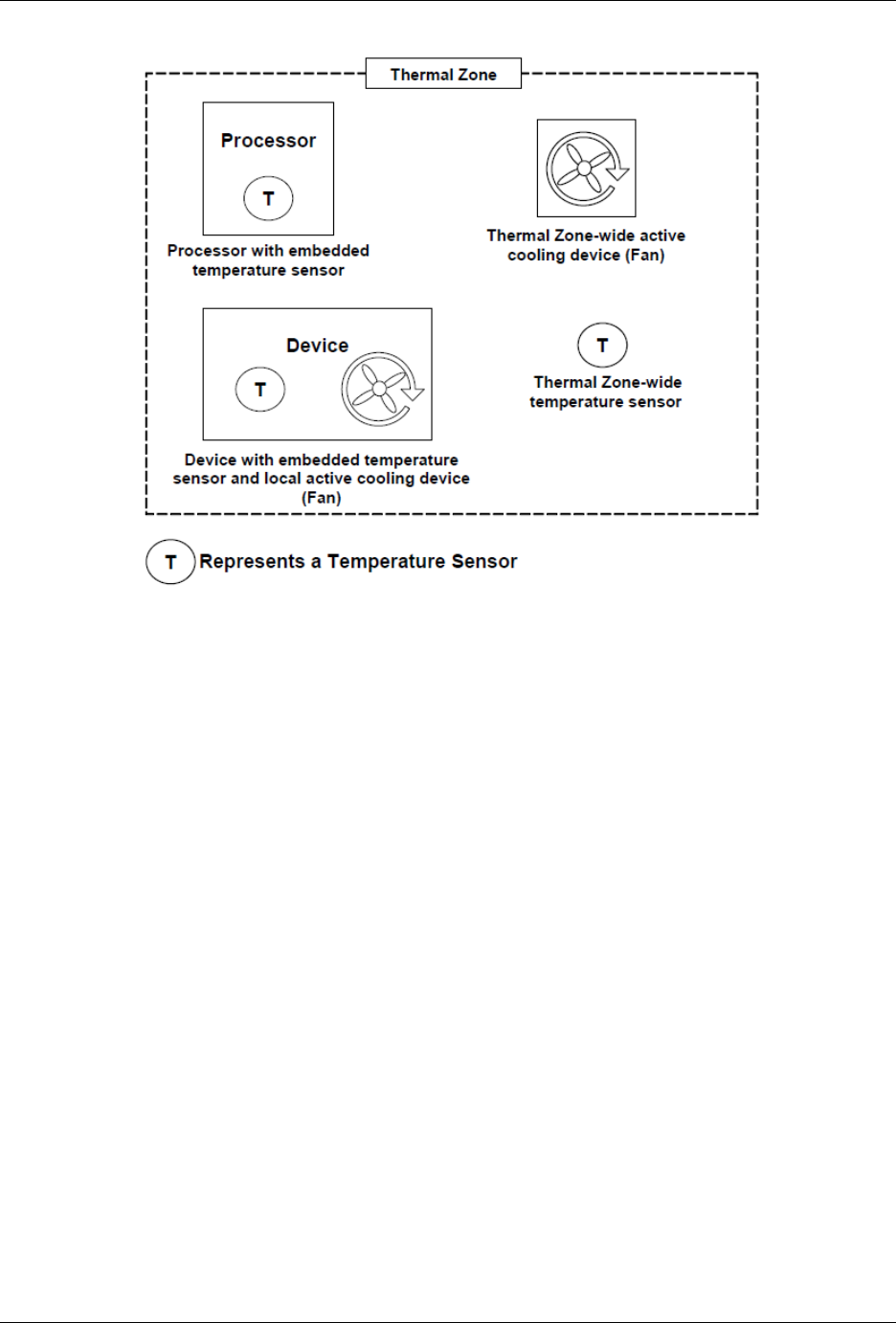
Advanced Configuration and Power Interface (ACPI) Specification, Release 6.5
Fig. 11.1: ACPI Thermal Zone
11.1.1 Active, Passive, and Critical Policies
There are three cooling policies that OSPM uses to control the thermal state of the hardware. The policies are active,
passive and critical.
• Active Cooling. OSPM takes a direct action such as turning on one or more fans. Applying active cooling
controls typically consume power and produce some amount of noise, but are able to cool a thermal zone
without limiting system performance. Active cooling temperature trip points declare the temperature thresholds
OSPM uses to decide when to start or stop different active cooling devices.
• Passive Cooling. OSPM reduces the power consumption of devices to reduce the temperature of a thermal zone,
such as slowing (throttling) the processor clock. Applying passive cooling controls typically produces no user-
noticeable noise. Passive cooling temperature trip points specify the temperature thresholds where OSPM will
start or stop passive cooling.
• Critical Trip Points. These are threshold temperatures at which OSPM performs an orderly, but critical, shut-
down of a device or the entire system. The _HOT object declares the critical temperature at which OSPM may
choose to transition the system into the S4 sleeping state, if supported, The _CRT object declares the critical
temperature at which OSPM must perform a critical shutdown.
When a thermal zone appears in the ACPI Namespace or when a new device becomes a member of a thermal zone,
OSPM retrieves the temperature thresholds (trip points) at which it executes a cooling policy. When OSPM receives a
temperature change notification, it evaluates the thermal zone’s temperature interfaces to retrieve current temperature
values. OSPM compares the current temperature values against the temperature thresholds. If any temperature is
greater than or equal to a corresponding active trip point then OSPM will perform active cooling . If any temperature
is greater than or equal to a corresponding passive trip point then OSPM will perform passive cooling. If the _TMP
object returns a value greater than or equal to the value returned by the _HOT object then OSPM may choose to
transition the system into the S4 sleeping state, if supported. If the _TMP object returns a value greater than or equal
11.1. Thermal Control 664

Advanced Configuration and Power Interface (ACPI) Specification, Release 6.5
to the value returned by the _CRT object then OSPM must shut the system down. Embedded Hot and Critical trip
points may also be exposed by individual devices within a thermal zone. Upon passing of these trip points, OSPM
must decide whether to shut down the device or the entire system based upon device criticality to system operation.
OSPM must also evaluate the thermal zone’s temperature interfaces when any thermal zone appears in the namespace
(for example, during system initialization) and must initiate a cooling policy as warranted independent of receipt of a
temperature change notification. This allows OSPM to cool systems containing a thermal zone whose temperature has
already exceeded temperature thresholds at initialization time.
An optimally designed system that uses several thresholds can notify OSPM of thermal increase or decrease by raising
an event every several degrees. This enables OSPM to anticipate thermal trends and incorporate heuristics to better
manage the system’s temperature.
To implement a preference towards performance or energy conservation, OSPM can request that the platform change
the priority of active cooling (performance) versus passive cooling (energy conservation/silence) by evaluating the
_SCP (Set Cooling Policy) object for the thermal zone or a corresponding OS-specific interface to individual devices
within a thermal zone.
11.1.2 Dynamically Changing Cooling Temperature Trip Points
The platform or its devices can change the active and passive cooling temperature trip points and notify OSPM to
reevaluate the trip point interfaces to establish the new policy threshold settings. The following are the primary uses
for this type of thermal notification:
• When OSPM changes the platform’s cooling policy from one cooling mode to another.
• When a swappable bay device is inserted or removed. A swappable bay is a slot that can accommodate several
different devices that have identical form factors, such as a CD-ROM drive, disk drive, and so on. Many mobile
PCs have this concept already in place.
• After the crossing of an active or passive trip point is signaled to implement hysteresis.
In each situation, OSPM must be notified to re-evaluate the thermal zone’s trip points via the AML code execution
of a Notify(thermal_zone, 0x81) statement or via an OS specific interface invoked by device drivers for zone devices
participating in the thermal model.
11.1.2.1 OSPM Change of Cooling Policy
When OSPM changes the platform’s cooling policy from one cooling mode to the other, the following occurs:
1. OSPM notifies the platform of the new cooling mode by running the Set Cooling Policy (_SCP) control method
in all thermal zones and invoking the OS-specific Set Cooling Policy interface to all participating devices in
each thermal zone.
2. Thresholds are updated in the hardware and OSPM is notified of the change.
3. OSPM re-evaluates the active and passive cooling temperature trip points for the zone and all devices in the zone
to obtain the new temperature thresholds.
11.1. Thermal Control 665

Advanced Configuration and Power Interface (ACPI) Specification, Release 6.5
11.1.2.2 Resetting Cooling Temperatures to Adjust to Bay Device Insertion or Removal
The platform can adjust the thermal zone temperature to accommodate the maximum operating temperature of a bay
device as necessary. For example:
1. Hardware detects that a device was inserted into or removed from the bay, updates the temperature thresholds,
and then notifies OSPM of the thermal policy change and device insertion events.
2. OSPM re-enumerates the devices and re-evaluates the active and passive cooling temperature trip points.
11.1.2.3 Resetting Cooling Temperatures to Implement Hysteresis
An OEM can build hysteresis into platform thermal design by dynamically resetting cooling temperature thresholds.
For example:
1. When the temperature increases to the designated threshold, OSPM will turn on the associated active cooling
device or perform passive cooling.
2. The platform resets the threshold value to a lower temperature (to implement hysteresis) and notifies OSPM of
the change. Because of this new threshold value, the fan will be turned off at a lower temperature than when it
was turned on (therefore implementing a negative hysteresis).
3. When the temperature hits the lower threshold value, OSPM will turn off the associated active cooling device or
cease passive cooling. The hardware will reset _ACx to its original value and notify OSPM that the trip points
have once again been altered.
11.1.3 Detecting Temperature Changes
The ability of the platform and its devices to asynchronously notify an ACPI-compatible OS of meaningful changes
in the thermal zone’s temperature is a highly desirable capability that relieves OSPM from implementing a poll-based
policy and generally results in a much more responsive and optimal thermal policy implementation. Each notification
instructs OSPM to evaluate whether a trip point has been crossed and allows OSPM to anticipate temperature trends
for the thermal zone.
It is recognized that much of the hardware used to implement thermal zone functionality today is not capable of
generating ACPI-visible notifications (SCIs) or only can do so with wide granularity (for example, only when the
temperature crosses the critical threshold). In these environments, OSPM must poll the thermal zone’s temperature
periodically to implement an effective policy.
While ACPI specifies a mechanism that enables OSPM to poll thermal zone temperature, platform reliance on thermal
zone polling is strongly discouraged by this specification. OEMs should design systems that asynchronously notify
OSPM whenever a meaningful change in the zone’s temperature occurs - relieving OSPM of the overhead associ-
ated with polling. In some cases, embedded controller firmware can overcome limitations of existing thermal sensor
capabilities to provide the desired asynchronous notification.
Notice that the _TZP (thermal zone polling) object is used to indicate whether a thermal zone must be polled by
OSPM, and if so, a recommended polling frequency. See _TZP (Thermal Zone Polling) for more information.
11.1. Thermal Control 666

Advanced Configuration and Power Interface (ACPI) Specification, Release 6.5
11.1.3.1 Temperature Change Notifications
Thermal zone-wide temperature sensor hardware that supports asynchronous temperature change notifications does
so using an SCI. The AML code that responds to this SCI must execute a Notify(thermal_zone, 0x80) statement to
inform OSPM that a meaningful change in temperature has occurred. Alternatively, devices with embedded temper-
ature sensors may signal their associated device drivers and the drivers may use an OS-specific interface to signal
OSPM’s thermal policy driver. A device driver may also invoke a device specific control method that executes a
Notify(thermal_zone, 0x80) statement. When OSPM receives this thermal notification, it will evaluate the thermal
zone’s temperature interfaces to evaluate the current temperature values. OSPM will then compare the values to the
corresponding cooling policy trip point values (either zone-wide or device-specific). If the temperature has crossed
over any of the policy thresholds, then OSPM will actively or passively cool (or stop cooling) the system, or shut the
system down entirely.
Both the number and granularity of thermal zone trip points are OEM-specific. However, it is important to notice
that since OSPM can use heuristic knowledge to help cool the system, the more events OSPM receives the better
understanding it will have of the system’s thermal characteristic.
Fig. 11.2: Thermal Events
For example, the simple thermal zone illustrated above includes hardware that will generate a temperature change
notification using a 5° Celsius granularity. All thresholds (_PSV, _AC1, _AC0, and _CRT) exist within the monitored
range and fall on 5 boundaries. This granularity is appropriate for this system as it provides sufficient opportunity
for OSPM to detect when a threshold is crossed as well as to understand the thermal zone’s basic characteristics
(temperature trends).
Note: The ACPI specification defines Kelvin as the standard unit for absolute temperature values. All thermal zone
objects must report temperatures in Kelvin when reporting absolute temperature values. All figures and examples in
this section of the specification use Celsius for reasons of clarity. ACPI allows Kelvin to be declared in precision of
1/10th of a degree (for example, 310.5).
Kelvin is expressed as follows:
𝜃/𝐾 = 𝑇 /(𝑑𝑒𝑔𝑟𝑒𝑒𝑠𝐶𝑒𝑙𝑠𝑖𝑢𝑠) + 273.2
11.1. Thermal Control 667

Advanced Configuration and Power Interface (ACPI) Specification, Release 6.5
11.1.3.2 Polling
Temperature sensor hardware that is incapable of generating thermal change events, or that can do so for only a few
thresholds should inform OSPM to implement a poll-based policy. OSPM does this to ensure that temperature changes
across threshold boundaries are always detectable.
Polling can be done in conjunction with hardware notifications. For example, thermal zone hardware that only supports
a single threshold might be configured to use this threshold as the critical temperature trip point. Assuming that
hardware monitors the temperature at a finer granularity than OSPM would, this environment has the benefit of being
more responsive when the system is overheating.
A thermal zone advertises the need to be polled by OSPM via the _TZP object. See _TZP (Thermal Zone Polling) for
more information.
11.1.4 Active Cooling
Active cooling devices typically consume power and produce some amount of noise when enabled. These devices
attempt to cool a thermal zone through the removal of heat rather than limiting the performance of a device to address
an adverse thermal condition.
The active cooling interfaces in conjunction with the active cooling lists or the active cooling relationship table (_ART)
allow the platform to use an active device that offers varying degrees of cooling capability or multiple cooling devices.
The active cooling temperature trip points designate the temperature where Active cooling is engaged or disengaged
(depending upon the direction in which the temperature is changing). For thermal zone-wide active cooling controls,
the _ALx object evaluates to a list of devices that actively cool the zone or the _ART object evaluates to describe the
entire active cooling relationship of various devices. For example:
• If a standard single-speed fan is the Active cooling device, then _AC0 evaluates to the temperature where active
cooling is engaged and the fan is listed in _AL0.
• If the zone uses two independently controlled single-speed fans to regulate the temperature, then _AC0 will
evaluate to the maximum cooling temperature using two fans, and _AC1 will evaluate to the standard cooling
temperature using one fan.
• If a zone has a single fan with a low speed and a high speed, the _AC0 will evaluate to the temperature associated
with running the fan at high-speed, and _AC1 will evaluate to the temperature associated with running the fan
at low speed. _AL0 and _AL1 will both point to different device objects associated with the same physical fan,
but control the fan at different speeds.
• If the zone uses two independently controlled multiple-speed fans to regulate the temperature, _AC0 of the target
devices evaluates to the temperature at which OSPM will engage fan devices described by the _ART object as
needed up to a maximum capability level.
For ASL coding examples that illustrate these points, see Thermal Zone Interface Requirements and Thermal Zone
Examples.
11.1.5 Passive Cooling
Passive cooling controls are able to cool a thermal zone without creating noise and without consuming additional
power (actually saving power), but do so by decreasing the performance of the devices in the zone .
11.1. Thermal Control 668

Advanced Configuration and Power Interface (ACPI) Specification, Release 6.5
11.1.5.1 Processor Clock Throttling
The processor passive cooling threshold (_PSV) in conjunction with the processor list (_PSL) allows the platform to
indicate the temperature at which a passive control, for example clock throttling, will be applied to the processor(s)
residing in a given thermal zone. Unlike other cooling policies, during passive cooling of processors OSPM may take
the initiative to actively monitor the temperature in order to cool the platform.
On an ACPI-compatible platform that properly implements CPU throttling, the temperature transitions will be similar
to the following figure, in a coolable environment, running a coolable workload:
Fig. 11.3: Temperature and CPU Performance Versus Time
The following equation should be used by OSPM to assess the optimum CPU performance change necessary to lower
the thermal zone’s temperature:
Equation #1
∆𝑃 [%] = _𝑇 𝐶1 * (𝑇
𝑛
− 𝑇
𝑛−1
) + _𝑇 𝐶2 * (𝑇
𝑛
− 𝑇
𝑡
)
Where:
T
n
= current temperature
T
t
= target temperature (_PSV)
The two coefficients _TC1 and _TC2 and the sampling period _TSP are hardware-dependent constants the OEM must
supply to OSPM (for more information, see Section 11.4). The _TSP object contains a time interval that OSPM uses
to poll the hardware to sample the temperature. Whenever the time value returned by _TSP has elapsed, OSPM will
evaluate _TMP to sample the current temperature (shown as T
n
in the above equation). Then OSPM will use the
11.1. Thermal Control 669

Advanced Configuration and Power Interface (ACPI) Specification, Release 6.5
sampled temperature and the passive cooling temperature trip point (_PSV) (which is the target temperature T
t
) to
evaluate the equation for ∆𝑃 . The granularity of ∆𝑃 is determined by the CPU duty width of the system.
Note: Equation #1 has an implied formula.
Equation #2:
𝑃
𝑛
= 𝑃
𝑛−1
+ 𝐻𝑊 [−?𝑃 ]
where:
𝑀𝑖𝑛𝑖𝑚𝑢𝑚% <= 𝑃
𝑛
<= 100%
For this equation, whenever Pn-1 + ?P lies outside the range Minimum0-100%, then Pn will be truncated to
Minimum0-100%. Minimum% is the _MTL limit, or 0% if _MTL is not defined. For hardware that cannot assume all
possible values of Pn between Minimum0 and 100%, a hardware specific mapping function HW is used.
In addition, the hardware mapping function in Equation #2 should be interpreted as follows.
For absolute temperatures:
1. If the right hand side of Equation #1 is negative, 𝐻𝑊 [∆𝑃 ] is rounded to the next available higher setting of
frequency.
2. If the right hand side of Equation #1 is positive, 𝐻𝑊[∆𝑃 ] is rounded to the next available lower setting of
frequency.
For relative temperatures:
1. If the right hand side of Equation #1 is positive, 𝐻𝑊 [∆𝑃 ] is rounded to the next available higher setting of
frequency.
2. If the right hand side of Equation #1 is negative, 𝐻𝑊 [∆𝑃 ] is rounded to the next available lower setting of
frequency.
• The calculated Pn becomes Pn-1 during the next sampling period.
• For more information about CPU throttling, see Processor Power State C0. A detailed explanation of this
thermal feedback equation is beyond the scope of this specification.
11.1.6 Critical Shutdown
When the thermal zone-wide temperature sensor value reaches the threshold indicated by _CRT, OSPM must imme-
diately shut the system down. The system must disable the power either after the temperature reaches some hardware-
determined level above _CRT or after a predetermined time has passed. Before disabling power, platform designers
should incorporate some time that allows OSPM to run its critical shutdown operation. There is no requirement for
a minimum shutdown operation window that commences immediately after the temperature reaches _CRT. This is
because:
• Temperature might rise rapidly in some systems and slowly on others, depending on casing design and environ-
mental factors.
• Shutdown can take several minutes on a server and only a few seconds on a hand-held device.
Because of this indistinct discrepancy and the fact that a critical heat situation is a remarkably rare occurrence, ACPI
does not specify a target window for a safe shutdown. It is entirely up to the OEM to build in a safe buffer that it sees
fit for the target platform.
11.1. Thermal Control 670

Advanced Configuration and Power Interface (ACPI) Specification, Release 6.5
11.2 Cooling Preferences
A robust OSPM implementation provides the means for the end user to convey a preference (or a level of preference)
for either performance or energy conservation to OSPM. Allowing the end user to choose this preference is most
critical to mobile system users where maximizing system run-time on a battery charge often has higher priority over
realizing maximum system performance. For example, if a user is taking notes on her PC in a quiet environment, such
as a library or a corporate meeting, she may want the system to emphasize passive cooling so that the system operates
quietly, even at the cost of system performance.
A user preference towards performance corresponds to the Active cooling mode while a user’s preference towards
energy conservation or quiet corresponds to the Passive cooling mode. ACPI defines an interface to convey the cooling
mode to the platform. Active cooling can be performed with minimal OSPM thermal policy intervention. For example,
the platform indicates through thermal zone parameters that crossing a thermal trip point requires a fan to be turned
on. Passive cooling requires OSPM thermal policy to manipulate device interfaces that reduce performance to reduce
thermal zone temperature.
Either cooling mode will be activated only when the thermal condition requires it. When the thermal zone is at
an optimal temperature level where it does not warrant any cooling, both modes result in a system operating at its
maximum potential with all fans turned off.
Thermal zones supporting the Set Cooling Policy interface allow the user to switch the system’s cooling mode empha-
sis. See _SCP (Set Cooling Policy) for more information.
Fig. 11.4: Active and Passive Threshold Values
As illustrated in Active and Passive Threshold Values, the platform must convey the value for each threshold to instruct
OSPM to initiate the cooling policies at the desired target temperatures. The platform can emphasize active or passive
cooling modes by assigning different threshold values. Generally, if _ACx is set lower than _PSV, then the system
emphasizes active cooling. Conversely, if _PSV is set lower than _ACx, then the emphasis is placed on passive cooling.
For example, a thermal zone that includes a processor and one single-speed fan may use _PSV to indicate the tempera-
ture value at which OSPM would enable passive cooling and _AC0 to indicate the temperature at which the fan would
be turned on. If the value of _PSV is less than _AC0 then the system will favor passive cooling (for example, CPU
clock throttling). On the other hand, if _AC0 is less than _PSV the system will favor active cooling (in other words,
using the fan). See the figure below for more details.
11.2. Cooling Preferences 671

Advanced Configuration and Power Interface (ACPI) Specification, Release 6.5
Fig. 11.5: Cooling Preferences
The example on the left enables active cooling (for example, turn on a fan) when OSPM detects the temperature has
risen above 50°. If for some reason the fan does not reduce the system temperature, then at 75° OSPM will initiate
passive cooling (for example, CPU throttling) while still running the fan. If the temperature continues to climb, OSPM
will quickly shut the system down when the temperature reaches 90°C. The example on the right is similar but the
_AC0 and _PSV threshold values have been swapped to emphasize passive cooling.
The ACPI thermal model allows flexibility in the thermal zone design. An OEM that needs a less elaborate thermal
implementation may consider using only a single threshold (for example, _CRT). Complex thermal implementations
can be modeled using multiple active cooling thresholds and devices, or through the use of additional thermal zones.
11.2.1 Evaluating Thermal Device Lists
The Notify(thermal_zone, 0x82) statement is used to inform OSPM that a change has been made to the thermal zone
device lists. This thermal event instructs OSPM to re-evaluate the _ALx, _PSL, and _TZD objects.
For example, a system that supports the dynamic insertions of processors might issue this notification to inform OSPM
of changes to _PSL following the insertion or removal of a processor. OSPM would re-evaluate all thermal device lists
and adjust its policy accordingly.
Notice that this notification can be used with the Notify(thermal_zone, 0x81) statement to inform OSPM to both
re-evaluate all device lists and all thresholds.
Alternatively, devices may include the _TZM (Thermal Zone Member) object their device scope to convey their
thermal zone association to OSPM. See _TZM (Thermal Zone Member) below for more information.
11.2.2 Evaluating Device Thermal Relationship Information
The Notify(thermal_zone, 0x83) statement is used to inform OSPM that a change has been made to the thermal
relationship information. This thermal event instructs OSPM to re-evaluate the _TRT and _ART objects. The thermal
influence between devices may change when active cooling moves air across device packages as compared to when
only passive cooling controls are applied. Similarly, the active cooling relationship may change as various fans are
engaged to actively cool a platform or if user preferences change.
11.2. Cooling Preferences 672

Advanced Configuration and Power Interface (ACPI) Specification, Release 6.5
11.2.3 Fan Device Notifications
Notify events of type 0x80 will cause OSPM to evaluate the _FST object to evaluate the fan’s current speed.
11.3 Fan Device
ACPI 1.0 defined a simple fan device that is assumed to be in operation when it is in the D0 state. Thermal zones
reference fan device(s) as being responsible primarily for cooling within that zone. Notice that multiple fan devices
can be present for any one thermal zone. They might be actual different fans, or they might be used to implement one
fan of multiple speeds (for example, by turning both “fans” on the one fan will run full speed).
ACPI 4.0 defines additional fan device interface objects enabling OSPM to perform more robust active cooling thermal
control. These objects are summarized (see Table 11.1 below). OSPM requires that all of the objects listed in the table
below be defined under a fan device to enable advanced active cooling control. The absence of any of these objects
causes OSPM to perform ACPI 1.0 style simple fan control .
The Plug and Play ID of a fan device is PNP0C0B.
Table 11.1: Fan Specific Objects
Object Description
_FIF Returns fan device information.
_FPS Returns a list of supported fan performance states.
_FSL Control method that sets the fan device’s speed level (performance state).
_FST Returns current status information for a fan device.
While the Fan Device and its associated objects are optional, if the Fan Device is implemented by the platform, all
objects listed in the table above are required and must be provided.
11.3.1 Fan Objects
11.3.1.1 _FIF (Fan Information)
The optional _FIF object provides OSPM with fan device capability information.
Arguments:
None
Return Value:
A Package containing the fan device parameters as described in the table below
_FIF evaluation returns a package of the following format:
Package (){
Revision, // Integer
FineGrainControl, // Integer Boolean
StepSize // Integer DWORD
LowSpeedNotificationSupport // Integer Boolean
}
11.3. Fan Device 673

Advanced Configuration and Power Interface (ACPI) Specification, Release 6.5
Table 11.2: FIF Package Details
Field Format Description
Revision Integer Current revision is: 0
Fine Grain
Control
Integer
(Boolean)
A non zero value in this field indicates OSPM may evaluate the fan device’s
_FSL object with a Level argument value in the range of 0-100, which repre-
sents a percentage of maximum speed. A zero value in this field indicates that
OSPM may evaluate the fan device’s _FSL object with a Level argument value
that is a Control field value from a package in the _FPS object’s package list
only.
Step Size Integer
(DWORD)
The recommended minimum step size in percentage points to be used when
OSPM performs fine-grained fan speed control. OSPM may utilize the value
of this field if the FineGrainControl field is non-zero the value in this field is
between 1 and 9.
Low Speed
Notification
Support
Integer
(Boolean)
A non zero value in this field indicates that the platform will issue a Notify
(0x80) to the fan device if a low (errant) fan speed is detected.
If a fan device supports fine-grained control, OSPM may evaluate a fan device’s _FSL object with any Level argument
value that is less than or equal to the Control field value specified in the package of the _FPS object’s package list
that corresponds to the active cooling trip point that has been exceeded. This capability provides OSPM access to one
hundred fan speed settings thus enabling fine-grained fan speed control. The platform uses the StepSize field to help
OSPM optimize its fan level selection policy by fine-grained fan speed control. The platform uses the StepSize field
to help OSPM optimize its fan level selection policy by indicating recommended increments in the fan speed level
value that are appropriate for the fan when one percent increments are not optimal. In the event OSPM’s incremental
selections of Level using the StepSize field value do not sum to 100%, OSPM may select an appropriate ending Level
increment to reach 100%. OSPM should use the same residual step value first when reducing Level.
11.3.1.2 _FPS (Fan Performance States)
The optional _FPS object evaluates to a variable-length package containing a list of packages that describe the fan
device’s performance states. A temperature reading above an active cooling trip point defined by an _ACx object in
a thermal zone or above a native active cooling trip point of a device within the thermal zone causes OSPM thermal
control to engage the appropriate corresponding fan performance state from the list of fan performance states described
by the _FPS object if the fan device is present in the corresponding _ALx device list or if an entry exists for the fan
and trip point in the active cooling relationship table (_ART).
OSPM assumes a linear relationship for the acoustic impact and power consumption values between successive entries
in the fan performance state list. Notice that the acoustic impact measurement unit (Decibels) is inherently non-linear.
As such, the platform should populate _FPS entries as necessary to enable OSPM to achieve optimal results.
Arguments:
None
Return Value:
A variable-length Package containing a Revision ID and a list of Packages that describe the fan device’s
performance states as described in the table below.
Return Value Information
Package {
Revision, // Integer - Current revision is: 0
FanPState[0], // Package
....
(continues on next page)
11.3. Fan Device 674

Advanced Configuration and Power Interface (ACPI) Specification, Release 6.5
(continued from previous page)
FanPState[n] // Package
}
Each FanPState sub-Package contains the elements described below:
Package () // Fan P-State
{
Control, // Integer DWORD
TripPoint, // Integer DWORD
Speed, // Integer DWORD
NoiseLevel, // Integer DWORD
Power // Integer DWORD
}
Table 11.3: FPS FanPstate Package Details
Field Format Description
Control Integer (DWORD) Indicates the value to be used to set the fan speed to a specific level
using the _FSL object. If the fan device supports fine-grained con-
trol as indicated by the _FIF object, this value is a percentage (0-
100) of maximum speed level. If the fan device does not support
fine-grained control, this field is an opaque value that OSPM must
simply use in its evaluation of the _FSL object to set the level to this
performance state.
TripPoint Integer (DWORD) 0-9: The active cooling trip point number that corresponds to this
performance state. If the _ART object is defined, OSPM may op-
tionally use information provided by the _ART object and _FPS
objects to select alternative fan performance states. Only one en-
try per unique trip point number is allowed in the _FPS. 0x0A-
0xFFFFFFFE: Reserved 0x0FFFFFFFF: Indicates that this perfor-
mance state does not correspond with a specific active cooling trip
point.
Speed Integer (DWORD) Indicates the speed of the fan in revolutions per minute in this per-
formance state.
NoiseLevel Integer (DWORD) This optional field indicates the audible noise emitted by the fan
in this performance state. The value represents the noise in 10ths
of decibels. For example, if the fan emits noise at 28.3dB in this
performance state, the value of this field would be 283. A value of
0xFFFFFFFF indicates that this field is not populated.
Power Integer (DWORD) This optional field indicates the power consumption (in milliwatts)
of the fan in this performance state. For example, if the fan con-
sumes .5W in this performance state, the value of this field would
be 500. A value of 0xFFFFFFFF indicates that this field is not pop-
ulated.
11.3. Fan Device 675

Advanced Configuration and Power Interface (ACPI) Specification, Release 6.5
11.3.1.3 _FSL (Fan Set Level)
The optional _FSL object is a control method that OSPM evaluates to set a fan device’s speed (performance state) to
a specific level
Arguments:(1)
Arg0 - Level (Integer): conveys to the platform the fan speed level to be set.
Return Value:
None
Argument Information
Arg0: Level. If the fan supports fine-grained control, Level is a percentage of maximum level (0-100) that
the platform is to engage the fan. If the fan does not support fine-grained control, Level is a Control field
value from a package in the _FPS object’s package list. A Level value of zero causes the platform to turn
off the fan.
11.3.1.4 _FST (Fan Status)
The optional _FST object provides status information for the fan device.
Arguments:
None
Return Value:
A Package containing fan device status information as described in the table below
_FST evaluation returns a package of the following format:
Package (){
Revision, // Integer
Control, // Integer DWORD
Speed // Integer DWORD
}
Table 11.4: FST Package Details
Field Format Description
Revision Integer Current revision is: 0
Control Integer (DWORD) The current control value used to operate the Fan. If the fan is not
operating Control will be zero. If the fan is operating, Control is the
Level argument passed in the evaluation of the _FSL object.
Speed Integer (DWORD) The current fan speed in revolutions per minute at which the fan is
rotating. A value of 0xFFFFFFFF indicates that the fan does not
support speed reporting.
11.3. Fan Device 676

Advanced Configuration and Power Interface (ACPI) Specification, Release 6.5
11.4 Thermal Objects
Objects related to thermal management are listed in the following table.
Table 11.5: Thermal Objects
Object Description
_ACx Returns active cooling policy threshold values in tenths of degrees.
_ALx List of active cooling device objects.
_ART Table of values that convey the Active Cooling Relationship between devices
_CRT Returns critical trip point in tenths of degrees where OSPM must perform a critical shutdown.
_HOT Returns critical trip point in tenths of degrees where OSPM may choose to transition the system
into S4.
_MTL Returns the minimum throttle limit of a zone, when defined under a thermal zone. T
_NTT Returns the temperature change threshold for devices containing native temperature sensors to
cause evaluation of the _TPT object
_PSL List of processor device objects for clock throttling.
_PSV Returns the passive cooling policy threshold value in tenths of degrees.
_RTV Conveys whether temperatures are expressed in terms of absolute or relative values.
_SCP Sets platform cooling policy (active or passive).
_STR String name for this thermal zone.
_TC1 Thermal constant for passive cooling.
_TC2 Thermal constant for passive cooling.
_TFP Thermal fast sampling period for Passive cooling in milliseconds.
_TMP Returns the thermal zone’s current temperature in tenths of degrees.
_TPT Conveys the temperature of a devices internal temperature sensor to the platform when a temper-
ature trip point is crossed or a meaningful change in temperature occurs.
_TRT Table of values that convey the Thermal Relationship between devices
_TSN Returns a reference to the thermal sensor device used to monitor the temperature of the thermal
zone (when defined under a thermal zone).
_TSP Thermal sampling period for Passive cooling in tenths of seconds.
_TST Conveys the minimum separation for a devices’ programmable temperature trip points.
_TZD List of devices whose temperature is measured by this thermal zone.
_TZM Returns the thermal zone for which a device is a member.
_TZP Thermal zone polling frequency in tenths of seconds.
With the exception of _TPT, _TST, and the _TZM objects, the objects described in the following sections may exist
under a thermal zone. Devices with embedded thermal sensors and controls may contain static cooling temperature
trip points or dynamic cooling temperature trip points that must be programmed by the device’s driver. In this case,
thermal objects defined under a device serve to convey the platform specific values for these settings to the devices
driver.
11.4.1 _ACx (Active Cooling)
This optional object, if present under a thermal zone, returns the temperature trip point at which OSPM must start or
stop Active cooling, where x is a value between 0 and 9 that designates multiple active cooling levels of the thermal
zone. If the Active cooling device has one cooling level (that is, “on”) then that cooling level must be defined as _AC0.
If the cooling device has two levels of capability, such as a high fan speed and a low fan speed, then they must be
defined as _AC0 and _AC1 respectively. The smaller the value of x, the greater the cooling strength _ACx represents.
In the above example, _AC0 represents the greater level of cooling (the faster fan speed) and _AC1 represents the
lesser level of cooling (the slower fan speed). For every _ACx method, there must be a matching _ALx object or a
corresponding entry in an _ART object’s active cooling relationship list.
11.4. Thermal Objects 677

Advanced Configuration and Power Interface (ACPI) Specification, Release 6.5
If this object it present under a device, the device’s driver evaluates this object to determine the device’s corresponding
active cooling temperature trip point. This value may then be used by the device’s driver to program an internal device
temperature sensor trip point. When this object is present under a device, the device must contain a native OS device
driver interface supporting a corresponding active cooling control, a matching _ALx object under the thermal zone of
which the device is a member must exist, or a corresponding entry in an _ART object’s active cooling relationship list
must.
Arguments:
None
Return Value:
An Integer containing the active cooling temperature threshold in tenths of degrees Kelvin
The return value is an integer that represents tenths of degrees Kelvin. For example, 300.0K is represented by the
integer 3000.
11.4.2 _ALx (Active List)
This object is defined under a thermal zone and evaluates to a list of Active cooling devices to be turned on when the
corresponding _ACx temperature threshold is exceeded. For example, these devices could be fans.
Arguments:
None
Return Value:
A variable-length Package containing a list of References to active cooling devices
The return value is a package consisting of references to all active cooling devices that should be engaged when the
associated active cooling threshold (_ACx) is exceeded.
When the returned package consists of references to an active cooling device that is a fan device and the fan device
implements _FPS and _FSL objects, OSPM activates the identified fan at a capability level matching the level identified
by this object. For example, if the system has a fan that implements _FPS object with 5 levels, and if _AL3 is evaluated
by the OSPM causing it to return this fan’s reference, then the fan is activated by evaluating _FSL with the value from
the Control field of an _FPS entry whose TripPoint field value equals 3.
If a thermal zone has the _ART object defined, then it is not necessary to have any _ALx objects implemented.
Note: If a thermal zone has _ART object defined as well as _ALx defined, the OSPM ignores _ALx objects and uses
_ART exclusively.
11.4.3 _ART (Active Cooling Relationship Table)
The optional _ART object evaluates to a variable-length package containing a list of packages each of which describes
the active cooling relationship between a device within a thermal zone and an active cooling device. OSPM uses the
combined information about the active cooling relationships of all devices in the thermal zone to make active cooling
policy decisions.
If _ART is implemented within a thermal zone, OSPM ignores all _ALx objects as _ART conveys a mapping for each
of the _ACx trip points to active cooling devices.
The platform can dynamically change the _ART object by notifying the thermal zone object with a Notify code of
0x83, which will cause OSPM to re-evaluate both the _TRT and _ART objects. This allows the platform to change the
capability level mapping to various _ACx trip points dynamically at run time.
11.4. Thermal Objects 678

Advanced Configuration and Power Interface (ACPI) Specification, Release 6.5
Arguments:
None
Return Value:
A variable-length Package containing a Revision ID and a list of Active Relationship Packages as de-
scribed below:
Return Value Information
Package {
Revision, // Integer - Current revision is: 0
ActiveRelationship[0] // Package
....
ActiveRelationship[n] // Package
}
Each ActiveRelationship sub-Package contains the elements described below:
Package {
SourceDevice, // Object Reference to a Fan Device Object
TargetDevice, // Object Reference to a Device Object
Weight, // Integer
AC0MaxLevel, // Integer
AC1MaxLevel, // Integer
AC2MaxLevel, // Integer
AC3MaxLevel, // Integer
AC4MaxLevel, // Integer
AC5MaxLevel, // Integer
AC6MaxLevel, // Integer
AC7MaxLevel, // Integer
AC8MaxLevel, // Integer
AC9MaxLevel // Integer
}
Table 11.6: Thermal Relationship Package Values 1
Element Object Type Description
SourceDevice Reference (to a de-
vice)
The fan device that has an impact on the cooling of the device indi-
cated by TargetDevice.
TargetDevice Reference (to a de-
vice)
The device that is impacted by the fan device indicated by
SourceDevice.
Weight Integer Indicates the SourceDevice’s contribution to the platform’s Target-
Device total cooling capability when the fans of all entries in the
_ART with the same target device are engaged at their highest (max-
imum capability) performance state. This is represented as a per-
centage value (0-100).
AC0MaxLevel Integer (DWORD) Indicates the maximum fans speed level in percent (0-100) that
OSPM may engage on the SourceDevice when a temperature ex-
ceeds the _AC0 trip point value. A value of 0xFFFFFFFF in this
field indicates that the SourceDevice is not to be engaged for the
trip point.
continues on next page
11.4. Thermal Objects 679

Advanced Configuration and Power Interface (ACPI) Specification, Release 6.5
Table 11.6 – continued from previous page
Element Object Type Description
AC1MaxLevel Integer (DWORD) Indicates the maximum fans speed level in percent (0-100) that
OSPM may engage on the SourceDevice when a temperature ex-
ceeds the _AC1 trip point value. A value of 0xFFFFFFFF in this
field indicates that the SourceDevice is not to be engaged for the
trip point.
AC2MaxLevel Integer (DWORD) Indicates the maximum fans speed level in percent (0-100) that
OSPM may engage on the SourceDevice when a temperature ex-
ceeds the _AC2 trip point value. A value of 0xFFFFFFFF in this
field indicates that the SourceDevice is not to be engaged for the
trip point.
AC3MaxLevel Integer (DWORD) Indicates the maximum fans speed level in percent (0-100) that
OSPM may engage on the SourceDevice when a temperature ex-
ceeds the _AC3 trip point value. A value of 0xFFFFFFFF in this
field indicates that the SourceDevice is not to be engaged for the
trip point.
AC4MaxLevel Integer (DWORD) Indicates the maximum fans speed level in percent (0-100) that
OSPM may engage on the SourceDevice when a temperature ex-
ceeds the _AC4 trip point value. A value of 0xFFFFFFFF in this
field indicates that the SourceDevice is not to be engaged for the
trip point.
AC5MaxLevel Integer (DWORD) Indicates the maximum fans speed level in percent (0-100) that
OSPM may engage on the SourceDevice when a temperature ex-
ceeds the _AC5 trip point value. A value of 0xFFFFFFFF in this
field indicates that the SourceDevice is not to be engaged for the
trip point.
AC6MaxLevel Integer (DWORD) Indicates the maximum fans speed level in percent (0-100) that
OSPM may engage on the SourceDevice when a temperature ex-
ceeds the _AC6 trip point value. A value of 0xFFFFFFFF in this
field indicates that the SourceDevice is not to be engaged for the
trip point.
AC7MaxLevel Integer (DWORD) Indicates the maximum fans speed level in percent (0-100) that
OSPM may engage on the SourceDevice when a temperature ex-
ceeds the _AC7 trip point value. A value of 0xFFFFFFFF in this
field indicates that the SourceDevice is not to be engaged for the
trip point.
AC8MaxLevel Integer (DWORD) Indicates the maximum fans speed level in percent (0-100) that
OSPM may engage on the SourceDevice when a temperature ex-
ceeds the _AC8 trip point value. A value of 0xFFFFFFFF in this
field indicates that the SourceDevice is not to be engaged for the
trip point.
AC9MaxLevel Integer (DWORD) Indicates the maximum fans speed level in percent (0-100) that
OSPM may engage on the SourceDevice when a temperature ex-
ceeds the _AC9 trip point value. A value of 0xFFFFFFFF in this
field indicates that the SourceDevice is not to be engaged for the
trip point.
In the case multiple active cooling trip points have been exceeded and _ART entries indicate various maximum limits
for the same SourceDevice, OSPM may operate the SourceDevice up to the highest ACxMaxLevel value indicated for
all exceeded trip points.
11.4. Thermal Objects 680

Advanced Configuration and Power Interface (ACPI) Specification, Release 6.5
11.4.4 _CRT (Critical Temperature)
This object, when defined under a thermal zone, returns the critical temperature at which OSPM must shutdown the
system. If this object it present under a device, the device’s driver evaluates this object to determine the device’s
critical cooling temperature trip point. This value may then be used by the device’s driver to program an internal
device temperature sensor trip point.
Arguments:
None
Return Value:
An Integer containing the critical temperature threshold in tenths of degrees Kelvin
The result is an integer value that represents the critical shutdown threshold in tenths of degrees. For example, 300.0K
is represented by the integer 3000.
11.4.5 _CR3 (Warm/Standby Temperature)
This object, when defined under a thermal zone, returns the critical temperature at which OSPM may choose to
transition the system into a low power state with a faster exit latency than S4 sleeping state (e.g. S3, or an equivalent
low power state if the LOW_POWER_S0_IDLE_CAPABLE FADT flag is set). The platform vendor should define
_CR3 to be sufficiently below _CRT so as to allow enough time to transition the system into this low power state.
It may be sufficient to define either _CR3 or _HOT depending on the type and thermal characteristics of the specific
thermal zone under consideration. If this object it present under a device, the device’s driver evaluates this object to
determine the device’s warm/standby cooling temperature trip point. This value may then be used by the device’s
driver to program an internal device temperature sensor trip point.
Arguments:
None
Return Value:
An Integer containing the critical temperature threshold in tenths of degrees Kelvin
The result is an integer value that represents the critical shutdown threshold in tenths of degrees. For example, 300.0K
is represented by the integer 3000.
11.4.6 _DTI (Device Temperature Indication)
This optional object may be present under a device and is evaluated by OSPM when the device’s native (driver man-
aged) temperature sensor has crossed a cooling temperature trip point or when a meaningful change in temperature (as
indicated by evaluation of the _NTT object) has occurred. OSPM evaluation of the _DTI object enables the platform
to take action as a result of these events. For example, the platform may choose to implement fan control hysteresis
based on the conveyed value or signal the revaluation of the _TDL or _PDL objects.
Arguments:(1)
Arg0 - An Integer containing the current value of the temperature sensor (in tenths Kelvin)
Return Value:
None
11.4. Thermal Objects 681

Advanced Configuration and Power Interface (ACPI) Specification, Release 6.5
11.4.7 _HOT (Hot Temperature)
This optional object, when defined under a thermal zone, returns the critical temperature at which OSPM may choose
to transition the system into the S4 sleeping state. The platform vendor should define _HOT to be far enough below
_CRT so as to allow OSPM enough time to transition the system into the S4 sleeping state. While dependent on
the amount of installed memory, on typical platforms OSPM implementations can transition the system into the S4
sleeping state in tens of seconds. If this object it present under a device, the device’s driver evaluates this object
to determine the device’s hot cooling temperature trip point. This value may then be used by the device’s driver to
program an internal device temperature sensor trip point.
Arguments:
None
Return Value:
An Integer containing the critical temperature threshold in tenths of degrees Kelvin
The return value is an integer that represents the critical sleep threshold tenths of degrees Kelvin. For example, 300.0K
is represented by the integer 3000.
11.4.8 _MTL (Minimum Throttle Limit)
This object, when defined under a thermal zone, returns the minimum throttle limit of a zone. This will determine how
much a thermal zone limits the performance of its controlled devices. This value can be used by OSPM to calculate
the changes in performance limits it applies to the devices of the thermal zone.
Arguments:
None
Return Value:
An Integer value with the current minimum throttle limit, expressed as a percentage
11.4.9 _NTT (Notification Temperature Threshold)
This optional object may be defined under devices containing native temperature sensors and evaluates to the tempera-
ture change threshold for the device where the platform requires notification of the change via evaluation of the _TPT
object.
Arguments:
None
Return Value:
An Integer containing the temperature threshold in tenths of degrees Kelvin.
The return value is an integer that represents the amount of change in device temperature that is meaningful to the
platform and for which the platform requires notification via evaluation of the _TPT object.
11.4. Thermal Objects 682

Advanced Configuration and Power Interface (ACPI) Specification, Release 6.5
11.4.10 _PSL (Passive List)
This object is defined under a thermal zone and evaluates to a list of processor objects to be used for passive cooling.
Arguments:
None
Return Value:
A variable-length Package containing a list of References to processor objects
The return value is a package consisting of references to all processor objects that will be used for passive cooling
when the zone’s passive cooling threshold (_PSV) is exceeded.
11.4.11 _PSV (Passive)
This optional object, if present under a thermal zone, evaluates to the temperature at which OSPM must activate
passive cooling policy.
Arguments:
None
Return Value:
An Integer containing the passive cooling temperature threshold in tenths of degrees Kelvin
The return value is an integer that represents tenths of degrees Kelvin. For example, 300.0 Kelvin is represented by
3000.
If this object it present under a device, the device’s driver evaluates this object to determine the device’s corresponding
passive cooling temperature trip point. This value may then be used by the device’s driver to program an internal
device temperature sensor trip point. When this object is present under a device, the device must contain a native OS
device driver interface supporting a passive cooling control.
11.4.12 _RTV (Relative Temperature Values)
This optional object may be present under a device or a thermal zone and is evaluated by OSPM to determine whether
the values returned by temperature trip point and current operating temperature interfaces under the corresponding
device or thermal zone represent absolute or relative temperature values.
Arguments:
None
Return Value:
An Integer containing a relative versus absolute indicator:
0 Temperatures are absolute Other Temperatures are relative
The return value is an integer that indicates whether values returned by temperature trip point and current operating
temperature interfaces represent absolute or relative temperature values.
If the _RTV object is not present or is present and evaluates to zero then OSPM assumes that all values returned by
temperature trip point and current operating temperature interfaces under the device or thermal zone represent absolute
temperature values expressed in tenths of degrees Kelvin.
If the _RTV object is present and evaluates to a non zero value then all values returned by temperature trip point
and current operating temperature interfaces under the corresponding device or thermal zone represent temperature
values relative to a zero point that is defined as the maximum value of the device’s or thermal zone’s critical cooling
11.4. Thermal Objects 683

Advanced Configuration and Power Interface (ACPI) Specification, Release 6.5
temperature trip point. In this case, temperature trip point and current operating temperature interfaces return values
in units that are tenths of degrees below the zero point.
OSPM evaluates the _RTV object before evaluating any other temperature trip point or current operating temperature
interfaces.
11.4.13 _SCP (Set Cooling Policy)
This optional object is a control method that OSPM invokes to set the platform’s cooling mode policy setting. The
platform may use the evaluation of _SCP to reassign _ACx and _PSV temperature trip points according to the mode
or limits conveyed by OSPM. OSPM will automatically evaluate _ACx and _PSV objects after executing _SCP. This
object may exist under a thermal zone or a device.
Arguments:(3)
Arg0 - Mode An Integer containing the cooling mode policy code
Arg1 - AcousticLimit An Integer containing the acoustic limit
Arg2 - PowerLimit An Integer containing the power limit
Return Value:
None
Argument Information:
Mode - 0 = Active, 1 = Passive
Acoustic Limit - Specifies the maximum acceptable acoustic level that active cooling devices may generate. Values are
1 to 5 where 1 means no acoustic tolerance and 5 means maximum acoustic tolerance.
Power Limit - Specifies the maximum acceptable power level that active cooling devices may consume. Values are
from 1 to 5 where 1 means no power may be used to cool and 5 means maximum power may be used to cool.
Example:
// Fan Control is defined as follows:
// Speed 1 (Fan is Off): Acoustic Limit 1, Power Limit 1, <= 64C
// Speed 2: Acoustic Limit 2, Power Limit 2, 65C - 74C
// Speed 3: Acoustic Limit 3, Power Limit 3, 75C - 84C
// Speed 4: Acoustic Limit 4, Power Limit 4, 85C - 94C
// Speed 5: Acoustic Limit 5, Power Limit 5, >= 95C
// _SCP Notifies the platform the current cooling mode.
// Arg0 = Mode
// 0 - Active cooling
// 1 - Passive cooling
// Arg1 = Acoustic Limit
// 1 = No acoustic tolerance
// ...
// 5 = maximum acoustic tolerance
// Arg2 = Power Limit
// 1 = No power may be used to cool
// ...
// 5 = maximum power may be used to cool
Method(_SCP,3,Serialized)
{
(continues on next page)
11.4. Thermal Objects 684

Advanced Configuration and Power Interface (ACPI) Specification, Release 6.5
(continued from previous page)
// Store the Cooling Mode in NVS and use as needed in
// the rest of the ASL Code.
Store(Arg0, CTYP)
// Set PSVT to account for a Legacy OS that does not pass
// in either the acoustic limit or Power Limit.
If(Arg0)
{
Store(60,PSVT)
}
Else
{
Store(97,PSVT)
}
If (CondRefOf (_OSI,Local0))
{
If (\_OSI ("3.0 _SCP Extensions"))
{
// Determine Power Limit.
//
// NOTE1: PSVT = Passive Cooling Trip Point stored
// in NVS in Celsius.
//
// NOTE2: 4 Active Cooling Trips Points correspond to 5
// unique Power Limit regions and 5 unique acoustic limit
// regions.
//
// NOTE3: This code will define Passive cooling so that
// CPU throttling will be initiated within the Power Limit
// Region passed in such that the next higher Power Limit
// Region will not be reached.
Switch(Arg2)
{
Case(1) // Power Limit = 1.
{
// Stay in Acoustic Limit 1.
Store(60,PSVT) // Passive = 60C.
}
Case(2) // Power Limit = 2.
{
// Store Highest supported Acoustic Level
// at this Power Limit (1 or 2).
Store(70,PSVT)
If(Lequal(Arg1,1))
{
// Stay in Acoustic Level 1.
Store(60,PSVT)
}
}
Case(3) // Power Limit = 3.
{
// Store Highest supported Acoustic Level
// at this Power Limit (1, 2, or 3).
Store(80,PSVT)
If(Lequal(Arg1,2))
(continues on next page)
11.4. Thermal Objects 685

Advanced Configuration and Power Interface (ACPI) Specification, Release 6.5
(continued from previous page)
{
// Stay in Acoustic Level 1 or 2.
Store(70,PSVT)
}
If(Lequal(Arg1,1))
{
// Stay in Acoustic Level 1.
Store(60,PSVT)
}
}
Case(4) // Power Limit = 4.
{
// Store Highest supported Acoustic Level
// at this Power Limit (1, 2, 3, or 4).
Store(90,PSVT)
If(Lequal(Arg1,3))
{
// Stay in Acoustic Level 1 or 2.
Store(80,PSVT)
}
If(Lequal(Arg1,2))
{
// Stay in Acoustic Level 1 or 2.
Store(70,PSVT)
}
If(Lequal(Arg1,1))
{
// Stay in Acoustic Level 1.
Store(60,PSVT)
}
}
Case(5) // Power Limit = 5.
{
// Store Highest supported Acoustic Level
// at this Power Limit (1, 2, 3, 4, or 5).
Store(97,PSVT)
If(Lequal(Arg1,4))
{
// Stay in Acoustic Level 1 or 2.
Store(90,PSVT)
}
If(Lequal(Arg1,3))
{
// Stay in Acoustic Level 1 or 2.
Store(80,PSVT)
}
If(Lequal(Arg1,2))
{
// Stay in Acoustic Level 1 or 2.
Store(70,PSVT)
}
If(Lequal(Arg1,1))
{
// Stay in Acoustic Level 1.
Store(60,PSVT)
}
} // Case 5
(continues on next page)
11.4. Thermal Objects 686

Advanced Configuration and Power Interface (ACPI) Specification, Release 6.5
(continued from previous page)
} // Switch Arg 2
} // \_OSI - Extended \_SCP
} // CondRefOf \_OSI
} // Method \_SCP
11.4.14 _STR (String)
This optional object, when defined under a thermal zone, returns a string name for this thermal zone. See below for
more details.
11.4.15 _TC1 (Thermal Constant 1)
This object evaluates to the constant _TC1 for use in the Passive cooling formula:
∆𝑃 𝑒𝑟𝑓𝑜𝑟𝑚𝑎𝑛𝑐𝑒[%] = _𝑇 𝐶1 * (𝑇
𝑛
− 𝑇
𝑛−1
) + _𝑇 𝐶2 * (𝑇
𝑛
− 𝑇
𝑡
)
Arguments:
None
Return Value:
An Integer containing Thermal Constant #1
11.4.16 _TC2 (Thermal Constant 2)
This object evaluates to the constant _TC2 for use in the Passive cooling formula:
∆𝑃 𝑒𝑟𝑓𝑜𝑟𝑚𝑎𝑛𝑐𝑒[%] = _𝑇 𝐶1 * (𝑇
𝑛
− 𝑇
𝑛−1
) + _𝑇 𝐶2 * (𝑇
𝑛
− 𝑇
𝑡
)
Arguments:
None
Return Value:
An Integer containing Thermal Constant #2
11.4.17 _TFP (Thermal fast Sampling Period)
This object evaluates to a thermal sampling period (in milliseconds) used by OSPM to implement the Passive cooling
equation. This value, along with _TC1 and _TC2, will enable OSPM to provide the proper hysteresis required by the
system to accomplish an effective passive cooling policy.
Arguments:
None
Return Value:
An Integer containing the sampling period in milliseconds
11.4. Thermal Objects 687

Advanced Configuration and Power Interface (ACPI) Specification, Release 6.5
The granularity of the sampling period is 1 milliseconds. For example, if the sampling period is 30.0 seconds, then
_TFP needs to report 30,000; if the sampling period is 0.5 seconds, then it will report 500. OSPM can normalize the
sampling over a longer period if necessary.
If both _TFP and _TSP are present in a Thermal Zone, _TFP overrides _TSP. Platforms which need to support legacy
operating systems from before _TFP in ACPI 6.0, must specify a _TSP if a sampling period is required. OS support
for _TFP can be discovered via _OSC See Platform-Wide _OSC Capabilities DWORD 2.
11.4.18 _TMP (Temperature)
This control method returns the thermal zone’s current operating temperature.
Arguments:
None
Return Value:
An Integer containing the current temperature of the thermal zone (in tenths of degrees Kelvin)
The return value is the current temperature of the thermal zone in tenths of degrees Kelvin. For example, 300.0K is
represented by the integer 3000.
11.4.19 _TPT (Trip Point Temperature)
This optional object may be present under a device and is invoked by OSPM to indicate to the platform that the devices’
embedded temperature sensor has crossed a cooling temperature trip point. After invocation, OSPM immediately
evaluates the devices’ Active and Passive cooling temperature trip point values. This enables the platform to implement
hysteresis.
Arguments:(1)
Arg0 - An Integer containing the current value of the temperature sensor (in tenths Kelvin)
Return Value:
None
The _TPT object is deprecated in ACPI 4.0. The _DTI object should be used instead (see _DTI (Device Temperature
Indication)).
11.4.20 _TRT (Thermal Relationship Table)
This object evaluates to a package of packages each of which describes the thermal relationship between devices within
a thermal zone. OSPM uses the combined information about the thermal relationships of all devices in the thermal
zone to make thermal policy decisions.
Arguments:
None
Return Value:
A variable-length Package containing a list of Thermal Relationship Packages as described below
Return Value Information
11.4. Thermal Objects 688

Advanced Configuration and Power Interface (ACPI) Specification, Release 6.5
Package {
ThermalRelationship[0] // Package
....
ThermalRelationship[n] // Package
}
Each ThermalRelationship sub-Package contains the elements described below:
Package {
SourceDevice, // Object Reference to a Device Object
TargetDevice, // Object Reference to a Device Object
Influence, // Integer
SamplingPeriod, // Integer
Reserved1, // Integer
Reserved2, // Integer
Reserved3, // Integer
Reserved4 // Integer
},
Table 11.7: Thermal Relationship Package Values 2
Element Object Type Description
Source Device Reference (to a de-
vice)
The device that is influencing the device indicated by TargetDevice.
Target Device Reference (to a de-
vice)
The device that is influenced by the device indicated by SourceDe-
vice.
Influence Integer The thermal influence of SourceDevice on TargetDevice - repre-
sented as tenths of degrees Kelvin that the device indicated by
SourceDevice raises the temperature of the device indicated by Tar-
getDevice per watt of thermal load that SourceDevice generates.
Sampling Period Integer The minimum period of time in tenths of seconds that OSPM should
wait after applying a passive control to the device indicated by
SourceDevice to detect its impact on the device indicated by Tar-
getDevice.
Reserved (1-4) Integer Reserved for future use.
11.4.21 _TSN (Thermal Sensor Device)
This object, when defined under a thermal zone, returns a reference to the thermal sensor device used to monitor the
temperature of the thermal zone. See Native OS Device Driver Thermal Interfaces.
Arguments:
None
Return Value:
A single Reference to the namespace device object that monitors the temperature of the thermal zone.
11.4. Thermal Objects 689

Advanced Configuration and Power Interface (ACPI) Specification, Release 6.5
11.4.22 _TSP (Thermal Sampling Period)
This object evaluates to a thermal sampling period (in tenths of seconds) used by OSPM to implement the Passive
cooling equation. This value, along with _TC1 and _TC2, will enable OSPM to provide the proper hysteresis required
by the system to accomplish an effective passive cooling policy.
Arguments:
None
Return Value:
An Integer containing the sampling period in tenths of seconds
The granularity of the sampling period is 0.1 seconds. For example, if the sampling period is 30.0 seconds, then _TSP
needs to report 300; if the sampling period is 0.5 seconds, then it will report 5. OSPM can normalize the sampling
over a longer period if necessary.
If both _TFP and _TSP are present in a Thermal Zone, _TFP overrides _TSP. Platforms which need to support legacy
operating systems from before _TFP in ACPI 6.0 must specify a _TSP if a sampling period is required. OS support
for _TFP can be discovered via _OSC (see Platform-Wide _OSC Capabilities DWORD 2).
11.4.23 _TST (Temperature Sensor Threshold)
This optional object may be present under a device and is evaluated by OSPM to determine the minimum separation
for a devices’ programmable temperature trip points. When a device contains multiple programmable temperature trip
points, it may not be necessary for OSPM to poll the device’s temperature after crossing a temperature trip point when
performing passive cooling control policy.
Arguments:
None
Return Value:
An Integer containing the sensor threshold (in tenths of degrees Kelvin)
To eliminate polling, the device can program intermediate trip points of interest (higher or lower than the current tem-
perature) and signal the crossing of the intermediate trip points to OSPM. The distance between the current temperature
and these intermediate trip points may be platform specific and must be set far enough away from the current temper-
ature so as to not to miss the crossing of a meaningful temperature point. The _TST object conveys the recommended
minimum separation between the current temperature and an intermediate temperature trip point to OSPM.
11.4.24 _TZD (Thermal Zone Devices)
This optional object evaluates to a package of device names. Each name corresponds to a device in the ACPI names-
pace that is associated with the thermal zone. The temperature reported by the thermal zone is roughly correspondent
to that of each of the devices.
Arguments:
None
Return Value:
A variable-length Package containing a list of References to thermal zone devices
The list of devices returned by the control method need not be a complete and absolute list of devices affected by
the thermal zone. However, the package should at least contain the devices that would uniquely identify where this
11.4. Thermal Objects 690

Advanced Configuration and Power Interface (ACPI) Specification, Release 6.5
thermal zone is located in the machine. For example, a thermal zone in a docking station should include a device in
the docking station, a thermal zone for the CD-ROM bay, should include the CD-ROM.
11.4.25 _TZM (Thermal Zone Member)
This optional object may exist under any device definition and evaluates to a reference to the thermal zone of which
the device is a member.
Arguments:
None
Return Value:
A Reference to the parent device
11.4.26 _TZP (Thermal Zone Polling)
This optional object evaluates to a recommended polling frequency (in tenths of seconds) for this thermal zone. A value
of zero indicates that OSPM does not need to poll the temperature of this thermal zone in order to detect temperature
changes (the hardware is capable of generating asynchronous notifications).
Arguments:
None
Return Value:
An Integer containing the recommended polling frequency in tenths of seconds
The return value contains the recommended polling frequency, in tenths of seconds. A value of zero indicates that
polling is not necessary.
The _TZP value is specified as tenths of seconds with a 1 second granularity. For example, a _TZP value of 300 equals
30 seconds, while a value of 3000 equals 5 minutes. This is only a recommended value, and OSPM will consider other
factors when determining the actual polling frequency to use.
The use of polling is allowed but strongly discouraged by this specification. OEMs should design systems that asyn-
chronously notify OSPM whenever a meaningful change in the zone’s temperature occurs–relieving the OS of the
overhead associated with polling (see Detecting Temperature Changes for more details).
11.5 Native OS Device Driver Thermal Interfaces
OS implementations compatible with the ACPI 3.0 thermal model, interface with the thermal objects of a thermal zone
but also comprehend the thermal zone devices’ OS native device driver interfaces that perform similar functions to the
thermal objects at the device level.
The recommended native OS device driver thermal interfaces that enable OSPM to perform optimal performance /
thermal management include:
• Reading a value from a device’s embedded thermal sensor
• Reading a value that indicates whether temperature and trip point values are reported in absolute or relative
temperatures
• Setting the platform’s cooling mode policy setting
• Reading the embedded thermal sensor’s threshold
11.5. Native OS Device Driver Thermal Interfaces 691

Advanced Configuration and Power Interface (ACPI) Specification, Release 6.5
• Reading the device’s active and passive cooling temperature trip points
• Reading the device’s association to a thermal zone
• Signaling the crossing of a thermal trip point
• Reading the desired polling frequency at which to check the devices temperature if the device cannot signal
OSPM or signal OSPM optimally (both before and after a temperature trip point is crossed)
• Setting / limiting a device’s performance / throttling states
• Engaging / disengaging a device’s active cooling controls
These interfaces are OS specific and as such the OS vendor defines the exact interface definition for each target
operating system.
11.6 Thermal Zone Interface Requirements
While not all thermal zone interfaces are required to be present in each thermal zone, OSPM levies conditional re-
quirements for the presence of specific thermal zone interfaces based on the existence of other related thermal zone
interfaces. These interfaces may be implemented by thermal zone-wide objects or by OS-specific device driver ex-
posed thermal interfaces. The requirements are outlined below:
• A thermal zone must contain at least one temperature interface; either the _TMP object or a member device
temperature interface.
• A thermal zone must contain at least one trip point (critical, near critical, active, or passive).
• If _ACx is defined then an associated _ALx must be defined (e.g. defining _AC0 requires _AL0 also be defined).
• If _PSV is defined then either the _PSL or _TZD objects must exist. The _PSL and _TZD objects may both
exist.
• If _PSL is defined then:
– If a linear performance control register is defined (via either P_BLK or the _PTC, _TSS, _TPC objects)
for a processor defined in _PSL or for a processor device in the zone as indicated by _TZM then the _TC1,
_TC2, and objects must exist. A_TFP or _TSP object must also be defined if the device requires polling.
– If a linear performance control register is not defined (via either P_BLK or the _PTC, _TSS, _TPC objects)
for a processor defined in _PSL or for a processor device in the zone as indicated by _TZM then the
processor must support processor performance states (in other words, the processor’s processor object
must include _PCT, _PSS, and _PPC).
• If _PSV is defined and _PSL is not defined then at least one device in thermal zone, as indicated by either the
_TZD device list or devices’ _TZM objects, must support device performance states.
• _SCP is optional.
• _TZD is optional outside of the _PSV requirement outlined above.
• If _HOT is defined then the system must support the S4 sleeping state.
11.6. Thermal Zone Interface Requirements 692

Advanced Configuration and Power Interface (ACPI) Specification, Release 6.5
11.7 Thermal Zone Examples
11.7.1 Example: The Basic Thermal Zone
The following ASL describes a basic configuration where the entire system is treated as a single thermal zone. Cooling
devices for this thermal zone consist of a processor and one single-speed fan. This is an example only.
Notice that this thermal zone object (TZ0) is defined in the \_SB scope. Thermal zone objects should appear in the
namespace under the portion of the system that comprises the thermal zone. For example, a thermal zone that is
isolated to a docking station should be defined within the scope of the docking station device. Besides providing for
a well-organized namespace, this configuration allows OSPM to dynamically adjust its thermal policy as devices are
added or removed from the system.
Scope(\_SB) {
Device(CPU0) {
Name(_HID, "ACPI0007")
Name(_UID, 1) // unique number for this processor
}
<...>
Scope(\_SB.PCI0.ISA0) {
Device(EC0) {
Name(_HID, EISAID("PNP0C09")) // ID for this EC
// current resource description for this EC
Name(_CRS, ResourceTemplate() {
IO(Decode16,0x62,0x62,0,1)
IO(Decode16,0x66,0x66,0,1)
})
Name(_GPE, 0) // GPE index for this EC
// create EC's region and field for thermal support
OperationRegion(EC0, EmbeddedControl, 0, 0xFF)
Field(EC0, ByteAcc, Lock, Preserve) {
MODE, 1, // thermal policy (quiet/perform)
FAN, 1, // fan power (on/off)
, 6, // reserved
TMP, 16, // current temp
AC0, 16, // active cooling temp (fan high)
, 16, // reserved
PSV, 16, // passive cooling temp
HOT 16, // critical S4 temp
CRT, 16 // critical temp
}
// following is a method that OSPM will schedule after
// it receives an SCI and queries the EC to receive value 7
Method(_Q07) {
Notify (\_SB.PCI0.ISA0.EC0.TZ0, 0x80)
} // end of Notify method
// fan cooling on/off - engaged at AC0 temp
PowerResource(PFAN, 0, 0) {
Method(_STA) { Return (\_SB.PCI0.ISA0.EC0.FAN) } // check power state
Method(_ON) { Store (One, \\_SB.PCI0.ISA0.EC0.FAN) } // turn on fan
Method(_OFF) { Store ( Zero, \\_SB.PCI0.ISA0.EC0.FAN) } // turn off fan
}
// Create FAN device object
Device (FAN) {
// Device ID for the FAN
Name(_HID, EISAID("PNP0C0B"))
(continues on next page)
11.7. Thermal Zone Examples 693

Advanced Configuration and Power Interface (ACPI) Specification, Release 6.5
(continued from previous page)
// list power resource for the fan
Name(_PR0, Package(){PFAN})
}
// create a thermal zone
ThermalZone (TZ0) {
Method(_TMP) { Return (\_SB.PCI0.ISA0.EC0.TMP )} // get current temp
Method(_AC0) { Return (\_SB.PCI0.ISA0.EC0.AC0) } // fan high temp
Name(_AL0, Package(){\_SB.PCI0.ISA0.EC0.FAN}) // fan is act cool dev
Method(_PSV) { Return (\_SB.PCI0.ISA0.EC0.PSV) } // passive cooling temp
Name(_PSL, Package (){\_SB.CPU0}) // passive cooling devices
Method(_HOT) { Return (\_SB.PCI0.ISA0.EC0.HOT) } // get critical S4 temp
Method(_CRT) { Return (\_SB.PCI0.ISA0.EC0.CRT) } // get critical temp
Method(_SCP, 1) { Store (Arg1, \\_SB.PCI0.ISA0.EC0.MODE) } // set cooling mode
Name(_TC1, 4) // bogus example constant
Name(_TC2, 3) // bogus example constant
Name(_TSP, 150) // passive sampling = 15 sec
Name(_TZP, 0) // polling not required
Name (_STR, Unicode ("System thermal zone"))
} // end of TZ0
} // end of ECO
} // end of \\_SB.PCI0.ISA0 scope-
} // end of \\_SB scope
11.7.2 Example: Multiple-Speed Fans
The following ASL describes a thermal zone consisting of a processor and one dual-speed fan. As with the previous
example, this thermal zone object (TZ0) is defined in the _SB scope and represents the entire system. This is an
example only.
Scope(\_SB) {
Device(CPU0) {
Name(_HID, "ACPI0007")
Name(_UID, 1) // unique number for this processor
}
<...>
Scope(\_SB.PCI0.ISA0) {
Device(EC0) {
Name(_HID, EISAID("PNP0C09")) // ID for this EC
// current resource description for this EC
Name(_CRS, ResourceTemplate() {
IO(Decode16,0x62,0x62,0,1)
IO(Decode16,0x66,0x66,0,1)
})
Name(_GPE, 0) // GPE index for this EC
// create EC's region and field for thermal support
OperationRegion(EC0, EmbeddedControl, 0, 0xFF)
Field(EC0, ByteAcc, Lock, Preserve) {
MODE, 1, // thermal policy (quiet/perform)
FAN0, 1, // fan strength high/off
FAN1, 1, // fan strength low/off
, 5, // reserved
TMP, 16, // current temp
AC0, 16, // active cooling temp (high)
AC1, 16, // active cooling temp (low)
PSV, 16, // passive cooling temp
(continues on next page)
11.7. Thermal Zone Examples 694

Advanced Configuration and Power Interface (ACPI) Specification, Release 6.5
(continued from previous page)
HOT 18, // critical S4 temp
CRT, 16 // critical temp
}
// following is a method that OSPM will schedule after it
// receives an SCI and queries the EC to receive value 7
Method(_Q07) {
Notify (\_SB.PCI0.ISA0.EC0.TZ0, 0x80)
} end of Notify method
// fan cooling mode high/off - engaged at AC0 temp
PowerResource(FN10, 0, 0) {
Method(_STA) { Return (\_SB.PCI0.ISA0.EC0.FAN0) } // check power state
Method(_ON) { Store (One, \\_SB.PCI0.ISA0.EC0.FAN0) } // turn on fan at
˓→high
Method(_OFF) { Store (Zero, \\_SB.PCI0.ISA0.EC0.FAN0) } // turn off fan
}
// fan cooling mode low/off - engaged at AC1 temp
PowerResource(FN11, 0, 0) {
Method(_STA) { Return (\_SB.PCI0.ISA0.EC0.FAN1) } // check power state
Method(_ON) { Store (One, \\_SB.PCI0.ISA0.EC0.FAN1) } // turn on fan at
˓→low
Method(_OFF) { Store (Zero, \\_SB.PCI0.ISA0.EC0.FAN1) } // turn off fan
}
// Following is a single fan with two speeds. This is represented
// by creating two logical fan devices. When FN2 is turned on then
// the fan is at a low speed. When FN1 and FN2 are both on then
// the fan is at high speed.
//
// Create FAN device object FN1
Device (FN1) {
// Device ID for the FAN
Name(_HID, EISAID("PNP0C0B"))
Name(_UID, 0)
Name(_PR0, Package(){FN10, FN11})
}
// Create FAN device object FN2
Device (FN2) {
// Device ID for the FAN
Name(_HID, EISAID("PNP0C0B"))
Name(_UID, 1)
Name(_PR0, Package(){FN10})
}
// create a thermal zone
ThermalZone (TZ0) {
Method(_TMP) { Return (\_SB.PCI0.ISA0.EC0.TMP )} // get current temp
Method(_AC0) { Return (\_SB.PCI0.ISA0.EC0.AC0) } // fan high temp
Method(_AC1) { Return (\_SB.PCI0.ISA0.EC0.AC1) } // fan low temp
Name(_AL0, Package() {\_SB.PCI0.ISA0.EC0.FN1}) // active cooling (high)
Name(_AL1, Package() {\_SB.PCI0.ISA0.EC0.FN2}) // active cooling (low)
Method(_PSV) { Return (\_SB.PCI0.ISA0.EC0.PSV) } // passive cooling temp
Name(_PSL, Package() {\_SB.CPU0}) // passive cooling devices
Method(_HOT) { Return (\_SB.PCI0.ISA0.EC0.HOT) } // get critical S4 temp
Method(_CRT) { Return (\_SB.PCI0.ISA0.EC0.CRT) } // get crit. temp
Method(_SCP, 1) { Store (Arg1, \\_SB.PCI0.ISA0.EC0.MODE) } // cooling mode
Name(_TC1, 4) // bogus example constant
Name(_TC2, 3) // bogus example constant
Name(_TSP, 150) // passive sampling = 15 sec
Name(_TZP, 0) // polling not required
(continues on next page)
11.7. Thermal Zone Examples 695

Advanced Configuration and Power Interface (ACPI) Specification, Release 6.5
(continued from previous page)
} // end of TZ0
} // end of ECO
} // end of \\_SB.PCI0.ISA0 scope
} // end of \\_SB scope
11.7.3 Example: Thermal Zone with Multiple Devices
Scope(\_SB) {
Device(CPU0) {
Name(_HID, "ACPI0007")
Name(_UID, 0)
//
// Load additional objects if 3.0 Thermal model support is available
//
Method(_INI, 0) {
If (\_OSI("3.0 Thermal Model")) {
LoadTable("OEM1", "PmRef", "Cpu0", "\\_SB.CPU0") // 3.0 Thermal Model
}
}
// For brevity, most processor objects have been excluded
// from this example (such as \_PSS, \_CST, \_PCT, \_PPC, etc.)
// Processor Throttle Control object
Name(_PTC, ResourceTemplate() {
Register(SystemIO, 32, 0, 0x120) // Processor Control
Register(SystemIO, 32, 0, 0x120) // Processor Status
})
// Throttling Supported States
// The values shown are for exemplary purposes only
Name(_TSS, Package() {
// Read: freq percentage, power, latency, control, status
Package() {0x64, 1000, 0x0, 0x7, 0x0}, // Throttle off (100%)
Package() {0x58, 800, 0x0, 0xF, 0x0}, // 87.5%
Package() {0x4B, 600, 0x0, 0xE, 0x0}, // 75%
Package() {0x3F, 400, 0x0, 0xD, 0x0} // 62.5%
})
// Throttling Present Capabilities
// The values shown are for exemplary purposes only
Method(_TPC) {
If(\_SB.AC) {
Return(0) // All throttle states available
} Else {
Return(2) // Throttle states >= 2 are available
}
}
} // end of CPU0 scope
Device(CPU1) {
Name(_HID, "ACPI0007")
Name(_UID, 1)
//
// Load additional objects if 3.0 Thermal model support is available
//
Method(_INI, 0) {
If (\_OSI("3.0 Thermal Model")) {
LoadTable("OEM1", "PmRef", "Cpu1", "\\_SB.CPU1") // 3.0 Thermal Model
}
(continues on next page)
11.7. Thermal Zone Examples 696

Advanced Configuration and Power Interface (ACPI) Specification, Release 6.5
(continued from previous page)
}
// For brevity, most processor objects have been excluded
// from this example (such as \_PSS, \_CST, \_PCT, \_PPC, \_PTC, etc.)
// Processor Throttle Control object
Name(_PTC, ResourceTemplate() {
Register(SystemIO, 32, 0, 0x120) // Processor Control
Register(SystemIO, 32, 0, 0x120) // Processor Status
})
// Throttling Supported States
// The values shown are for exemplary purposes only
Name(_TSS, Package() {
// Read: freq percentage, power, latency, control, status
Package() {0x64, 1000, 0x0, 0x7, 0x0}, // Throttle off (100%)
Package() {0x58, 800, 0x0, 0xF, 0x0}, // 87.5%
Package() {0x4B, 600, 0x0, 0xE, 0x0}, // 75%
Package() {0x3F, 400, 0x0, 0xD, 0x0} // 62.5%
})
// Throttling Present Capabilities
// The values shown are for exemplary purposes only
Method(_TPC) {
If(\_SB.AC)
{Return(0) // All throttle states available
} Else {
Return(2) // Throttle states >= 2 are available
}
}
} // end of CPU1 scope
Scope(\_SB.PCI0.ISA0) {
Device(EC0) {
Name(_HID, EISAID("PNP0C09")) // ID for this EC
//
// Load additional objects if 3.0 Thermal model support is available
//
Method(_INI, 0) {
If (\_OSI("3.0 Thermal Model")) {
LoadTable("OEM1", "PmRef", "Tz3", "\\_SB.PCI0.ISA0.EC0") // 3.0 Tz
}
}
// Current resource description for this EC
Name(_CRS,
ResourceTemplate() {
IO(Decode16,0x62,0x62,0,1)
IO(Decode16,0x66,0x66,0,1)
})
Name(_GPE, 0) // GPE index for this EC
// Create EC's region and field for thermal support
OperationRegion(EC0, EmbeddedControl, 0, 0xFF)
Field(EC0, ByteAcc, Lock, Preserve) {
MODE, 1, // thermal policy (quiet/perform)
FAN0, 1, // fan strength high/off
, 6, // reserved
TMP, 16, // current temp
AC0, 16, // active cooling temp
PSV, 16, // passive cooling temp
HOT, 16, // critical S4 temp
CRT, 16 // critical temp
}
(continues on next page)
11.7. Thermal Zone Examples 697

Advanced Configuration and Power Interface (ACPI) Specification, Release 6.5
(continued from previous page)
// Following is a method that OSPM will schedule after it
// fan cooling mode high/off - engaged at AC0 temp
PowerResource(FN10, 0, 0) {
Method(_STA) { Return (\_SB.PCI0.ISA0.EC0.FAN0) } // check power state
Method(_ON) { Store (One, \\_SB.PCI0.ISA0.EC0.FAN0) } // turn on fan at high
Method(_OFF) { Store (Zero, \\_SB.PCI0.ISA0.EC0.FAN0) } // turn off fan
}
// Following is a single fan with one speed.
// Create FAN device object FN1
Device (FN1) {
// Device ID for the FAN
Name(_HID, EISAID("PNP0C0B"))
Name(_UID, 0)
Name(_PR0, Package(){FN10})
}
// Receives an SCI and queries the EC to receive value 7
Method(_Q07) {
Notify (\_SB.PCI0.ISA0.EC0.TZ0, 0x80)
} // end of Notify method
// Create standard specific thermal zone
ThermalZone (TZ0) {
Method(_TMP) { Return (\_SB.PCI0.ISA0.EC0.TMP )} // get current temp
Name(_PSL, Package() {\_SB.CPU0, \\_SB.CPU1}) // passive cooling devices
Name(_AL0, Package() {\_SB.PCI0.ISA0.EC0.FN1}) // active cooling
Method(_AC0) { Return (\_SB.PCI0.ISA0.EC0.AC0) } // fan temp (high)
Method(_AC1) { Return (\_SB.PCI0.ISA0.EC0.AC1) } // fan temp (low)
Method(_PSV) { Return (\_SB.PCI0.ISA0.EC0.PSV) } // passive cooling temp
Method(_HOT) { Return (\_SB.PCI0.ISA0.EC0.HOT) } // get critical S4 temp
Method(_CRT) { Return (\_SB.PCI0.ISA0.EC0.CRT) } // get crit. temp
Name(_TC1, 4) // bogus example constant
Name(_TC2, 3) // bogus example constant
Method(_SCP, 1) { Store (Arg0, \\_SB.PCI0.ISA0.EC0.MODE) } // set cooling mode
Name(_TSP, 150) // passive sampling = 15 sec
} // end of TZ0
} // end of ECO
} // end of \\_SB.PCI0.ISA0 scope
} // end of \\_SB scope
//
// ACPI 3.0 Thermal Model SSDT
//
DefinitionBlock (
"TZASSDT.aml",
"OEM1",
0x01,
"PmRef",
"Tz3",
0x3000
)
{
External(\_SB.PCI0.ISA0.EC0, DeviceObj)
External(\_SB.CPU0, DeviceObj)
External(\_SB.CPU1, DeviceObj)
Scope(\_SB.PCI0.ISA0.EC0)
{
// Create an ACPI 3.0 specific thermal zone
ThermalZone (TZ0) {
(continues on next page)
11.7. Thermal Zone Examples 698

Advanced Configuration and Power Interface (ACPI) Specification, Release 6.5
(continued from previous page)
// This TRT is for exemplary purposes only
Name(_TRT, Package() {
// Thermal relationship package data. A package is generated for
// each permutation of device sets. 2 devices = 4 entries.
// Read: source, target, thermal influence, sampling period, 4 reserved
Package () {\_SB.CPU0, \\_SB.CPU0, 20, 1, 0, 0, 0, 0},
Package () {\_SB.CPU0, \\_SB.CPU1, 10, 15, 0, 0, 0, 0},
Package () {\_SB.CPU1, \\_SB.CPU0, 10, 15, 0, 0, 0, 0},
Package () {\_SB.CPU1, \\_SB.CPU1, 20, 1, 0, 0, 0, 0}
}) // end of TRT
} // end of TZ0
} // end of EC0 Scope
} // end of SSDT
//
// CPU0 3.0 Thermal Model SSDT
//
DefinitionBlock (
"CPU0SSDT.aml",
"OEM1",
0x01,
"PmRef",
"CPU0",
0x3000
)
{
External(\_SB.CPU0, DeviceObj)
External(\_SB.PCI0.ISA0.TZ0, ThermalZoneObj)
Scope(\_SB.CPU0)
{
//
// Add the objects required for 3.0 extended thermal support
//
// Create a region and fields for thermal support; the platform
// fills in the values and traps on writes to enable hysteresis.
// The Operation Region location is invalid
OperationRegion(CP00, SystemMemory, 0x00000000, 0xA)
Field(CP00, ByteAcc, Lock, Preserve) {
SCP, 1, // thermal policy (passive/active)
RTV, 1, // absolute or relative temperature
, 6, // reserved
AC0, 16, // active cooling temp
PSV, 16, // passive cooling temp
CRT, 16, // critical temp
TPT, 16, // Temp trip point crossed
TST, 8 // Temp sensor threshold
}
Method(_TZM, 0) { Return(\_SB.PCI0.ISA0.TZ0) } // thermal zone member
// Some thermal zone methods are now located under the
// thermal device participating in the 3.0 thermal model.
// These methods provide device specific thermal information
Method(_SCP, 1) { Store (Arg0, \\_SB.CPU0.SCP) } // set cooling mode
Method(_RTV) { Return (\_SB.CPU0.RTV) } // absolute or relative temp
Method(_AC0) { Return (\_SB.CPU0.AC0) } // active cooling (fan) temp
Method(_PSV) { Return (\_SB.CPU0.PSV) } // passive cooling temp
Method(_CRT) { Return (\_SB.CPU0.CRT) } // critical temp
Name(_TC1, 4) // thermal constant 1 (INVALID)
(continues on next page)
11.7. Thermal Zone Examples 699

Advanced Configuration and Power Interface (ACPI) Specification, Release 6.5
(continued from previous page)
Name(_TC2, 3) // thermal constant 2 (INVALID)
Method(_TPT, 1) { Store (Arg0, \\_SB.CPU0.TPT)} // trip point temp
Method(_TST) { Return (\_SB.CPU0.TST) } // temp sensor threshold
} // end of CPU0 scope
} // end of SSDT
//
// CPU1 3.0 Thermal Model SSDT
//
DefinitionBlock (
"CPU1SSDT.aml",
"OEM1",
0x01,
"PmRef",
"CPU1",
0x3000
)
{
External(\_SB.CPU1, DeviceObj)
External(\_SB.PCI0.ISA0.TZ0, ThermalZoneObj)
Scope(\_SB.CPU1)
{
//
// Add the objects required for 3.0 extended thermal support
//
// Create a region and fields for thermal support; the platform
// fills in the values and traps on writes to enable hysteresis.
// The Operation Region location is invalid
OperationRegion(CP01, SystemIO, 0x00000008, 0xA)
Field(CP01, ByteAcc, Lock, Preserve) {
SCP, 1, // thermal policy (passive/active)
RTV, 1, // absolute or relative temperature
, 6, // reserved
AC0, 16, // active cooling temp
PSV, 16, // passive cooling temp
CRT, 16, // critical temp
TPT, 16, // Temp trip point crossed
TST, 8 // Temp sensor threshold
}
Method(_TZM, 0) { Return(\_SB.PCI0.ISA0.TZ0) } // thermal zone member
// Some thermal zone methods are now located under the
// thermal device participating in the 3.0 thermal model.
// These methods provide device specific thermal information
Method(_SCP, 1) { Store (Arg0, \\_SB.CPU1.SCP) } // set cooling mode
Method(_RTV) { Return (\_SB.CPU1.RTV) } // absolute or relative temp
Method(_AC0) { Return (\_SB.CPU1.AC0) } // active cooling (fan) temp
Method(_PSV) { Return (\_SB.CPU1.PSV) } // passive cooling temp
Method(_CRT) { Return (\_SB.CPU1.CRT) } // critical temp
Name(_TC1, 4) // thermal constant 1 (INVALID)
Name(_TC2, 3) // thermal constant 2 (INVALID)
Method(_TPT, 1) { Store (Arg0, \\_SB.CPU1.TPT)} // trip point temp
Method(_TST) { Return (\_SB.CPU1.TST) } // temp sensor threshold
} // end of CPU1 scope
} // end of SSDT
11.7. Thermal Zone Examples 700

CHAPTER
TWELVE
ACPI EMBEDDED CONTROLLER INTERFACE SPECIFICATION
ACPI defines a standard hardware and software communications interface between an OS driver and an embedded
controller. This allows any OS to provide a standard driver that can directly communicate with an embedded controller
in the system, thus allowing other drivers within the system to communicate with and use the resources of system
embedded controllers. This in turn enables the OEM to provide platform features that the OS OSPM and applications
can take advantage of.
ACPI also defines a standard hardware and software communications interface between an OS driver and an Embedded
Controller-based SMB-HC (EC-SMB-HC).
The ACPI standard supports multiple embedded controllers in a system, each with its own resources. Each embedded
controller has a flat byte-addressable I/O space, currently defined as 256 bytes. Features implemented in the embedded
controller have an event “query” mechanism that allows feature hardware implemented by the embedded controller
to gain the attention of an OS driver or ASL/AML code handler. The interface has been specified to work on the
most popular embedded controllers on the market today, only requiring changes in the way the embedded controller is
“wired” to the host interface.
Two interfaces are specified:
• A private interface, exclusively owned by the embedded controller driver.
• A shared interface, used by the embedded controller driver and some other driver.
This interface is separate from the traditional PC keyboard controller. Some OEMs might choose to implement the
ACPI Embedded Controller Interface (ECI) within the same embedded controller as the keyboard controller function,
but the ECI requires its own unique host resources (interrupt event and access registers).
This interface does support sharing the ECI with an inter-environment interface (such as SMI) and relies on the ACPI-
defined “Global Lock” protocol. Note, however, that HW-reduced ACPI platforms, which do not support the Global
Lock, cannot share the EC interface. For information about the Global Lock interface, see Section 6.5.7.
Both the shared and private EC interfaces are described in the following sections.
The ECI has been designed such that a platform can use it in either the legacy or ACPI modes with minimal changes
between the two operating environments. This is to encourage standardization for this interface to enable faster
development of platforms as well as opening up features within these controllers to higher levels of software.
701

Advanced Configuration and Power Interface (ACPI) Specification, Release 6.5
12.1 Embedded Controller Interface Description
Embedded controllers are the general class of microcontrollers used to support OEM-specific implementations. The
ACPI specification supports embedded controllers in any platform design, as long as the microcontroller conforms to
one of the models described in this section. The embedded controller is a unique feature in that it can perform complex
low-level functions through a simple interface to the host microprocessor(s).
Although there is a large variety of microcontrollers in the market today, the most commonly used embedded con-
trollers include a host interface that connects the embedded controller to the host data bus, allowing bi-directional
communications. A bi-directional interrupt scheme reduces the host processor latency in communicating with the
embedded controller.
Currently, the most common host interface architecture incorporated into microcontrollers is modeled after the stan-
dard IA-PC architecture keyboard controller. This keyboard controller is accessed at 0x60 and 0x64 in system I/O
space. Port 0x60 is termed the data register, and allows bi-directional data transfers to and from the host and embed-
ded controller. Port 0x64 is termed the command/status register; it returns port status information upon a read, and
generates a command sequence to the embedded controller upon a write. This same class of controllers also includes
a second decode range that shares the same properties as the keyboard interface by having a command/status register
and a data register. The following diagram graphically depicts this interface.
Fig. 12.1: Shared Interface
The diagram above depicts the general register model supported by the ACPI Embedded Controller Interface.
The first method uses an embedded controller interface shared between OSPM and the system management code,
which requires the Global Lock semaphore overhead to arbitrate ownership. The second method is a dedicated embed-
ded controller decode range for sole use by OSPM driver. The following diagram illustrates the embedded controller
architecture that includes a dedicated ACPI interface.
The private interface allows OSPM to communicate with the embedded controller without the additional software
overhead associated with using the Global Lock. Several common system configurations can provide the additional
embedded controller interfaces:
12.1. Embedded Controller Interface Description 702

Advanced Configuration and Power Interface (ACPI) Specification, Release 6.5
Fig. 12.2: Private Interface
12.1. Embedded Controller Interface Description 703

Advanced Configuration and Power Interface (ACPI) Specification, Release 6.5
• Non-shared embedded controller. This will be the most common case where there is no need for the system
management handler to communicate with the embedded controller when the system transitions to ACPI mode.
OSPM processes all normal types of system management events, and the system management handler does not
need to take any actions.
• Integrated keyboard controller and embedded controller. This provides three host interfaces as described earlier
by including the standard keyboard controller in an existing component (chip set, I/O controller) and adding a
discrete, standard embedded controller with two interfaces for system management activities.
• Standard keyboard controller and embedded controller. This provides three host interfaces by providing a key-
board controller as a distinct component, and two host interfaces are provided in the embedded controller for
system management activities.
• Two embedded controllers. This provides up to four host interfaces by using two embedded controllers; one
controller for system management activities providing up to two host interfaces, and one controller for keyboard
controller functions providing up to two host interfaces.
• Embedded controller and no keyboard controller. Future platforms might provide keyboard functionality
through an entirely different mechanism, which would allow for two host interfaces in an embedded controller
for system management activities.
To handle the general embedded controller interface (as opposed to a dedicated interface) model, a method is available
to make the embedded controller a shareable resource between multiple tasks running under the operating system’s
control and the system management interrupt handler. This method, as described in this section, requires several
changes:
• Additional external hardware
• Embedded controller firmware changes
• System management interrupt handler firmware changes
• Operating software changes
Access to the shared embedded controller interface requires additional software to arbitrate between the operating
system’s use of the interface and the system management handler’s use of the interface. This is done using the Global
Lock as described in Section 6.5.7, but is not supported on HW-reduced ACPI platforms.
This interface sharing protocol also requires embedded controller firmware changes, in order to ensure that collisions
do not occur at the interface. A collision could occur if a byte is placed in the system output buffer and an interrupt is
then generated. There is a small window of time when the incorrect recipient could receive the data. This problem is
resolved by ensuring that the firmware in the embedded controller does not place any data in the output buffer until it
is requested by OSPM or the system management handler.
More detailed algorithms and descriptions are provided in the following sections.
12.2 Embedded Controller Register Descriptions
The embedded controller contains three registers at two address locations: EC_SC and EC_DATA. The EC_SC, or
Embedded Controller Status/Command register, acts as two registers: a status register for reads to this port and a
command register for writes to this port. The EC_DATA (Embedded Controller Data register) acts as a port for
transferring data between the host CPU and the embedded controller.
12.2. Embedded Controller Register Descriptions 704

Advanced Configuration and Power Interface (ACPI) Specification, Release 6.5
12.2.1 Embedded Controller Status, EC_SC (R)
This is a read-only register that indicates the current status of the embedded controller interface.
Table 12.1: Read Only Register Table
Bit7 Bit6 Bit5 Bit4 Bit3 Bit2 Bit1 Bit0
IGN SMI_EVT SCI_EVT BURST CMD IGN IBF OBF
Where:
IGN Ignored
SMI_EVT: 1 - Indicates SMI event is pending (requesting SMI query).
0 - No SMI events are pending.
SCI_EVT: 1 - Indicates SCI event is pending (requesting SCI query).
0 - No SCI events are pending.
BURST: 1 - Controller is in burst mode for polled command processing.
0 - Controller is in normal mode for interrupt-driven command processing.
CMD: 1 - Byte in data register is a command byte (only used by controller).
0 - Byte in data register is a data byte (only used by controller).
IBF: 1 - Input buffer is full (data ready for embedded controller).
0 - Input buffer is empty.
OBF: 1 - Output buffer is full (data ready for host).
0 - Output buffer is empty.
The Output Buffer Full (OBF) flag is set when the embedded controller has written a byte of data into the command
or data port but the host has not yet read it. After the host reads the status byte and sees the OBF flag set, the host
reads the data port to get the byte of data that the embedded controller has written. After the host reads the data byte,
the OBF flag is cleared automatically by hardware. This signals the embedded controller that the data has been read
by the host and the embedded controller is free to write more data to the host.
The Input Buffer Full (IBF) flag is set when the host has written a byte of data to the command or data port, but the
embedded controller has not yet read it. After the embedded controller reads the status byte and sees the IBF flag
set, the embedded controller reads the data port to get the byte of data that the host has written. After the embedded
controller reads the data byte, the IBF flag is automatically cleared by hardware. This is the signal to the host that the
data has been read by the embedded controller and that the host is free to write more data to the embedded controller.
The SCI event (SCI_EVT) flag is set when the embedded controller has detected an internal event that requires the
operating system’s attention. The embedded controller sets this bit in the status register, and generates an SCI to
OSPM. OSPM needs this bit to differentiate command-complete SCIs from notification SCIs. OSPM uses the query
command to request the cause of the SCI_EVT and take action. For more information, see Embedded Controller
Command Set.
The SMI event (SMI_EVT) flag is set when the embedded controller has detected an internal event that requires the
system management interrupt handler’s attention. The embedded controller sets this bit in the status register before
generating an SMI.
The Burst (BURST) flag indicates that the embedded controller has received the burst enable command from the host,
has halted normal processing, and is waiting for a series of commands to be sent from the host. This allows OSPM
or system management handler to quickly read and write several bytes of data at a time without the overhead of SCIs
between the commands.
12.2. Embedded Controller Register Descriptions 705

Advanced Configuration and Power Interface (ACPI) Specification, Release 6.5
12.2.2 Embedded Controller Command, EC_SC (W)
This is a write-only register that allows commands to be issued to the embedded controller. Writes to this port are
latched in the input data register and the input buffer full flag is set in the status register. Writes to this location also
cause the command bit to be set in the status register. This allows the embedded controller to differentiate the start of
a command sequence from a data byte write operation.
12.2.3 Embedded Controller Data, EC_DATA (R/W)
This is a read/write register that allows additional command bytes to be issued to the embedded controller, and allows
OSPM to read data returned by the embedded controller. Writes to this port by the host are latched in the input data
register, and the input buffer full flag is set in the status register. Reads from this register return data from the output
data register and clear the output buffer full flag in the status register.
12.3 Embedded Controller Command Set
The embedded controller command set allows OSPM to communicate with the embedded controllers. ACPI defines
the commands and their byte encodings for use with the embedded controller that are shown in the following table.
Table 12.3: Embedded Controller Commands
Embedded Controller Command Command Byte Encoding
Read Embedded Controller (RD_EC) 0x80
Write Embedded Controller (WR_EC) 0x81
Burst Enable Embedded Controller (BE_EC) 0x82
Burst Disable Embedded Controller (BD_EC) 0x83
Query Embedded Controller (QR_EC) 0x84
12.3.1 Read Embedded Controller, RD_EC (0x80)
This command byte allows OSPM to read a byte in the address space of the embedded controller. This command byte
is reserved for exclusive use by OSPM, and it indicates to the embedded controller to generate SCIs in response to
related transactions (that is, IBF=0 or OBF=1 in the EC Status Register), rather than SMIs. This command consists of
a command byte written to the Embedded Controller Command register (EC_SC), followed by an address byte written
to the Embedded Controller Data register (EC_DATA). The embedded controller then returns the byte at the addressed
location. The data is read at the data port after the OBF flag is set.
12.3.2 Write Embedded Controller, WR_EC (0x81)
This command byte allows OSPM to write a byte in the address space of the embedded controller. This command
byte is reserved for exclusive use by OSPM, and it indicates to the embedded controller to generate SCIs in response
to related transactions (that is, IBF=0 or OBF=1 in the EC Status Register), rather than SMIs. This command allows
OSPM to write a byte in the address space of the embedded controller. It consists of a command byte written to the
Embedded Controller Command register (EC_SC), followed by an address byte written to the Embedded Controller
Data register (EC_DATA), followed by a data byte written to the Embedded Controller Data Register (EC_DATA);
this is the data byte written at the addressed location.
12.3. Embedded Controller Command Set 706

Advanced Configuration and Power Interface (ACPI) Specification, Release 6.5
12.3.3 Burst Enable Embedded Controller, BE_EC (0x82)
This command byte allows OSPM to request dedicated attention from the embedded controller and (except for critical
events) prevents the embedded controller from doing tasks other than receiving command and data from the host
processor (either the system management interrupt handler or OSPM). This command is an optimization that allows
the host processor to issue several commands back to back, in order to reduce latency at the embedded controller
interface. When the controller is in the burst mode, it should transition to the burst disable state if the host does not
issue a command within the following guidelines:
• First Access - 400 microseconds
• Subsequent Accesses - 50 microseconds each
• Total Burst Time - 1 millisecond
In addition, the embedded controller can disengage the burst mode at any time to process a critical event. If the
embedded controller disables burst mode for any reason other than the burst disable command, it should generate an
SCI to OSPM to indicate the change.
While in burst mode, the embedded controller follows these guidelines for OSPM driver:
SCIs are generated as normal, including IBF=0 and OBF=1.
Accesses should be responded to within 50 microseconds.
Burst mode is entered in the following manner:
OSPM driver writes the Burst Enable Embedded Controller, BE_EC (0x82) command byte and then the Embedded
Controller will prepare to enter the Burst mode. This includes processing any routine activities such that it should be
able to remain dedicated to OSPM interface for ~ 1 microsecond.
The Embedded Controller sets the Burst bit of the Embedded Controller Status Register, puts the Burst Acknowledge
byte (0x90) into the SCI output buffer, sets the OBF bit, and generates an SCI to signal OSPM that it is in Burst mode.
Burst mode is exited the following manner:
OSPM driver writes the Burst Disable Embedded Controller, BD_EC (0x83) command byte and then the Embedded
Controller will exit Burst mode by clearing the Burst bit in the Embedded Controller Status register and generating an
SCI signal (due to IBF=0).
The Embedded Controller clears the Burst bit of the Embedded Controller Status Register.
12.3.4 Burst Disable Embedded Controller, BD_EC (0x83)
This command byte releases the embedded controller from a previous burst enable command and allows it to resume
normal processing. This command is sent by OSPM or system management interrupt handler after it has completed
its entire queued command sequence to the embedded controller.
12.3.5 Query Embedded Controller, QR_EC (0x84)
OSPM driver sends this command when the SCI_EVT flag in the EC_SC register is set. When the embedded controller
has detected a system event that must be communicated to OSPM, it first sets the SCI_EVT flag in the EC_SC register,
generates an SCI, and then waits for OSPM to send the query (QR_EC) command. OSPM detects the embedded
controller SCI, sees the SCI_EVT flag set, and sends the query command to the embedded controller. Upon receipt of
the QR_EC command byte, the embedded controller places a notification byte with a value between 0-255, indicating
the cause of the notification. The notification byte indicates which interrupt handler operation should be executed by
OSPM to process the embedded controller SCI. The query value of zero is reserved for a spurious query result and
indicates “no outstanding event.”
12.3. Embedded Controller Command Set 707

Advanced Configuration and Power Interface (ACPI) Specification, Release 6.5
12.4 SMBus Host Controller Notification Header (Optional),
OS_SMB_EVT
This query command notification header is the special return code that indicates events with an SMBus controller
implemented within an embedded controller. These events include:
• Command completion
• Command error
• Alarm reception
The actual notification value is declared in the EC-SMB-HC device object in the ACPI Namespace.
12.5 Embedded Controller Firmware
The embedded controller firmware must obey the following rules in order to be ACPI-compatible:
• SMI Processing. Although it is not explicitly stated in the command specification section, a shared embedded
controller interface has a separate command set for communicating with each environment it plans to support.
In other words, the embedded controller knows which environment is generating the command request, as well
as which environment is to be notified upon event detection, and can then generate the correct interrupts and no-
tification values. This implies that a system management handler uses commands that parallel the functionality
of all the commands for ACPI including query, read, write, and any other implemented specific commands.
• SCI/SMI Task Queuing. If the system design is sharing the interface between both a system management
interrupt handler and OSPM, the embedded controller should always be prepared to queue a notification if
it receives a command. The embedded controller only sets the appropriate event flag in the status (EC_SC)
register if the controller has detected an event that should be communicated to the OS or system management
handler. The embedded controller must be able to field commands from either environment without loss of the
notification event. At some later time, the OS or system management handler issues a query command to the
embedded controller to request the cause of the notification event.
• Notification Management. The use of the embedded controller means using the query (QR_EC) command to
notify OSPM of system events requiring action. If the embedded controller is shared with the operating system,
the SMI handler uses the SMI_EVT flag and an SMI query command (not defined in this document) to receive
the event notifications. The embedded controller doesn’t place event notifications into the output buffer of a
shared interface unless it receives a query command from OSPM or the system management interrupt handler.
12.6 Interrupt Model
The EC Interrupt Model uses pulsed interrupts to speed the clearing process. The Interrupt is firmware generated
using an EC general-purpose output and has the waveform shown in Interrupt Model . The embedded controller SCI
is always wired directly to a GPE input or a GPIO pin, and OSPM driver treats this as an edge event (the EC SCI
cannot be shared).
12.4. SMBus Host Controller Notification Header (Optional), OS_SMB_EVT 708

Advanced Configuration and Power Interface (ACPI) Specification, Release 6.5
Fig. 12.3: Interrupt Model
12.6.1 Event Interrupt Model
The embedded controller must generate SCIs for the events listed in the following table.
Table 12.4: Events for Which Embedded Controller Must Generate
SCIs
Event Description
IBF=0 Signals that the embedded controller has read the last command or data from the input
buffer and the host is free to send more data.
OBF=1 Signals that the embedded controller has written a byte of data into the output buffer and
the host is free to read the returned data.
SCI_EVT=1 Signals that the embedded controller has detected an event that requires OS attention.
OSPM should issue a query (QR_EC) command to find the cause of the event.
12.6.2 Command Interrupt Model
The embedded controller must generate SCIs for commands as follows:
Table 12.5: Read Command (3 Bytes)
Byte #1 (Command byte Header) Interrupt on IBF=0
Byte #2 (Address byte to read) No Interrupt
Byte #3 (Data read to host) Interrupt on OBF=1
Table 12.6: Write Command (3 Bytes)
Byte #1 (Command byte Header) Interrupt on IBF=0
Byte #2 (Address byte to write) Interrupt on IBF=0
Byte #3 (Data to read ) Interrupt on IBF=0
Table 12.7: Query Command (2 Bytes)
Byte #1 (Command byte Header) No Interrupt
Byte #2 (Query value to host) Interrupt on OBF=1
12.6. Interrupt Model 709

Advanced Configuration and Power Interface (ACPI) Specification, Release 6.5
Table 12.8: Burst Enable Command (2 Bytes)
Byte #1 (Command byte Header) No Interrupt
Byte #2 (Burst acknowledge byte) Interrupt on OBF=1
Table 12.9: Burst Disable Command (1 Byte)
Byte #1 (Command byte Header) Interrupt on IBF=0
12.7 Embedded Controller Interfacing Algorithms
To initiate communications with the embedded controller, OSPM or system management handler acquires ownership
of the interface. This ownership is acquired through the use of the Global Lock, or is owned by default by OSPM as a
non-shared resource (and the Global Lock is not required for accessibility).
After ownership is acquired, the protocol always consists of the passing of a command byte. The command byte will
indicate the type of action to be taken. Following the command byte, zero or more data bytes can be exchanged in
either direction. The data bytes are defined according to the command byte that is transferred.
The embedded controller also has two status bits that indicate whether the registers have been read. This is used to
ensure that the host or embedded controller has received data from the embedded controller or host. When the host
writes data to the command or data register of the embedded controller, the input buffer flag (IBF) in the status register
is set within 1 microsecond. When the embedded controller reads this data from the input buffer, the input buffer flag
is reset. When the embedded controller writes data into the output buffer, the output buffer flag (OBF) in the status
register is set. When the host processor reads this data from the output buffer, the output buffer flag is reset.
12.8 Embedded Controller Description Information
Certain aspects of the embedded controller’s operation have OEM-definable values associated with them. The follow-
ing is a list of values that are defined in the software layers of the ACPI specification:
• Status flag indicating whether the interface requires the use of the Global Lock.
• Bit position of embedded controller interrupt in general-purpose status register.
• Decode address for command/status register.
• Decode address for data register.
• Base address and query value of any EC-SMBus controller.
For implementation details of the above information, see Defining an Embedded Controller Device in ACPI Namespace
and Defining an EC SMBus Host Controller in ACPI Namespace.
An embedded controller will require the inclusion of the GLK method in its ACPI namespace if potentially contentious
accesses to device resources are performed by non-OS code. See _GLK (Global Lock) for details about the _GLK
method.
12.7. Embedded Controller Interfacing Algorithms 710

Advanced Configuration and Power Interface (ACPI) Specification, Release 6.5
12.9 SMBus Host Controller Interface via Embedded Controller
This section specifies a standard interface that an ACPI-compatible OS can use to communicate with embedded
controller-based SMBus host controllers (EC-SMB-HC). This interface allows the host processor (under control of
OSPM) to manage devices on the SMBus. Typical devices residing on the SMBus include Smart Batteries, Smart
Battery Chargers, contrast/backlight control, and temperature sensors.
The EC-SMB-HC interface consists of a block of registers that reside in embedded controller space. These registers
are used by software to initiate SMBus transactions and receive SMBus notifications. By using a well-defined register
set, OS software can be written to operate with any vendor’s embedded controller hardware.
Certain SMBus segments have special requirements that the host controller filters certain SMBus commands (for
example, to prevent an errant application or virus from potentially damaging the battery subsystem). This is most easily
accomplished by implementing the host interface controller through an embedded controller–as embedded controller
can easily filter out potentially problematic commands.
Notice that an EC-SMB-HC interface will require the inclusion of the GLK method in its ACPI namespace if poten-
tially contentious accesses to device resources are performed by non-OS code. See _GLK (Global Lock) for details on
using the _GLK method.
12.9.1 Register Description
The EC-SMBus host interface is a flat array of registers that are arranged sequentially in the embedded controller
address space.
12.9.1.1 Status Register, SMB_STS
This register indicates general status on the SMBus. This includes SMB-HC command completion status, alarm
received status, and error detection status (the error codes are defined later in this section). This register is cleared to
zeroes (except for the ALRM bit) whenever a new command is issued using a write to the protocol (SMB_PRTCL)
register. This register is always written with the error code before clearing the protocol register. The SMB-HC query
event (that is, an SMB-HC interrupt) is raised after the clearing of the protocol register.
Note: OSPM must ensure the ALRM bit is cleared after it has been serviced by writing ‘00’ to the SMB_STS register.
Table 12.10: Status Register, SMB_STS
Bit7 Bit6 Bit5 Bit4 Bit3 Bit2 Bit1 Bit0
Done ALRM RES STATUS
Where:
DONE: Indicates the last command has completed and no error.
ALRM: Indicates an SMBus alarm message has been received.
RES: Reserved
STATUS: Indicates SMBus communication status for one of the reasons listed in the following table.
Table 12.11: SMBus Status Codes
Status Code Name Description
continues on next page
12.9. SMBus Host Controller Interface via Embedded Controller 711

Advanced Configuration and Power Interface (ACPI) Specification, Release 6.5
Table 12.11 – continued from previous page
00h SMBus OK Indicates the transaction has been successfully completed.
07h SMBus Unknown
Failure
Indicates failure because of an unknown SMBus error.
10h SMBus Device Ad-
dress Not Acknowl-
edged
Indicates the transaction failed because the slave device address was not
acknowledged.
11h SMBus Device Er-
ror Detected
Indicates the transaction failed because the slave device signaled an error
condition.
12h SMBus Device
Command Access
Denied
Indicates the transaction failed because the SMBus host does not allow
the specific command for the device being addressed. For example, the
SMBus host might not allow a caller to adjust the Smart Battery Charger’s
output.
13h SMBus Unknown
Error
Indicates the transaction failed because the SMBus host encountered an
unknown error.
17h SMBus Device Ac-
cess Denied
Indicates the transaction failed because the SMBus host does not allow
access to the device addressed. For example, the SMBus host might not
allow a caller to directly communicate with an SMBus device that controls
the system’s power planes.
18h SMBus Timeout Indicates the transaction failed because the SMBus host detected a time-
out on the bus.
19h SMBus Host Un-
supported Protocol
Indicates the transaction failed because the SMBus host does not support
the requested protocol.
1Ah SMBus Busy Indicates that the transaction failed because the SMBus host reports that
the SMBus is presently busy with some other transaction. For example,
the Smart Battery might be sending charging information to the Smart
Battery Charger.
1Fh SMBus PEC (CRC-
8) Error
Indicates that a Packet Error Checking (PEC) error occurred during the
last transaction.
All other error codes are reserved.
12.9.1.2 Protocol Register, SMB_PRTCL
This register determines the type of SMBus transaction generated on the SMBus. In addition to indicating the protocol
type to the SMB-HC, a write to this register initiates the transaction on the SMBus. Notice that bit 7 of the protocol
value is used to indicate whether packet error checking should be employed. A value of 1 (one) in this bit indicates
that PEC format should be used for the specified protocol, and a value of 0 (zero) indicates the standard (non-PEC)
format should be used.
Table 12.12: Protocol Register, SMB_PRTCL
Bit7 Bit6 to Bit0
PEC PROTOCOL
Where the PROTOCOL values are as follows:
12.9. SMBus Host Controller Interface via Embedded Controller 712

Advanced Configuration and Power Interface (ACPI) Specification, Release 6.5
0x00 Controller Not In Use
0x01 Reserved
0x02 Write Quick Command
0x03 Read Quick Command
0x04 Send Byte
0x05 Receive Byte
0x06 Write Byte
0x07 Read Byte
0x08 Write Word
0x09 Read Word
0x0A Write Block
0x0B Read Block
0x0C Process Call
0x0D Block Write-Block Read Process Call
For example, the protocol value of 0x09 would be used to communicate to a device that supported the standard read
word protocol. If this device also supported packet error checking for this protocol, a value of 0x89 (read word with
PEC) could optionally be used. See the SMBus specification for more information on packet error checking.
When OSPM initiates a new command such as write to the SMB_PRTCL register, the SMBus controller first updates
the SMB_STS register and then clears the SMB_PRTCL register. After the SMB_PRTCL register is cleared, the host
controller query value is raised.
All other protocol values are reserved.
12.9.1.3 Address Register, SMB_ADDR
This register contains the 7-bit address to be generated on the SMBus. This is the first byte to be sent on the SMBus
for all of the different protocols.
Table 12.13: Address Register, SMB_ADDR
Bit7 to Bit1 Bit0
ADDRESS (A6:A0) RES
Where:
RES: Reserved
ADDRESS: 7-bit SMBus address. This address is not zero-aligned (in other words, it is only a 7-bit address
(A6:A0) that is aligned from bit 1-7).
12.9.1.4 Command Register, SMB_CMD
This register contains the command byte that will be sent to the target device on the SMBus and is used for the
following protocols: send byte, write byte, write word, read byte, read word, process call, block read and block write.
It is not used for the quick commands or the receive byte protocol, and as such, its value is a “don’t care” for those
commands.
Table 12.14: Command Register, SMB_CMD
Bit7 to Bit0 COMMAND
12.9. SMBus Host Controller Interface via Embedded Controller 713

Advanced Configuration and Power Interface (ACPI) Specification, Release 6.5
Where:
COMMAND Command byte to be sent to SMBus device.
12.9.1.5 Data Register Array, SMB_DATA[i], i=0-31
This bank of registers contains the remaining bytes to be sent or received in any of the different protocols that can be
run on the SMBus. The SMB_DATA[i] registers are defined on a per-protocol basis and, as such, provide efficient use
of register space.
Table 12.15: Data Register Array, SMB_DATA[i], i=0-31
Bit7 to Bit0 DATA
Where:
DATA One byte of data to be sent or received (depending upon protocol).
12.9.1.6 Block Count Register, SMB_BCNT
This register contains the number of bytes of data present in the SMB_DATA[i] registers preceding any write block
and following any read block transaction. The data size is defined on a per protocol basis.
Table 12.16: Block Count Register, SMB_BCNT
Bit7 to Bit5 Bit4 to Bit0
RES BCNT
12.9.1.7 Alarm Address Register, SMB_ALRM_ADDR
This register contains the address of an alarm message received by the host controller, at slave address 0x8, from
the SMBus master that initiated the alarm. The address indicates the slave address of the device on the SMBus that
initiated the alarm message. The status of the alarm message is contained in the SMB_ALRM_DATAx registers. Once
an alarm message has been received, the SMB-HC will not receive additional alarm messages until the ALRM status
bit is cleared.
Table 12.17: Alarm Address Register, SMB_ALRM_ADDR
Bit7 to Bit1 Bit0
ADDRESS (A6:A0) RES
Where:
RES: Reserved
ADDRESS: Slave address (A6:A0) of the SMBus device that initiated the SMBus alarm message.
12.9. SMBus Host Controller Interface via Embedded Controller 714

Advanced Configuration and Power Interface (ACPI) Specification, Release 6.5
12.9.1.8 Alarm Data Registers, SMB_ALRM_DATA[0], SMB_ALRM_DATA[1]
These registers contain the two data bytes of an alarm message received by the host controller, at slave address 0x8,
from the SMBus master that initiated the alarm. These data bytes indicate the specific reason for the alarm message,
such that OSPM can take actions. Once an alarm message has been received, the SMB-HC will not receive additional
alarm messages until the ALRM status bit is cleared.
Table 12.18: Alarm Data Registers, SMB_ALRM_DATA[0],
SMB_ALRM_DATA[1]
Bit7 to Bit0 DATA (D7:D0)
Where:
DATA Data byte received in alarm message.
The alarm address and alarm data registers are not read by OSPM until the alarm status bit is set. OSPM driver then
reads the 3 bytes, and clears the alarm status bit to indicate that the alarm registers are now available for the next event.
12.9.2 Protocol Description
This section describes how to initiate the different protocols on the SMBus through the interface described in Register
Description. The registers should all be written with the appropriate values before writing the protocol value that starts
the SMBus transaction. All transactions can be completed in one pass.
12.9.2.1 Write Quick
Data Sent:
SMB_ADDR: Address of SMBus device.
SMB_PRTCL: Write 0x02 to initiate the write quick protocol.
Data Returned:
SMB_STS: Status code for transaction.
SMB_PRTCL: 0x00 to indicate command completion.
12.9.2.2 Read Quick
Data Sent:
SMB_ADDR: Address of SMBus device.
SMB_PRTCL: Write 0x03 to initiate the read quick protocol.
Data Returned:
SMB_STS: Status code for transaction.
SMB_PRTCL: 0x00 to indicate command completion.
12.9. SMBus Host Controller Interface via Embedded Controller 715

Advanced Configuration and Power Interface (ACPI) Specification, Release 6.5
12.9.2.3 Send Byte
Data Sent:
SMB_ADDR: Address of SMBus device.
SMB_CMD: Command byte to be sent.
SMB_PRTCL: Write 0x04 to initiate the send byte protocol, or 0x84 to initiate the send byte protocol with PEC.
Data Returned:
SMB_STS: Status code for transaction.
SMB_PRTCL: 0x00 to indicate command completion.
12.9.2.4 Receive Byte
Data Sent:
SMB_ADDR: Address of SMBus device.
SMB_PRTCL: Write 0x05 to initiate the receive byte protocol, or 0x85 to initiate the receive byte protocol with
PEC.
Data Returned:
SMB_DATA[0]: Data byte received.
SMB_STS: Status code for transaction.
SMB_PRTCL: 0x00 to indicate command completion.
12.9.2.5 Write Byte
Data Sent:
SMB_ADDR: Address of SMBus device.
SMB_CMD: Command byte to be sent.
SMB_DATA[0]: Data byte to be sent.
SMB_PRTCL: Write 0x06 to initiate the write byte protocol, or 0x86 to initiate the write byte protocol with
PEC.
Data Returned:
SMB_STS: Status code for transaction.
SMB_PRTCL: 0x00 to indicate command completion.
12.9. SMBus Host Controller Interface via Embedded Controller 716

Advanced Configuration and Power Interface (ACPI) Specification, Release 6.5
12.9.2.6 Read Byte
Data Sent:
SMB_ADDR: Address of SMBus device.
SMB_CMD: Command byte to be sent.
SMB_PRTCL: Write 0x07 to initiate the read byte protocol, or 0x87 to initiate the read byte protocol with PEC.
Data Returned:
SMB_DATA[0]: Data byte received.
SMB_STS: Status code for transaction.
SMB_PRTCL: 0x00 to indicate command completion.
12.9.2.7 Write Word
Data Sent:
SMB_ADDR: Address of SMBus device.
SMB_CMD: Command byte to be sent.
SMB_DATA[0]: Low data byte to be sent.
SMB_DATA[1]: High data byte to be sent.
SMB_PRTCL: Write 0x08 to initiate the write word protocol, or 0x88 to initiate the write word protocol with
PEC.
Data Returned:
SMB_STS: Status code for transaction.
SMB_PRTCL: 0x00 to indicate command completion.
12.9.2.8 Read Word
Data Sent:
SMB_ADDR: Address of SMBus device.
SMB_CMD: Command byte to be sent.
SMB_PRTCL: Write 0x09 to initiate the read word protocol, or 0x89 to initiate the read word protocol with PEC.
Data Returned:
SMB_DATA[0]: Low data byte received.
SMB_DATA[1]: High data byte received.
SMB_STS: Status code for transaction.
SMB_PRTCL: 0x00 to indicate command completion.
12.9. SMBus Host Controller Interface via Embedded Controller 717

Advanced Configuration and Power Interface (ACPI) Specification, Release 6.5
12.9.2.9 Write Block
Data Sent:
SMB_ADDR: Address of SMBus device.
SMB_CMD: Command byte to be sent.
SMB_DATA[0-
31]:
Data bytes to write (1-32).
SMB_BCNT: Number of data bytes (1-32) to be sent.
SMB_PRTCL: Write 0x0A to initiate the write block protocol, or 0x8A to initiate the write block protocol
with PEC.
Data Returned:
SMB_PRTCL: 0x00 to indicate command completion.
SMB_STS: Status code for transaction.
12.9.2.10 Read Block
Data Sent:
SMB_ADDR: Address of SMBus device.
SMB_CMD: Command byte to be sent.
SMB_PRTCL: Write 0x0B to initiate the read block protocol, or 0x8B to initiate the read block protocol with
PEC.
Data Returned:
SMB_BCNT: Number of data bytes (1-32) received.
SMB_DATA[0-31]: Data bytes received (1-32).
SMB_STS: Status code for transaction.
SMB_PRTCL: 0x00 to indicate command completion.
12.9.2.11 Process Call
Data Sent:
SMB_ADDR: Address of SMBus device.
SMB_CMD: Command byte to be sent.
SMB_DATA[0]: Low data byte to be sent.
SMB_DATA[1]: High data byte to be sent.
SMB_PRTCL: Write 0x0C to initiate the process call protocol, or 0x8C to initiate the process call protocol with
PEC.
Data Returned:
SMB_DATA[0]: Low data byte received.
SMB_DATA[1]: High data byte received.
SMB_STS: Status code for transaction.
SMB_PRTCL: 0x00 to indicate command completion.
12.9. SMBus Host Controller Interface via Embedded Controller 718

Advanced Configuration and Power Interface (ACPI) Specification, Release 6.5
12.9.2.12 Block Write-Block Read Process Call
Data Sent:
SMB_ADDR: Address of SMBus device.
SMB_CMD: Command byte to be sent.
SMB_DATA[0-
31]:
Data bytes to write (1-31).
SMB_BCNT: Number of data bytes (1-31) to be sent.
SMB_PRTCL: Write 0x0D to initiate the write block-read block process call protocol, or 0x8D to initiate the write
block-read block process call protocol with PEC.
Data Returned:
SMB_BCNT: Number of data bytes (1-31) received.
SMB_DATA[0-31]: Data bytes received (1-31).
SMB_STS: Status code for transaction.
SMB_PRTCL: 0x00 to indicate command completion.
Note: The following restrictions apply above: The aggregate data length of the write and read blocks must not exceed
32 bytes and each block (write and read) must contain at least 1 byte of data.
12.9.2.13 SMBus Register Set
The register set for the SMB-HC has the following format. All registers are 8 bit.
Table 12.19: SMB EC Interface
Location Register Name Description
BASE+0 SMB_PRTCL Protocol register
BASE+1 SMB_STS Status register
BASE+2 SMB_ADDR Address register
BASE+3 SMB_CMD Command register
BASE+4 SMB_DATA[0] Data register zero
BASE+5 SMB_DATA[1] Data register one
BASE+6 SMB_DATA[2] Data register two
BASE+7 SMB_DATA[3] Data register three
BASE+8 SMB_DATA[4] Data register four
BASE+9 SMB_DATA[5] Data register five
BASE+10 SMB_DATA[6] Data register six
BASE+11 SMB_DATA[7] Data register seven
BASE+12 SMB_DATA[8] Data register eight
BASE+13 SMB_DATA[9] Data register nine
BASE+14 SMB_DATA[10] Data register ten
BASE+15 SMB_DATA[11] Data register eleven
BASE+16 SMB_DATA[12] Data register twelve
BASE+17 SMB_DATA[13] Data register thirteen
BASE+18 SMB_DATA[14] Data register fourteen
BASE+19 SMB_DATA[15] Data register fifteen
continues on next page
12.9. SMBus Host Controller Interface via Embedded Controller 719

Advanced Configuration and Power Interface (ACPI) Specification, Release 6.5
Table 12.19 – continued from previous page
Location Register Name Description
BASE+20 SMB_DATA[16] Data register sixteen
BASE+21 SMB_DATA[17] Data register seventeen
BASE+22 SMB_DATA[18] Data register eighteen
BASE+23 SMB_DATA[19] Data register nineteen
BASE+24 SMB_DATA[20] Data register twenty
BASE+25 SMB_DATA[21] Data register twenty-one
BASE+26 SMB_DATA[22] Data register twenty-two
BASE+27 SMB_DATA[23] Data register twenty-three
BASE+28 SMB_DATA[24] Data register twenty-four
BASE+29 SMB_DATA[25] Data register twenty-five
BASE+30 SMB_DATA[26] Data register twenty-six
BASE+31 SMB_DATA[27] Data register twenty-seven
BASE+32 SMB_DATA[28] Data register twenty-eight
BASE+33 SMB_DATA[29] Data register twenty-nine
BASE+34 SMB_DATA[30] Data register thirty
BASE+35 SMB_DATA[31] Data register thirty-one
BASE+36 SMB_BCNT Block Count Register
BASE+37 SMB_ALRM_ADDR Alarm address
BASE+38 SMB_ALRM_DATA[0] Alarm data register zero
BASE+39 SMB_ALRM_DATA[1] Alarm data register one
12.10 SMBus Devices
The embedded controller interface provides the system with a standard method to access devices on the SMBus. It does
not define the data and/or access protocol(s) used by any particular SMBus device. Further, the embedded controller
can (and probably will) serve as a gatekeeper to prevent accidental or malicious access to devices on the SMBus.
Some SMBus devices are defined by their address and a specification that describes the data and the protocol used to
access that data. For example, the Smart Battery System devices are defined by a series of specifications including:
• Smart Battery Data specification
• Smart Battery Charger specification
• Smart Battery Selector specification
• Smart Battery System Manager specification
The embedded controller can also be used to emulate (in part or totally) any SMBus device.
12.10.1 SMBus Device Access Restrictions
In some cases, the embedded controller interface will not allow access to a particular SMBus device. Some SMBus
devices can and do communicate directly between themselves. Unexpected accesses can interfere with their normal
operation and cause unpredictable results.
12.10. SMBus Devices 720

Advanced Configuration and Power Interface (ACPI) Specification, Release 6.5
12.10.2 SMBus Device Command Access Restriction
There are cases where part of an SMBus device’s commands are public while others are private. Extraneous attempts
to access these commands might cause interference with the SMBus device’s normal operation.
The Smart Battery and the Smart Battery Charger are good examples of devices that should not have their entire
command set exposed. The Smart Battery commands the Smart Battery Charger to supply a specific charging voltage
and charging current. Attempts by anyone to alter these values can cause damage to the battery or the mobile system.
To protect the system’s integrity, the embedded controller interface can restrict access to these commands by returning
one of the following error codes: Device Command Access Denied (0x12) or Device Access Denied (0x17).
12.11 Defining an Embedded Controller Device in ACPI Namespace
An embedded controller device is created using the named device object. The embedded controller’s device object
requires the following elements:
Table 12.20: Embedded Controller Device Object Control Methods
Object Description
_CRS Named object that returns the Embedded Controller’s current resource settings. Embedded Con-
trollers are considered static resources; hence only return their defined resources. The embedded
controller resides only in system I/O or memory space. The first address region returned is the
data port, and the second address region returned is the status/command port for the embedded
controller. If the EC is used on a HW-Reduced ACPI platform, a third resource is required, which
is the GPIO Interrupt Connection resource for the EC’s SCI Interrupt. CRS is a standard device
configuration control method defined in _CRS (Current Resource Settings).
_HID Named object that provides the Embedded Controller’s Plug and Play identifier. This value is set
to PNP0C09. _HID is a standard device configuration control method defined in _HID (Hardware
ID).
_GPE Named Object that evaluates to either an integer or a package. If _GPE evaluates to an integer,
the value is the bit assignment of the SCI interrupt within the GPEx_STS register of a GPE
block described in the FADT that the embedded controller will trigger. If _GPE evaluates to a
package, then that package contains two elements. The first is an object reference to the GPE
Block device that contains the GPE register that will be triggered by the embedded controller.
The second element is numeric (integer) that specifies the bit assignment of the SCI interrupt
within the GPEx_STS register of the GPE Block device referenced by the first element in the
package. This control method is specific to the embedded controller. This method is not required
on Hardware-reduced ACPI platforms.
_DSM Device Specific Method that allows a supported OSV to negotiate the platform FW preferred
interactions for the onboard embedded controller.
Arguments (Function 1):
• Arg0: A Buffer containing the UUID = {ecc0d5e9-3ee7-4f53-8c8f-766b839dddce}
• Arg1: An Integer containing the Revision ID = 0
• Arg2: An Integer containing the Function Index = 1
• Arg3: Empty package (not used)
Return Value (Function 1):
{FW-Granted Min Burst Length} A 32-bit buffer containing the minimum number of bytes the platform
FW has granted to be performed in ACPI Burst Mode when communicating with the EC opregion (a value
of 0 or all FFs is reserved).
12.11. Defining an Embedded Controller Device in ACPI Namespace 721

Advanced Configuration and Power Interface (ACPI) Specification, Release 6.5
Implementation Note:
The intent of _DSM Function 1 is to optimize the OSV’s EC Opregion accesses performed in ACPI Burst Mode in a
regression-safe way. For legacy platforms that do not implement this change, the existing ACPI Burst Mode behavior
will remain unchanged, resolving concerns for regression. Platforms that do implement EC _DSM Function 1 must
do so only after confirming that the platform takes no dependency on ACPI burst mode for opregion accesses less than
the return value of _DSM Function 1.
After the OSV has discovered both an ACPI EC namespace definition and a paired opregion definition under that
namespace, a supported OSV must invoke this _DSM before communicating with that opregion.
Other OSV changes are optional and implementation specific.
Example:
Device (H_EC) {
Name(_HID, EISAID("PNP0C09"))
// _DSM - Device Specific Method
//
// Arg0: UUID Unique function identifier
// Arg1: Integer Revision Level
// Arg2: Integer Function Index (0 = Return Supported Functions)
// Arg3: Package Parameters
Function(_DSM,{IntObj,BuffObj},{BuffObj, IntObj, IntObj, PkgObj})
{
switch(Arg0)
{
case(ToUUID("ecc0d5e9-3ee7-4f53-8c8f-766b839dddce"))
{
switch(Arg2)
{
//
// Function 0: Return supported functions, based on revision
//
case(0)
{
switch(Arg1)
{
// revision 0: function 1 is supported
case(0) {return (Buffer() {0x1})}
}
// revision 1+: No function yet supported
return (Buffer() {0x0})
}
//
// Function 1: Return Platform-FW Granted min number of bytes to use burst
// mode for
//
case(1)
{
... Platform FW logic to get min number of bytes to use Burst Mode for ...
... It is recommended to return a value larger than 1 ...
Return(Buffer() {0x2})
}
default {BreakPoint }
}
}
//
(continues on next page)
12.11. Defining an Embedded Controller Device in ACPI Namespace 722

Advanced Configuration and Power Interface (ACPI) Specification, Release 6.5
(continued from previous page)
// If not one of the UUIDs we recognize, then return a buffer
// with bit 0 set to 0 indicating no functions supported.
//
return(Buffer(){0})
}
...
...
}
12.11.1 Example: EC Definition ASL Code
Example ASL code that defines an embedded controller device is shown below:
Device(EC0) {
// PnP ID
Name(_HID, EISAID("PNP0C09"))
// Returns the "Current Resources" of EC
Name(_CRS,
ResourceTemplate(){ // port 0x62 and 0x66
IO(Decode16, 0x62, 0x62, 0, 1),
IO(Decode16, 0x66, 0x66, 0, 1)
/
*
For HW-Reduced ACPI Platforms, include a GPIO Interrupt Connection
˓→resource,
e.g. GPIO controller #2, pin 43.
GpioInt(Edge, ActiveHigh, ExclusiveAndWake,PullUp 0, "\\_SB.GPI2"){43}
*
/
}
)
// Define that the EC SCI is bit 0 of the GP_
˓→STS register
Name(_GPE, 0) // Not required for HW-Reduced ACPI platforms
OperationRegion(ECOR, EmbeddedControl, 0, 0xFF)
Field(ECOR, ByteAcc, Lock, Preserve) {
// Field definitions go here
}
}
12.12 Defining an EC SMBus Host Controller in ACPI Namespace
An EC-SMB-HC device is defined using the named device object. The EC-SMB- HC’s device object requires the
following elements:
Table 12.21: EC SMBus HC Device Objects
Object Description
_HID Named object that provides the EC-SMB- HC’s Plug and Play identifier. This value is be set to
ACPI0001. _HID is a standard device configuration control method defined in _HID (Hardware
ID).
_EC Named object that evaluates to a WORD that defines the SMBus attributes needed by the SMBus
driver. _EC is the Embedded Controller Offset Query Control Method. The most significant byte
is the address offset in embedded controller space of the SMBus controller; the least significant
byte is the query value for all SMBus events.
12.12. Defining an EC SMBus Host Controller in ACPI Namespace 723

Advanced Configuration and Power Interface (ACPI) Specification, Release 6.5
12.12.1 Example: EC SMBus Host Controller ASL-Code
Example ASL code that defines an SMB-HC from within an embedded controller device is shown below:
Device(EC0)
{
Name(_HID, EISAID("PNP0C09"))
Name(_CRS, ResourceTemplate()
{
IO(Decode16, 0x62, 0x62, 0, 1), // Status port
IO(Decode16, 0x66, 0x66, 0, 1) // command port
})
Name(_GPE, 0)
Device (SMB0)
{
Name(_HID, "ACPI0001") // EC-SMB-HC
Name(_UID, 0) // Unique device identifier
Name(_EC, 0x2030) // EC offset 0x20, query bit 0x30
:
}
Device (SMB1)
{
Name(_HID, "ACPI0001") // EC-SMB-HC
Name(_UID, 1) // Unique device identifier
Name(_EC, 0x8031) // EC offset 0x80, query bit 0x31
:
}
} // end of EC0.
12.12. Defining an EC SMBus Host Controller in ACPI Namespace 724

CHAPTER
THIRTEEN
ACPI SYSTEM MANAGEMENT BUS INTERFACE SPECIFICATION
This section describes the System Management Bus (SMBus) generic address space and the use of this address space
to access SMBus devices from AML.
Unlike other address spaces, SMBus operation regions are inherently non-linear, where each offset within an SMBus
address space represents a variable-sized (from 0 to 32 bytes) field. Given this uniqueness, SMBus operation regions
include restrictions on their field definitions and require the use of an SMBus-specific data buffer for all transactions.
The SMBus interface presented in this section is intended for use with any hardware implementation compatible
with the SMBus specification. SMBus hardware is broadly classified as either non-EC-based or EC-based. EC-
based SMBus implementations comply with the standard register set defined in ACPI Embedded Controller Interface
Specification.
Non-EC SMBus implementations can employ any hardware interface and are typically used for their cost savings
when SMBus security is not required. Non-EC-based SMBus implementations require the development of hardware
specific drivers for each OS implementation. See Declaring SMBus Host Controller Objects for more information.
Support of the SMBus generic address space by ACPI-compatible operating systems is optional. As such, the Smart
Battery System Implementer’s Forum (SBS-IF) has defined an SMBus interface based on a standard set of control
methods. This interface is documented in the SMBus Control Method Interface Specification at http://smbus.org/specs/
(or see http://uefi.org/acpi under the heading “Smart Battery System Components and SMBus Specification”).
13.1 SMBus Overview
SMBus is a two-wire interface based upon the I
2
C protocol. The SMBus is a low-speed bus that provides positive ad-
dressing for devices, as well as bus arbitration. For more information, refer to the complete set of SMBus specifications
published by the SBS-IF.
13.1.1 SMBus Slave Addresses
Slave addresses are specified using a 7-bit non-shifted notation. For example, the slave address of the Smart Battery
Selector device would be specified as 0x0A (1010b), not 0x14 (10100b) as might be found in other documents. These
two different forms of addresses result from the format in which addresses are transmitted on the SMBus.
During transmission over the physical SMBus, the slave address is formatted in an 8-bit block with bits 7-1 containing
the address and bit 0 containing the read/write bit. ASL code, on the other hand, presents the slave address simply
as a 7-bit value making it the responsibility of the OS (driver) to shift the value if needed. For example, the ASL
value would have to be shifted left 1 bit before being written to the SMB_ADDR register in the EC based SMBus as
described in Address Register, SMB_ADDR.
725

Advanced Configuration and Power Interface (ACPI) Specification, Release 6.5
13.1.2 SMBus Protocols
There are seven possible command protocols for any given SMBus slave device, and a device may use any or all of
the protocols to communicate. The protocols and associated access type indicators are listed below. Notice that the
protocols values are similar to those defined for the EC-based SMBus in Protocol Register, SMB_PRTCL except that
protocol pairs (for example, Read Byte, Write Byte) have been joined.
Table 13.1: SMBus Protocol Types
Value Type Description
0x02 SMBQuick SMBus Read/Write Quick Protocol
0x04 SMBSendReceive SMBus Send/Receive Byte Protocol
0x06 SMBByte SMBus Read/Write Byte Protocol
0x08 SMBWord SMBus Read/Write Word Protocol
0x0A SMBBlock SMBus Read/Write Block Protocol
0x0C SMBProcessCall SMBus Process Call Protocol
0x0D SMBBlockProcessCall SMBus Write Block-Read Block Process Call Protocol
All other protocol values are reserved.
Notice that bit 7 of the protocol value is used by this interface to indicate to the SMB-HC whether or not packet error
checking (PEC) should be employed for a transaction. Packet error checking is described in section 7.4 of the System
Management Bus Specification, Version 1.1. This highly desirable capability improves the reliability and robustness
of SMBus communications.
The bit encoding of the protocol value is shown below. For example, the value 0x86 would be used to specify the PEC
version of the SMBus Read/Write Byte protocol.
Fig. 13.1: Bit Encoding Example
Notice that bit 0 of the protocol value is always zero (even number hexadecimal values). In a manner similar to the
slave address, software that implements the SMBus interface is responsible for setting this bit to indicate whether the
transaction is a read (for example, Read Byte) or write (for example, Write Byte) operation.
For example, software implanting this interface for EC-SMBus segments would set bit 0 for read transactions. For the
SMBByte protocol (0x06), this would result in the value 0x07 being placed into the SMB_PRTCL register (or 0x87 if
PEC is requested) for write transactions.
13.1.3 SMBus Status Codes
The use of status codes helps AML determine whether an SMBus transaction was successful. In general, a status code
of zero indicates success, while a non-zero value indicates failure. The SMBus interface uses the same status codes
defined for the EC-SMBus (see Status Register, SMB_STS).
13.1. SMBus Overview 726

Advanced Configuration and Power Interface (ACPI) Specification, Release 6.5
13.1.4 SMBus Command Values
SMBus devices may optionally support up to 256 device-specific commands. For these devices, each command value
supported by the device is modeled by this interface as a separate virtual register. Protocols that do not transmit a
command value (for example, Read/Write Quick and Send/Receive Byte) are modeled using a single virtual register
(with a command value = 0x00).
13.2 Accessing the SMBus from ASL Code
The following sections demonstrate how to access and use the SMBus from ASL code.
13.2.1 Declaring SMBus Host Controller Objects
EC-based SMBus 1.0-compatible HCs should be modeled in the ACPI namespace as described in Defining an Em-
bedded Controller Device in ACPI Namespace , “Defining an Embedded Controller SMBus Host Controller in ACPI
Namespace.” An example definition is given below. Using the HID value “ACPI0001” identifies that this SMB-HC
is implemented on an embedded controller using the standard SMBus register set defined in SMBus Host Controller
Interface via Embedded Controller.
Device (SMB0)
{
Name(_HID, "ACPI0001") // EC-based SMBus 1.0 compatible Host Controller
Name(_EC, 0x2030) // EC offset 0x20, query bit 0x30
:
}
EC-based SMBus 2.0-compatible host controllers should be defined similarly in the namespace as follows:
Device (SMB0)
{
Name(_HID, "ACPI0005") // EC-based SMBus 2.0 compatible Host Controller
Name(_EC, 0x2030) // EC offset 0x20, query bit 0x30
:
}
Non-EC-based SMB-HCs should be modeled in a manner similar to the EC-based SMBus HC. An example definition
is given below. These devices use a vendor-specific hardware identifier (HID) to specify the type of SMB-HC (do not
use “ACPI0001” or “ACPI0005”). Using a vendor-specific HID allows the correct software to be loaded to service this
segment’s SMBus address space.
Device(SMB0)
{
Name(_HID, "<vendor-specific hid>") // Vendor-Specific HID
:
}
Regardless of the type of hardware, some OS software element (for example, the SMBus HC driver) must register
with OSPM to support all SMBus operation regions defined for the segment. This software allows the generic SMBus
interface defined in this section to be used on a specific hardware implementation by translating between the conceptual
(for example, SMBus address space) and physical (for example, process of writing/reading registers) models. Because
of this linkage, SMBus operation regions must be defined immediately within the scope of the corresponding SMBus
device.
13.2. Accessing the SMBus from ASL Code 727

Advanced Configuration and Power Interface (ACPI) Specification, Release 6.5
13.2.2 Declaring SMBus Devices
The SMBus, as defined by the SMBus Specifications <http://smbus.org/specs/>, is not an enumerable bus. As a result,
an SMBus 1.0-compatible SMB-HC driver cannot discover child devices on the SMBus and load the appropriate
corresponding device drivers. As such, SMBus 1.0-compatible devices are declared in the ACPI namespace, in like
manner to other motherboard devices, and enumerated by OSPM.
The SMBus 2.0 specification adds mechanisms enabling device enumeration on the bus while providing compatibil-
ity with existing devices. ACPI defines and associates the “ACPI0005” HID value with an EC-based SMBus 2.0-
compatible host controller. OSPM will enumerate SMBus 1.0-compatible devices when declared in the namespace
under an SMBus 2.0-compatible host controller.
The responsibility for the definition of ACPI namespace objects, required by an SMBus 2.0-compatible host controller
driver to enumerate non-bus-enumerable devices, is relegated to the Smart Battery System Implementers Forum. See
the SMBus Specifications at the link mentioned above.
Starting in ACPI 2.0, _ADR is used to associate SMBus devices with their lowest SMBus slave address.
13.2.3 Declaring SMBus Operation Regions
Each SMBus operation region definition identifies a single SMBus slave address. Operation regions are defined only
for those SMBus devices that need to be accessed from AML. As with other regions, SMBus operation regions are
only accessible via the Field term (see Declaring SMBus Devices).
This interface models each SMBus device as having a 256-byte linear address range. Each byte offset within this
range corresponds to a single command value (for example, byte offset 0x12 equates to command value 0x12), with
a maximum of 256 command values. By doing this, SMBus address spaces appear linear and can be processed in a
manner similar to the other address space types.
The syntax for the OperationRegion term (from OperationRegion (Declare Operation Region)) is described below.
OperationRegion (
RegionName, // NameString
RegionSpace, // RegionSpaceKeyword
Offset, // TermArg=>Integer
Length // TermArg=>Integer
)
Where:
• RegionName specifies a name for this slave device (for example, “SBD0”).
• RegionSpace must be set to SMBus (operation region type value 0x04).
• Offset is a word-sized value specifying the slave address and initial command value offset for the target device.
The slave address is stored in the high byte and the command value offset is stored in the low byte. For example,
the value 0x4200 would be used for an SMBus device residing at slave address 0x42 with an initial command
value offset of zero (0).
• Length is set to the 0x100 (256), representing the maximum number of possible command values, for regions
with an initial command value offset of zero (0). The difference of these two values is used for regions with
non-zero offsets. For example, a region with an Offset value of 0x4210 would have a corresponding Length of
0xF0 (0x100 minus 0x10).
For example, the Smart Battery Subsystem (illustrated below) consists of the Smart Battery Charger at slave address
0x09, the Smart Battery System Manager at slave address 0x0A, and one or more batteries (multiplexed) at slave
address 0x0B. (Notice that Figure 13-2 represents the logical connection of a Smart Battery Subsystem. The actual
physical connections of the Smart Battery(s) and the Smart Battery Charger are made through the Smart Battery
13.2. Accessing the SMBus from ASL Code 728

Advanced Configuration and Power Interface (ACPI) Specification, Release 6.5
System Manager.) All devices support the Read/Write Word protocol. Batteries also support the Read/Write Block
protocol.
Fig. 13.2: Smart Battery Subsystem Devices
The following ASL code shows the use of the OperationRegion term to describe these SMBus devices:
Device (SMB0)
{
Name(_HID, "ACPI0001") // EC-SMBus Host Controller
Name(_EC, 0x2030) // EC offset 0x20, query bit 0x30
OperationRegion(SBC0, SMBus, 0x0900, 0x100) // Smart Battery Charger
OperationRegion(SBS0, SMBus, 0x0A00, 0x100) // Smart Battery Selector
OperationRegion(SBD0, SMBus, 0x0B00, 0x100) // Smart Battery Device(s)
:
}
Notice that these operation regions in this example are defined within the immediate context of the ‘owning’ EC-
SMBus device. Each definition corresponds to a separate slave address (device), and happens to use an initial command
value offset of zero (0).
13.2.4 Declaring SMBus Fields
As with other regions, SMBus operation regions are only accessible via the Field term. Each field element is assigned
a unique command value and represents a virtual register on the targeted SMBus device.
The syntax for the Field term (from Event (Declare Event Synchronization Object)) is described below.
Field(
RegionName, // NameString=>OperationRegion
AccessType, // AccessTypeKeyword
LockRule, // LockRuleKeyword
UpdateRule // UpdateRuleKeyword -
*
ignored
*
) {FieldUnitList}
Where:
• RegionName specifies the operation region name previously defined for the device.
• AccessType must be set to BufferAcc. This indicates that access to field elements will be done using a region-
specific data buffer. For this access type, the field handler is not aware of the data buffer’s contents which may
be of any size. When a field of this type is used as the source argument in an operation it simply evaluates to a
buffer. When used as the destination, however, the buffer is passed bi-directionally to allow data to be returned
13.2. Accessing the SMBus from ASL Code 729

Advanced Configuration and Power Interface (ACPI) Specification, Release 6.5
from write operations. The modified buffer then becomes the execution result of that operation. This is slightly
different than the normal case in which the execution result is the same as the value written to the destination.
Note that the source is never changed, since it could be a read only object (see Declaring and Using an SMBus
Data Buffer and ASL Opcode Terms).
• LockRule indicates if access to this operation region requires acquisition of the Global Lock for synchronization.
This field should be set to Lock on system with firmware that may access the SMBus, and NoLock otherwise.
• UpdateRule is not applicable to SMBus operation regions since each virtual register is accessed in its entirety.
This field is ignored for all SMBus field definitions.
SMBus operation regions require that all field elements be declared at command value granularity. This means that
each virtual register cannot be broken down to its individual bits within the field definition.
Access to sub-portions of virtual registers can be done only outside of the field definition. This limitation is imposed
both to simplify the SMBus interface and to maintain consistency with the physical model defined by the SMBus
specification.
SMBus protocols are assigned to field elements using the AccessAs term within the field definition. The syntax for
this term (from ASL Root and Secondary Terms) is described below.
AccessAs(
AccessType, //AccessTypeKeyword
AccessAttribute //Nothing \| ByteConst \| AccessAttribKeyword
)
Where:
• AccessType must be set to BufferAcc.
• AccessAttribute indicates the SMBus protocol to assign to command values that follow this term. See SMBus
Protocols for a listing of the SMBus protocol types and values.
An AccessAs term must appear as the first entry in a field definition to set the initial SMBus protocol for the field
elements that follow. A maximum of one SMBus protocol may be defined for each field element. Devices supporting
multiple protocols for a single command value can be modeled by specifying multiple field elements with the same
offset (command value), where each field element is preceded by an AccessAs term specifying an alternate protocol.
For example, the register at command value 0x08 for a Smart Battery device (illustrated below) represents a word
value specifying the battery temperature (in degrees Kelvin), while the register at command value 0x20 represents a
variable-length (0 to 32 bytes) character string specifying the name of the company that manufactured the battery.
The following ASL code shows the use of the OperationRegion, Field, AccessAs, and Offset terms to represent these
Smart Battery device virtual registers:
OperationRegion(SBD0, SMBus, 0x0B00, 0x0100)
Field(SBD0, BufferAcc, NoLock, Preserve)
{
AccessAs(BufferAcc, SMBWord) // Use the SMBWord protocol for the following...
MFGA, 8, // ManufacturerAccess() [command value 0x00]
RCAP, 8, // RemainingCapacityAlarm() [command value 0x01]
Offset(0x08) // Skip to command value 0x08...
BTMP, 8, // Temperature() [command value 0x08]
Offset(0x20) // Skip to command value 0x20...
AccessAs(BufferAcc, SMBBlock) // Use the SMBBlock protocol for the following...
MFGN, 8, // ManufacturerName() [command value 0x20]
DEVN, 8 // DeviceName() [command value 0x21]
}
Notice that command values are equivalent to the field element’s byte offset (for example, MFGA=0, RCAP=1,
BTMP=8). The AccessAs term indicates which SMBus protocol to use for each command value.
13.2. Accessing the SMBus from ASL Code 730

Advanced Configuration and Power Interface (ACPI) Specification, Release 6.5
Fig. 13.3: Smart Battery Device Virtual Registers
13.2.5 Declaring and Using an SMBus Data Buffer
The use of a data buffer for SMBus transactions allows AML to receive status and data length values, as well as making
it possible to implement the Process Call protocol. As previously mentioned, the BufferAcc access type is used to
indicate to the field handler that a region-specific data buffer will be used.
For SMBus operation regions, this data buffer is defined as a fixed-length 34-byte buffer that, if represented using a
‘C’-styled declaration, would be modeled as follows:
typedef struct
{
BYTE Status; // Byte 0 of the data buffer
BYTE Length; // Byte 1 of the data buffer
BYTE[32] Data; // Bytes 2 through 33 of the data buffer
}
Where:
• Status (byte 0) indicates the status code of a given SMBus transaction. See SMBus Status Codes for more
information.
• Length (byte 1) specifies the number of bytes of valid data that exists in the data buffer. Use of this field
is only defined for the Read/Write Block protocol, where valid Length values are 0 through 32. For other
protocols–where the data length is implied by the protocol–this field is reserved.
• Data (bytes 33-2) represents a 32-byte buffer, and is the location where actual data is stored.
For example, the following ASL shows the use of the SMBus data buffer for performing transactions to a Smart Battery
device. This code is based on the example ASL presented in Declaring SMBus Fields which lists the operation region
and field definitions for the Smart Battery device.
/
*
Create the SMBus data buffer
*
/
Name(BUFF, Buffer(34){}) // Create SMBus data buffer as BUFF
(continues on next page)
13.2. Accessing the SMBus from ASL Code 731

Advanced Configuration and Power Interface (ACPI) Specification, Release 6.5
(continued from previous page)
CreateByteField(BUFF, 0x00, OB1) // OB1 = Status (Byte)
CreateByteField(BUFF, 0x01, OB2) // OB2 = Length (Byte)
CreateWordField(BUFF, 0x02, OB3) // OB3 = Data (Word - Bytes 2 & 3)
CreateField(BUFF, 0x10, 256, OB4) // OB4 = Data (Block - Bytes 2-33)
/
*
Read the battery temperature
*
/
Store(BTMP, BUFF) // Invoke Read Word transaction
If(LEqual(OB1, 0x00)) // Successful?
{
// OB3 = Battery temperature in 1/10th degrees
˓→Kelvin
}
/
*
Read the battery manufacturer name
*
/
Store(MFGN, BUFF) // Invoke Read Block transaction
If(LEqual(OB1, 0x00)) // Successful?
{
// OB2 = Length of the manufacturer name
// OB4 = Manufacturer name (as a counted string)
}
Notice the use of the CreateField primitives to access the data buffer’s sub-elements (Status, Length, and Data), where
Data (bytes 33-2) is ‘typecast’ as both word (OB3) and block (OB4) data.
The example above demonstrates the use of the Store() operator to invoke a Read Block transaction to obtain the name
of the battery manufacturer. Evaluation of the source operand (MFGN) results in a 34-byte buffer that gets copied by
Store() to the destination buffer (BUFF).
Capturing the results of a write operation, for example to check the status code, requires an additional Store() operator,
as shown below.
Store(Store(BUFF, MFGN), BUFF) // Invoke Write Block transaction
If(LEqual(OB1, 0x00)) {...} // Transaction successful?
Note that the outer Store() copies the results of the Write Block transaction back into BUFF. This is the nature of
BufferAcc’s bi-directionality described in Declaring SMBus Fields. It should be noted that storing (or parsing) the
result of an SMBus Write transaction is not required although useful for ascertaining the outcome of a transaction.
SMBus Process Call protocols require similar semantics due to the fact that only destination operands are passed
bi-directionally. These transactions require the use of the double-Store() semantics to properly capture the return
results.
13.2. Accessing the SMBus from ASL Code 732

Advanced Configuration and Power Interface (ACPI) Specification, Release 6.5
13.3 Using the SMBus Protocols
This section provides information and examples on how each of the SMBus protocols can be used to access SMBus
devices from AML.
13.3.1 Read/Write Quick (SMBQuick)
The SMBus Read/Write Quick protocol (SMBQuick) is typically used to control simple devices using a device-specific
binary command (for example, ON and OFF). Command values are not used by this protocol and thus only a single
element (at offset 0) can be specified in the field definition. This protocol transfers no data.
The following ASL code illustrates how a device supporting the Read/Write Quick protocol should be accessed:
OperationRegion(SMBD, SMBus, 0x4200, 0x100) // SMBus device at slave address 0x42
Field(SMBD, BufferAcc, NoLock, Preserve)
{
AccessAs(BufferAcc, SMBQuick) // Use the SMBus Read/Write Quick protocol
FLD0, 8 // Virtual register at command value 0.
}
/
*
Create the SMBus data buffer
*
/
Name(BUFF, Buffer(34){}) // Create SMBus data buffer as BUFF
CreateByteField(BUFF, 0x00, OB1) // OB1 = Status (Byte)
/
*
Signal device (e.g. OFF)
*
/
Store(FLD0, BUFF) // Invoke Read Quick transaction
If(LEqual(OB1, 0x00)) {...} // Successful?
/
*
Signal device (e.g. ON)
*
/
Store(BUFF, FLD0) // Invoke Write Quick transaction
In this example, a single field element (FLD0) at offset 0 is defined to represent the protocol’s read/write bit. Access to
FLD0 will cause an SMBus transaction to occur to the device. Reading the field results in a Read Quick, and writing
to the field results in a Write Quick. In either case data is not transferred–access to the register is simply used as a
mechanism to invoke the transaction.
13.3.2 Send/Receive Byte (SMBSendReceive)
The SMBus Send/Receive Byte protocol (SMBSendReceive) transfers a single byte of data. Like Read/Write Quick,
command values are not used by this protocol and thus only a single element (at offset 0) can be specified in the field
definition.
The following ASL code illustrates how a device supporting the Send/Receive Byte protocol should be accessed:
OperationRegion(SMBD, SMBus, 0x4200, 0x100) // SMBus device at slave address 0x42
Field(SMBD, BufferAcc, NoLock, Preserve)
{
AccessAs(BufferAcc, SMBSendReceive) // Use the SMBus Send/Receive Byte protocol
FLD0, 8 // Virtual register at command value 0.
}
// Create the SMBus data buffer
(continues on next page)
13.3. Using the SMBus Protocols 733

Advanced Configuration and Power Interface (ACPI) Specification, Release 6.5
(continued from previous page)
Name(BUFF, Buffer(34){}) // Create SMBus data buffer as BUFF
CreateByteField(BUFF, 0x00, STAT) // STAT = Status (Byte)
CreateByteField(BUFF, 0x02, DATA) // DATA = Data (Byte)
// Receive a byte of data from the device
Store(FLD0, BUFF) // Invoke a Receive Byte transaction
If(LEqual(STAT, 0x00)) // Successful?
{
// DATA = Received byte...
}
// Send the byte '0x16' to the device
Store(0x16, DATA) // Save 0x16 into the data buffer
Store(BUFF, FLD0) // Invoke a Send Byte transaction
In this example, a single field element (FLD0) at offset 0 is defined to represent the protocol’s data byte. Access to
FLD0 will cause an SMBus transaction to occur to the device. Reading the field results in a Receive Byte, and writing
to the field results in a Send Byte.
13.3.3 Read/Write Byte (SMBByte)
The SMBus Read/Write Byte protocol (SMBByte) also transfers a single byte of data. But unlike Send/Receive Byte,
this protocol uses a command value to reference up to 256 byte-sized virtual registers.
The following ASL code illustrates how a device supporting the Read/Write Byte protocol should be accessed:
OperationRegion(SMBD, SMBus, 0x4200, 0x100) // SMBus device at slave address 0x42
Field(SMBD, BufferAcc, NoLock, Preserve)
{
AccessAs(BufferAcc, SMBByte) // Use the SMBus Read/Write Byte protocol
FLD0, 8, // Virtual register at command value 0.
FLD1, 8, // Virtual register at command value 1.
FLD2, 8 // Virtual register at command value 2.
}
// Create the SMBus data buffer
Name(BUFF, Buffer(34){}) // Create SMBus data buffer as BUFF
CreateByteField(BUFF, 0x00, STAT) // STAT = Status (Byte)
CreateByteField(BUFF, 0x02, DATA) // DATA = Data (Byte)
// Read a byte of data from the device using command value 1
Store(FLD1, BUFF) // Invoke a Read Byte transaction
If(LEqual(STAT, 0x00)) // Successful?
{
// DATA = Byte read from FLD1...
}
// Write the byte '0x16' to the device using command value 2
Store(0x16, DATA) // Save 0x16 into the data buffer
Store(BUFF, FLD2) // Invoke a Write Byte transaction
In this example, three field elements (FLD0, FLD1, and FLD2) are defined to represent the virtual registers for com-
mand values 0, 1, and 2. Access to any of the field elements will cause an SMBus transaction to occur to the device.
13.3. Using the SMBus Protocols 734

Advanced Configuration and Power Interface (ACPI) Specification, Release 6.5
Reading FLD1 results in a Read Byte with a command value of 1, and writing to FLD2 results in a Write Byte with
command value 2.
13.3.4 Read/Write Word (SMBWord)
The SMBus Read/Write Word protocol (SMBWord) transfers 2 bytes of data. This protocol also uses a command
value to reference up to 256 word-sized virtual device registers.
The following ASL code illustrates how a device supporting the Read/Write Word protocol should be accessed:
OperationRegion(SMBD, SMBus, 0x4200, 0x100) // SMBus device at slave address 0x42
Field(SMBD, BufferAcc, NoLock, Preserve)
{
AccessAs(BufferAcc, SMBWord) // Use the SMBus Read/Write Word protocol
FLD0, 8, // Virtual register at command value 0.
FLD1, 8, // Virtual register at command value 1.
FLD2, 8 // Virtual register at command value 2.
}
// Create the SMBus data buffer
Name(BUFF, Buffer(34){}) // Create SMBus data buffer as BUFF
CreateByteField(BUFF, 0x00, STAT) // STAT = Status (Byte)
CreateWordField(BUFF, 0x02, DATA) // DATA = Data (Word)
// Read two bytes of data from the device using command value 1
Store(FLD1, BUFF) // Invoke a Read Word transaction
If(LEqual(STAT, 0x00)) // Successful?
{
// DATA = Word read from FLD1...
}
// Write the word '0x5416' to the device using command value 2
Store(0x5416, DATA) // Save 0x5416 into the data buffer
Store(BUFF, FLD2) // Invoke a Write Word transaction
In this example, three field elements (FLD0, FLD1, and FLD2) are defined to represent the virtual registers for com-
mand values 0, 1, and 2. Access to any of the field elements will cause an SMBus transaction to occur to the device.
Reading FLD1 results in a Read Word with a command value of 1, and writing to FLD2 results in a Write Word with
command value 2.
Notice that although accessing each field element transmits a word (16 bits) of data, the fields are listed as 8 bits each.
The actual data size is determined by the protocol. Every field element is declared with a length of 8 bits so that
command values and byte offsets are equivalent.
13.3.5 Read/Write Block (SMBBlock)
The SMBus Read/Write Block protocol (SMBBlock) transfers variable-sized (0-32 bytes) data. This protocol uses a
command value to reference up to 256 block-sized virtual registers.
The following ASL code illustrates how a device supporting the Read/Write Block protocol should be accessed:
OperationRegion(SMBD, SMBus, 0x4200, 0x100) // SMBus device at slave address 0x42
Field(SMBD, BufferAcc, NoLock, Preserve)
{
AccessAs(BufferAcc, SMBBlock) // Use the SMBus Read/Write Block protocol
FLD0, 8, // Virtual register at command value 0.
(continues on next page)
13.3. Using the SMBus Protocols 735

Advanced Configuration and Power Interface (ACPI) Specification, Release 6.5
(continued from previous page)
FLD1, 8, // Virtual register at command value 1.
FLD2, 8 // Virtual register at command value 2.
}
// Create the SMBus data buffer
Name(BUFF, Buffer(34){}) // Create SMBus data buffer as BUFF
CreateByteField(BUFF, 0x00, STAT) // STAT = Status (Byte)
CreateByteField(BUFF, 0x01, SIZE) // SIZE = Length (Byte)
CreateField(BUFF, 0x10, 256, DATA) // DATA = Data (Block)
// Read block data from the device using command value 1
Store(FLD1, BUFF) // Invoke a Read Block transaction
If(LEqual(STAT, 0x00)) // Successful?
{
// SIZE = Size (number of bytes)
// of the block data read from FLD1...
// DATA = Block data read from FLD1...
}
// Write the block 'TEST' to the device using command value 2
Store("TEST", DATA) // Save "TEST" into the data buffer
Store(4, SIZE) // Length of valid data in the data buffer
Store(BUFF, FLD2) // Invoke a Write Word transaction
In this example, three field elements (FLD0, FLD1, and FLD2) are defined to represent the virtual registers for com-
mand values 0, 1, and 2. Access to any of the field elements will cause an SMBus transaction to occur to the device.
Reading FLD1 results in a Read Block with a command value of 1, and writing to FLD2 results in a Write Block with
command value 2.
13.3.6 Word Process Call (SMBProcessCall)
The SMBus Process Call protocol (SMBProcessCall) transfers 2 bytes of data bi-directionally (performs a Write Word
followed by a Read Word as an atomic transaction). This protocol uses a command value to reference up to 256 word-
sized virtual registers.
The following ASL code illustrates how a device supporting the Process Call protocol should be accessed:
OperationRegion(SMBD, SMBus, 0x4200, 0x100) // SMBus device at slave address 0x42
Field(SMBD, BufferAcc, NoLock, Preserve)
{
AccessAs(BufferAcc, SMBProcessCall) // Use the SMBus Process Call protocol
FLD0, 8, // Virtual register at command value 0.
FLD1, 8, // Virtual register at command value 1.
FLD2, 8 // Virtual register at command value 2.
}
// Create the SMBus data buffer
Name(BUFF, Buffer(34){}) // Create SMBus data buffer as BUFF
CreateByteField(BUFF, 0x00, STAT) // STAT = Status (Byte)
CreateWordField(BUFF, 0x02, DATA) // DATA = Data (Word)
// Process Call with input value '0x5416' to the device using command value 1
Store(0x5416, DATA) // Save 0x5416 into the data buffer
Store(Store(BUFF, FLD1), BUFF) // Invoke a Process Call transaction
If(LEqual(STAT, 0x00)) // Successful?
(continues on next page)
13.3. Using the SMBus Protocols 736

Advanced Configuration and Power Interface (ACPI) Specification, Release 6.5
(continued from previous page)
{
// DATA = Word returned from FLD1...
}
In this example, three field elements (FLD0, FLD1, and FLD2) are defined to represent the virtual registers for com-
mand values 0, 1, and 2. Access to any of the field elements will cause an SMBus transaction to occur to the device.
Reading or writing FLD1 results in a Process Call with a command value of 1. Notice that unlike other protocols, Pro-
cess Call involves both a write and read operation in a single atomic transaction. This means that the Data element of
the SMBus data buffer is set with an input value before the transaction is invoked, and holds the output value following
the successful completion of the transaction.
13.3.7 Block Process Call (SMBBlockProcessCall)
The SMBus Block Write-Read Block Process Call protocol (SMBBlockProcessCall) transfers a block of data bi-
directionally (performs a Write Block followed by a Read Block as an atomic transaction). The maximum aggregate
amount of data that may be transferred is limited to 32 bytes. This protocol uses a command value to reference up to
256 block-sized virtual registers.
The following ASL code illustrates how a device supporting the Process Call protocol should be accessed:
OperationRegion(SMBD, SMBus, 0x4200, 0x100) // SMbus device at slave address 0x42
Field(SMBD, BufferAcc, NoLock, Preserve)
{
AccessAs(BufferAcc, SMBBlockProcessCall) // Use the Block Process Call protocol
FLD0, 8, // Virtual register representing a command value of 0
FLD1, 8 // Virtual register representing a command value of 1
}
// Create the SMBus data buffer as BUFF
Name(BUFF, Buffer(34)()) // Create SMBus data buffer as BUFF
CreateByteField(BUFF, 0x00, STAT) // STAT = Status (Byte)
CreateByteField(BUFF, 0x01, SIZE) // SIZE = Length (Byte)
CreateField(BUFF, 0x10, 256, DATA) // Data (Block)
// Process Call with input value "ACPI" to the device using command value 1
Store("ACPI", DATA) // Fill in outgoing data
Store(8, SIZE) // Length of the valid data
Store(Store(BUFF, FLD1), BUFF) // Execute the PC
if (LEqual(STAT, 0x00)) // Test the status
{
// BUFF now contains information returned
// from PC
// SIZE now equals size of data returned
}
13.3. Using the SMBus Protocols 737

CHAPTER
FOURTEEN
PLATFORM COMMUNICATIONS CHANNEL (PCC)
The platform communication channel (PCC) is a generic mechanism for OSPM to communicate with an entity in
the platform (e.g. a platform controller, or a Baseboard Management Controller (BMC)). Neither the entity that
OSPM communicates with, nor any aspects of the information passed back and forth is defined in this section. That
information is defined by the actual interface that that employs PCC register address space as the communication
channel.
PCC defines a new address space type (PCC Space, 0xA), which is implemented as one or more independent commu-
nications channels, or subspaces.
This chapter is arranged as follows:
• The Platform Communications Channel Table and Generic Communications Channel Shared Memory Region
provide reference information about the PCCT, and expected data structures used for the Platform Communica-
tions Channel.
• Doorbell Protocol, Platform Notification, and Referencing the PCC address space describe how communica-
tions takes place between the OSPM and the platform over PCC.
The PCC interface is described in the following ACPI system description table.
14.1 Platform Communications Channel Table
Table 14.1: Platform Communications Channel Table (PCCT)
Field Byte
Length
Byte
Offset
Description
Header
Signature 4 0 ‘PCCT’ Signature for the Platform Communications Channel Table.
Length 4 4 Length, in bytes, of the entire PCCT.
Revision 1 8 2
Checksum 1 9 Entire table must sum to zero.
OEMID 6 10 OEM ID
OEM Table
ID
8 16 For the PCCT, the table ID is the manufacturer model ID.
OEM Revi-
sion
4 24 OEM revision of PCCT for supplied OEM Table ID.
Creator ID 4 28 Vendor ID of utility that created the table. For tables containing Definition
Blocks, this is the ID for the ASL Compiler.
Creator Revi-
sion
4 32 Revision of utility that created the table. For tables containing Definition
Blocks, this is the revision for the ASL Compiler.
continues on next page
738

Advanced Configuration and Power Interface (ACPI) Specification, Release 6.5
Table 14.1 – continued from previous page
Flags 4 36 Platform Communications Channel Global flags, described in Platform
Communications Channel Global Flags.
Reserved 8 40 Reserved
PCC Sub-
space Struc-
ture[n] (n =
subspace ID)
– 48 A list of Platform Communications Channel Subspace structures for this
platform. This structure is described in the following section. At most
256 subspaces are supported.
14.1.1 Platform Communications Channel Global Flags
Table 14.2: Platform Communications Channel Global Flags
PCC Global Flags Bit
Length
Bit Off-
set
Description
Platform Interrupt 1 0 If set, the platform is capable of generating an interrupt
to indicate completion of a command.
Reserved 31 1 Must be zero.
14.1.2 Platform Communications Channel Subspace Structures
PCC Subspaces are described by the PCC Subspace structure in the PCCT table. The subspace ID of a PCC subspace is
its index in the array of subspace structures, starting with subspace 0. All subspaces have a common header, followed
by a set of type-specific fields:
Table 14.3: Generic PCC Subspace Structure
Field Byte
Length
Byte
Offset
Description
Type 1 0 The type of subspace.
Length 1 1 Length of the subspace structure, in bytes. The next subspace structure
begins length bytes after the start of this one.
Type specific
fields
variable 2 See specific subspace types for more details
This specification defines the following subspaces:
• Type 0, the Generic Communications Subspace,
• Types 1 to 2, HW-Reduced Communications Subspaces,
• Types 3 and 4 are extended PCC subspaces.
• Type 5 is the Hardware Register-Based PCC Subspace.
All other subspace types are reserved.
14.1. Platform Communications Channel Table 739

Advanced Configuration and Power Interface (ACPI) Specification, Release 6.5
14.1.3 Generic Communications Subspace Structure (type 0)
Table 14.4: PCC Subspace Structure type 0 (Generic Communica-
tions Subspace)
Field Byte
Length
Byte
Offset
Description
Type 1 0 0 (Generic Communications Subspace)
Length 1 1 62
Reserved 6 2 Reserved
Base Address 8 8 Base Address of the shared memory range, described in Generic Commu-
nications Channel Shared Memory Region.
Memory
Length
8 16 Length of the memory range. Must be > 8.
Doorbell Reg-
ister
12 24 Contains the processor relative address, represented in Generic Address
Structure format, of the PCC doorbell. Note: Only System I/O space and
System Memory space are valid for values for Address_Space_I D.
Doorbell Pre-
serve
8 36 Contains a mask of bits to preserve when writing the doorbell register.
Doorbell
Write
8 44 Contains a mask of bits to set when writing the doorbell register.
Nominal
Latency
4 52 Expected latency to process a command, in microseconds.
Maximum Pe-
riodic Access
Rate
4 56 The maximum number of periodic requests that the subspace channel can
support, reported in commands per minute. 0 indicates no limitation.
Minimum
Request
Turnaround
Time
2 60 The minimum amount of time that OSPM must wait after the completion
of a command before issuing the next command, in microseconds.
Note: Inaccurate values for the Maximum Periodic Access Rate and Minimum Request Turnaround Time fields can
result in punitive side effects for features that rely on the PCC interface. The Platform should report accurate values
that allow for maximum channel efficiency while maintaining maximum channel stability.
The Maximum Periodic Access Rate is used by OSPM to determine the maximum rate for periodic evaluation of
commands. Infrequent, event driven commands are not restricted by the maximum periodic access rate.
14.1.4 HW-Reduced Communications Subspace Structure (type 1)
The HW-Reduced Communications Subspace is defined in Table 14.5. It is intended for use on HW-Reduced ACPI
Platforms, which do not support the SCI. Aside from the interrupt change, and the allowed use of the Functional Fixed
HW address space for the Doorbell Register, this subspace is identical to the Generic Communications Subspace
described in Section 14.2 and Section 14.5.
Table 14.5: PCC Subspace Structure type 1 (HW-Reduced Commu-
nications Subspace)
Field Byte
Length
Byte
Offset
Description
continues on next page
14.1. Platform Communications Channel Table 740

Advanced Configuration and Power Interface (ACPI) Specification, Release 6.5
Table 14.5 – continued from previous page
Type 1 0 1 (HW-Reduced Communications Subspace)
Length 1 1 62
Platform
Interrupt
4 2 GSIV of the interrupt used for the PCC platform interrupt for this Sub-
space.
Platform
Interrupt
Flags
1 6
Bit [2-7] Reserved
Bit [1] Platform interrupt mode 1: Interrupt is Edge triggered 0: Interrupt
is Level triggered
Bit [0] Platform interrupt polarity 1: Interrupt is Active low 0: Interrupt
is Active high
Reserved 1 7 Reserved
Base Address 8 8 Base Address of the shared memory range, described in Generic Commu-
nications Channel Shared Memory Region.
Memory
Length
8 16 Length of the memory range. Must be > 8.
Doorbell Reg-
ister
12 24 Contains the processor relative address, represented in Generic Address
Structure format, of the PCC doorbell. Note: Only the System I/O, Sys-
tem Memory, and Functional Fixed Hardware spaces are valid for values
for Address_Space_I D.
Doorbell Pre-
serve
8 36 Contains a mask of bits to preserve when writing the doorbell register.
Doorbell
Write
8 44 Contains a mask of bits to set when writing the doorbell register.
Nominal
Latency
4 52 Expected latency to process a command, in microseconds.
Maximum Pe-
riodic Access
Rate
4 56 The maximum number of periodic requests that the subspace channel can
support, reported in commands per minute. 0 indicates no limitation.
Minimum
Request
Turnaround
Time
2 60 The minimum amount of time that OSPM must wait after the completion
of a command before issuing the next command, in microseconds.
Note: Inaccurate values for the Maximum Periodic Access Rate and Minimum Request Turnaround Time fields can
result in punitive side effects for features that rely on the PCC interface. The Platform should report accurate values
that allow for maximum channel efficiency while maintaining maximum channel stability.
The Maximum Periodic Access Rate is used by OSPM to determine the maximum rate for periodic evaluation of
commands. Infrequent, event driven commands are not restricted by the maximum periodic access rate.
Type 1 subspaces do not support a level triggered platform interrupt as no method is provided to clear the interrupt.
Where level interrupts are required, type 2 or type 3 subspaces should be used.
14.1. Platform Communications Channel Table 741

Advanced Configuration and Power Interface (ACPI) Specification, Release 6.5
14.1.5 HW-Reduced Communications Subspace Structure (type 2)
The HW-Reduced Communications Subspace is defined below in Table 14.6. This is intended for use on HW-Reduced
ACPI Platforms, which require read-modify-write sequence to acknowledge Platform Interrupt. Aside from three
Platform Ack fields at the bottom of the table, this subspace is identical to HW-Reduced Communications Subspace
Structure (type 1) described above.
Table 14.6: PCC Subspace Structure type 2 (HW-Reduced Commu-
nications Subspace)
Field Byte
Length
Byte
Offset
Description
Type 1 0 2 (HW-Reduced Communications Subspace)
Length 1 1 90
Platform
Interrupt
4 2 GSIV of the interrupt used for the PCC platform interrupt for this Sub-
space.
Platform
Interrupt
Flags
1 6
Bit [2-7] Reserved
Bit [1] Platform interrupt mode 1: Interrupt is Edge triggered 0: Interrupt
is Level triggered
Bit [0] Platform interrupt polarity 1: Interrupt is Active low 0: Interrupt
is Active high
Reserved 1 7 Reserved
Base Address 8 8 Base Address of the shared memory range, described in Generic Commu-
nications Channel Shared Memory Region.
Memory
Length
8 16 Length of the memory range. Must be > 8.
Doorbell Reg-
ister
12 24 Contains the processor relative address, represented in Generic Address
Structure format, of the PCC doorbell. Note: Only the System I/O, Sys-
tem Memory, and Functional Fixed Hardware spaces are valid for values
for Address_Space_I D.
Doorbell Pre-
serve
8 36 Contains a mask of bits to preserve when writing the doorbell register.
Doorbell
Write
8 44 Contains a mask of bits to set when writing the doorbell register.
Nominal
Latency
4 52 Expected latency to process a command, in microseconds.
Maximum Pe-
riodic Access
Rate
4 56 The maximum number of periodic requests that the subspace channel can
support, reported in commands per minute. 0 indicates no limitation.
Minimum
Request
Turnaround
Time
2 60 The minimum amount of time that OSPM must wait after the completion
of a command before issuing the next command, in microseconds.
Platform In-
terrupt Ack
Register
12 62 Contains the processor relative address, represented in Generic Address
Structure format, of the platform interrupt ack register. Note: Only the
System I/O, System Memory, and Functional Fixed Hardware spaces are
valid for values for Address_Space_I D.
Platform In-
terrupt Ack
Preserve
8 74 Contains a mask of bits to preserve when writing the platform interrupt
ack register.
continues on next page
14.1. Platform Communications Channel Table 742

Advanced Configuration and Power Interface (ACPI) Specification, Release 6.5
Table 14.6 – continued from previous page
Platform In-
terrupt Ack
Write
8 82 Contains a mask of bits to set when writing the platform interrupt ack
register.
Note: Inaccurate values for the Maximum Periodic Access Rate and Minimum Request Turnaround Time fields can
result in punitive side effects for features that rely on the PCC interface. The Platform should report accurate values
that allow for maximum channel efficiency while maintaining maximum channel stability.
The Maximum Periodic Access Rate is used by OSPM to determine the maximum rate for periodic evaluation of
commands. Infrequent, event driven commands are not restricted by the maximum periodic access rate.
14.1.6 Extended PCC subspaces (types 3 and 4)
Extended PCC communication subspaces are of two types:
Type 3 Initiator subspace: used by the OSPM to communicate with the platform.
Type 4 Responder subspace: Used by the platform to send asynchronous notifications to the OSPM.
Initiator subspaces are not substantially different to type 0,1, or 2 subspaces, the most notable difference is that a
type 3 Initiator subspace does not support asynchronous notifications. Responder subspaces, type 4, provide those
notifications, and cannot be used by the OSPM to send messages to the platform. Together an Initiator and Responder
pair create a bidirectional interface between the OSPM and the platform.
The format for PCCT entries describing Initiator (type 3), and Responder (type 4) subspaces is shown in the following
table.
Table 14.7: PCC Subspace Structure type 3 and type 4
Field Byte
Length
Byte
Offset
Description
Type 1 0 3 - Initiator subspace 4 - Responder subspace
Length 1 1 164
Platform
Interrupt
4 2 GSIV of an interrupt triggered by the platform: For Initiator subspaces
(type 3) this is raised when a command is completed on this subspace.
For Responder subspaces (type 4) this is raised when platform sends a
notification. For a Initiator subspace, this field is ignored if the platform
interrupt flag in Table 14.2 is set to zero. If a Responder-subspace is
present in the PCCT, then the platform interrupt flag must be set to 1.
Note that if interrupts are edge triggered, then each subspace must have
its own unique interrupt. If interrupts are level, a GSIV may be shared
by multiple subspaces, but each one must have unique Platform interrupt
Ack preserve and Ack Set masks.
Platform
Interrupt
Flags
1 6
Bit 7:2 Reserved
Bit 1: Platform interrupt mode - Set to 1 if interrupt is Edge triggered -
Set to 0 if interrupt Level triggered
Bit 0: Platform interrupt polarity - Set to 1 if interrupt is Active low - Set
to 0 if interrupt is Active high
Reserved 1 7 Reserved must be zero
continues on next page
14.1. Platform Communications Channel Table 743

Advanced Configuration and Power Interface (ACPI) Specification, Release 6.5
Table 14.7 – continued from previous page
Base Address 8 8 Base Address of the shared memory range, described in the Initiator Re-
sponder Communications Channel Shared Memory Region.
Memory
Length
4 16 Length of the memory range. Must be >= 16.
Doorbell Reg-
ister
12 20 Contains the processor relative address, represented in Generic Address
Structure (GAS) format, of the PCC doorbell. Note: Only the System I/O,
System Memory, and Functional Fixed Hardware spaces are valid values
for Address_Space_I D For Responder subspaces this field is optional, if
not present the field should just contain zeros.
Doorbell Pre-
serve
8 32 Contains a mask of bits to preserve when writing the doorbell register.
Doorbell
Write
8 40 Contains a mask of bits to set when writing the doorbell register.
Nominal
Latency
4 48 Expected latency to process a command, in microseconds. This field is
only relevant for Initiator subspaces.
Maximum Pe-
riodic Access
Rate
4 52 The maximum number of periodic requests that the subspace subspace
can support, reported in commands per minute. 0 indicates no limitation.
This field is only relevant for Initiator subspaces.
Minimum
Request
Turnaround
Time
4 56 The minimum amount of time that OSPM must wait after the completion
of a command before issuing the next command, in microseconds. This
field is only relevant for Initiator subspaces.
Platform in-
terrupt Ack
Register
12 60 Contains the processor relative address, represented in Generic Address
Structure (GAS) format, of the platform interrupt acknowledge register.
Note: Only the System I/O, System Memory, and Functional Fixed Hard-
ware spaces are valid for values for Address_Space_I D. If the subspace
does not support interrupts or the interrupt is edge driven the register may
be omitted. A value of 0x0 on all 12 bytes of the GAS structure indicates
the register is not present. If the subspace does support interrupts, and
these are level, this register must be supplied. And is used to clear the
interrupt by using a read, modify, write sequence.
Platform in-
terrupt Ack
Preserve
8 72 Contains a mask of bits to preserve when writing the platform interrupt
ack register.
Platform in-
terrupt Ack
Set
8 80 Contains a mask of bits to set when writing the platform interrupt ack
register.
Reserved 8 88 Reserved must be zero
Command
complete
check register
address
12 96 Contains the processor relative address, represented in Generic Address
Structure (GAS) format, of the Command complete check register. Note:
Only the System I/O, System Memory, and Functional Fixed Hardware
spaces are valid for values for Address_Space_I D
Command
complete
check mask
8 108 Mask to determine whether a command is complete, using the command
complete check register. A command is complete if the value of the regis-
ter when combined through a logical AND with this mask, yields a non-
zero value
Command
complete up-
date register
address
12 116 Contains the processor relative address, represented in Generic Address
Structure (GAS) format, of the command complete update register. Note:
Only the System I/O, System Memory, and Functional Fixed Hardware
spaces are valid for values for Address_Space_I D
continues on next page
14.1. Platform Communications Channel Table 744

Advanced Configuration and Power Interface (ACPI) Specification, Release 6.5
Table 14.7 – continued from previous page
Command
complete up-
date preserve
mask
8 128 Mask of bits to preserve in the command complete update register, when
updating command complete in this subspace.
Command
complete
update set
mask
8 136 Mask of bits to set in the command complete update register, when updat-
ing command complete in this subspace. For Initiator subspaces the mask
must indicate how to clear the command complete bit. For Responder
subspaces, the mask must indicate how to set the command complete bit.
Error status
register
12 144 Contains the processor relative address, represented in Generic Address
Structure (GAS) format, of the Error status register. This field is ignored
by the OSPM on Responder channels Note: Only the System I/O, System
Memory, and Functional Fixed Hardware spaces are valid for values for
Address_Space_I D Note: this register can be the same as the command
complete check register.
Error status
mask
8 156 The mask contained here can be combined through a logical AND with
content of the Error status register to ascertain whether an error occurred
in the transmission of the command through the subspace. The logical
NOT of this mask is be used to clear the error. The inverted mask is com-
bined through a logical AND with the content of the Error status register,
and the result is written back into said register. This field is ignored for
Responder channels.
Note: Inaccurate values for the Maximum Periodic Access Rate and Minimum Request Turnaround Time fields can
result in punitive side effects for features that rely on the PCC interface. The Platform should report accurate values
that allow for maximum channel efficiency while maintaining maximum channel stability.
Responder subspaces may be used by the platform to send asynchronous notifications to the OSPM. Responder sub-
space entries in the PCCT share the same format as Initiator subspaces, with the following modifications:
• Type is set to 4 - Responder subspace
• The doorbell may be zero and if so must be ignored by the OSM. If present, the platform can request that the
OSPM writes to the doorbell after it has processed a notification.
A Responder subspace is associated with an Initiator, that is both an Initiator/Responder pair will connect the OSPM
to the same processing entity in the platform.
If a Responder subspace is included in the PCCT, then the global Plaform Interrupt flag (see Table 14.2) must be set
to 1.
14.1.7 HW Registers based Communications Subspace Structure (Type 5)
Table 14.8: HW Registers based Communications Subspace Struc-
ture (Type 5)
Field Length
(in
bytes)
Offset Value
Type 1 0 5
Length 1 1 Length (includes vendor defined area)
Version 2 2 0x0001 (Version 1 of this PCC definition)
continues on next page
14.1. Platform Communications Channel Table 745

Advanced Configuration and Power Interface (ACPI) Specification, Release 6.5
Table 14.8 – continued from previous page
Base Address 8 4 Base Address of the shared memory range, described in Section
14.4
Shared Memory
Range Length
8 12 Length of the shared memory range described in Table 14.14. If this
length is zero then based address is ignored.
Doorbell Register 12 20 Contains the processor relative address, represented in Generic Ad-
dress Structure format, of the PCC doorbell. Note: Only System
I/O space and System Memory space are valid for values for Ad-
dress_Space_ID.
Doorbell Preserve 8 32 Contains a mask of bits to preserve when writing the doorbell reg-
ister
Doorbell Write 8 40 Contains a mask of bits to set when writing the doorbell register.
This is used to send specific commands to the Platform.
Command Com-
plete Check Regis-
ter
12 48 Contains the processor relative address, represented in Generic Ad-
dress Structure format, of Command complete Check register. Note:
Only System I/O space and System Memory space are valid for val-
ues for Address_Space_ID.
Command Com-
plete Check mask
8 60 Contains a mask of bits to query completion status of the previously
issued command from the Command Complete Status Register. OS
shall do an AND operation with the Command Complete Check
Register value. The OS must check the completion status before
writing to doorbell register for the next command. If calculated
value is 0 then previous operation has been completed. If comple-
tion status is not implemented then this mask should be 0. In this
case OS shall only wait for Minimum Request Turnaround Time.
Note: Command complete check needs be done before writing to
doorbell register to avoid any race condition with a previous use of
the doorbell register. In addition to that command complete check
needs to be done after writing to doorbell register and before reading
Status from Error Status Register.
Error Status Regis-
ter
12 68 Contains the processor relative address, represented in Generic Ad-
dress Structure format, of Error Status register. Note: Only System
I/O space and System Memory space are valid for values for Ad-
dress_Space_ID.
Error Status mask 8 80 Contains a mask of bits to get error status of the previous command
request from Error Status Register. OS shall do an AND operation
with Error Status register value. If this mask value is 0 then Error
Status register is ignored. Error Status needs to be checked after
completion status indicates issued command has been completed.
If Command Complete Check is not implemented (means Com-
mand Complete Check mask is 0) then wait for Minimum Request
Turnaround Time. If the calculated value is zero, then it indicates
success. Any other value indicates failure.
Nominal Latency 4 88 Expected latency to process a command, in microseconds.
Minimum Request
Turnaround Time
4 92 The minimum amount of time that OSPM must wait after the com-
pletion of a command before issuing the next command, in mi-
croseconds.
14.1. Platform Communications Channel Table 746

Advanced Configuration and Power Interface (ACPI) Specification, Release 6.5
14.2 Generic Communications Channel Shared Memory Region
Table 14.9: Generic Communications Channel Shared Memory Re-
gion
Field Byte
Length
Byte
Offset
Description
Signature 4 0 The PCC signature. The signature of a subspace is computed by a bitwise-
or of the value 0x50434300 with the subspace ID. For example, subspace
3 has the signature 0x50434303.
Command 2 4 PCC command field, described in the Generic Communications Channel
Command Field.
Status 2 6 PCC status field, described in the Generic Communications Channel Sta-
tus Field.
Communication
Space
– 8 Memory region for reading/writing PCC data. The size of this region is 8
bytes smaller than the size of the shared memory region (specified in the
General Communications Subspace structure). The first byte of this field
represents PCC address 0.
14.2.1 Generic Communications Channel Command Field
For channels of type 0 to 2, this 16-bit field is used to select one of the defined commands for the platform to perform.
OSPM is responsible for populating this field before each command invocation.
Table 14.10: Generic Communications Channel Command Field
Field Bit
Length
Bit Off-
set
Description
Command 8 0 Command code to execute. Command codes are application specific and
defined by the consumer of this interface.
Reserved 7 8 Reserved.
Notify on
completion
1 15 If set, the platform should generate a Doorbell interrupt at the completion
of this command. The interrupt is an SCI for a Type 0 subspace structure,
or as described by the Doorbell Interrupt field for Type 1 and Type 2
subspace structures. If the Doorbell bit is not set in the PCC global flags,
this bit must be cleared.
14.2.2 Generic Communications Channel Status Field
Table 14.11: Generic Communications Channel Status Field
Field Bit
Length
Bit Off-
set
Description
Command Com-
plete
1 0 If set, the platform has completed processing the last command.
Platform interrupt 1 1 If set, the platform has issued a Platform Interrupt to this subspace.
OSPM must check the Command Complete and Platform Notifica-
tion fields to determine the cause of the Interrupt.
Error 1 2 If set, an error occurred executing the last command.
continues on next page
14.2. Generic Communications Channel Shared Memory Region 747

Advanced Configuration and Power Interface (ACPI) Specification, Release 6.5
Table 14.11 – continued from previous page
Platform Notifica-
tion
1 3 If set, indicates the platform is issuing an asynchronous notification
to OSPM.
Reserved 12 4 Reserved.
Note: OSPM (either in an Interrupt handler or via polling) is required to detect that the Command Complete bit has
been set and to clear it before issuing another command. While waiting for this bit to be set, OSPM must not modify
any portion of the shared memory region.
Note: The Platform Interrupt bit is required to be cleared in OSPM’s Interrupt handler so that a new event can be
detected.
14.3 Extended PCC Subspace Shared Memory Region
Table 14.12: Initiator Responder Communications Channel Shared
Memory Region
Field Byte
Length
Byte
Offset
Description
Signature 4 0 The PCC signature. The signature of a subspace is computed by a bitwise-
or of the value 0x50434300 with the subspace ID. For example, subspace
3 has the signature 0x50434303.
Flags 4 4 See Initiator Responder Communications Channel Flags below.
Length 4 8 Length of payload being transmitted including command field.
Command 4 12 Command being sent over the subspace.
Communication
subspace
– 16 Memory region for reading/writing PCC data. The maximum size of this
region is 16 bytes smaller than the size of the shared memory region
(specified in the Initiator Responder Communications Subspace struc-
ture). When a command is sent to or received from the platform, the
size of the data in this space will be Length (expressed above) minus the
4 bytes taken up by the command.
The 32-bit command field is used to select one of the defined commands for the platform to perform. On Initiator
subspaces the OSPM is responsible for populating this field, alongside the command’s payload, length and flags. For
Responder subspaces, the OSPM is responsible for interpreting the command and payload fields to ascertain the nature
of the notification that was sent. The format for the flags field is shown in the table below.
Table 14.13: Initiator Responder Communications Channel Flags
Field Bit
Length
Bit Off-
set
Description
continues on next page
14.3. Extended PCC Subspace Shared Memory Region 748

Advanced Configuration and Power Interface (ACPI) Specification, Release 6.5
Table 14.13 – continued from previous page
Notify on comple-
tion
1 0 For Initiator subspaces this field indicates to the platform that it must
generate an interrupt when the command has completed. - Setting
this bit to 1 when sending a command, requests that completion of
the command is signaled via the platform interrupt. - Setting it to
0 when sending a command, requests that no interrupt is asserted
when the command is completed. For Responder subspaces, if the
doorbell field of the Responder subspace is non zero, and this flag
is set, the OSPM must access the doorbell once it has processed
the notification. This bit is ignored by the platform if the Platform
Interrupt field of the PCC flags (Platform Communications Channel
Global Flags) is set to zero.
Reserved 31 1
14.4 Reduced PCC Subspace Shared Memory Region
Table 14.14: Reduced PCC Subspace Shared Memory Region
Field Byte
Length
Byte
Offset
Description
Signature 4 0 The PCC signature. The signature of a subspace is computed by
a bitwise-or of the value 0x50434300 with the subspace ID. For
example, subspace 3 has the signature 0x50434303.
Communication
Subspace
– 4 Memory region for reading/writing PCC data. The maximum size
of this region is 4 bytes smaller than the size of the shared memory
region (specified in the Type 5 PCC Subspace structure). When a
command is sent to or received from the platform, the size of the
data in this space will be Length (expressed above) minus the 4
bytes taken up by the Signature.
14.5 Doorbell Protocol
Other than on Responder subspaces, the doorbell is used by OSPM to notify the platform that the shared memory
region contains a valid command that is ready to be processed. A doorbell consists of a hardware register that is
accessed via I/O or memory mapped I/O, abstracted in the doorbell field of the PCC subspace structure. OSPM rings
the doorbell by performing a read/modify/write cycle on the specified register, preserving and setting the bits specified
in the preserve and write mask of the PCC subspace structure.
The figure above illustrates the steps that the OPSM takes to send message to the platform over a PCC subspace.
1. First the OSPM checks that there is no command pending completion on the subspace, indicating that the
subspace is free for use. This is done by checking that the command complete bit is set in the status field of the
subspace. If the bit is set the subspace is free for use, and the shared memory associated with the subspace is
exclusively owned by the OSPM.
2. The OSPM places a command into the shared memory of the subspace to update the flags, length, command
and payload fields (See Generic Communications Channel Shared Memory Region). If the platform indicates
support for platform interrupts in the PCCT (See Platform Communications Channel Global Flags), then the
OSPM can request that the platform generate an interrupt once it has completed processing the command. This
is requested by setting the Notify on completion bit in the flags (See Platform Communications Channel Global
Flags and Initiator Responder Communications Channel Flags).
14.5. Doorbell Protocol 749

Advanced Configuration and Power Interface (ACPI) Specification, Release 6.5
Fig. 14.1: Communication flow of the doorbell protocol
3. The OSPM then clears the command complete bit. This step transfers ownership of the shared memory to the
platform.
4. OSPM rings the doorbell by performing a read/modify/write cycle on the specified register, preserving and
setting the bits specified in the preserve and write mask of the PCC subspace structure.
The management of the command complete bit differs slightly between subspaces of types 0-2 and those of type 3.
For the former, the command complete bit is in a status register which follows a specific format described in Generic
Communications Channel Status Field. Type 3 subspaces still use a single command complete bit, however allow the
platform to dictate the location and format of the register holding it. Therefore, PCCT structures describing type 3
subspaces use masks and an address to describe how to set the bit. Equally, masks are used for describing how to clear
the bit. For these subspaces to check if the command complete bit is set, the OSPM combines the content of command
complete check register, through a bitwise AND, with the command complete check mask. A non-zero value indicates
the command complete bit is set.
Clearing the command complete bit is done through the command complete update register, which can differ in
address from the command complete check register. In this case the content of the update register is combined through
a bitwise AND with the preserve mask, the result is then combined through a bitwise inclusive OR with the set mask,
and that result is written back to the update register.
For subspaces of type 1-3, the command complete bit must be initialized to one, command complete set, prior to
OSPM sending a command. On type 0 channels, whether the platform sets command complete when the subspace is
initialized is implementation defined. On these subspaces, the OSPM does not have to check for command complete
to be set before sending the first command.
The figure Communication flow of the doorbell protocol above illustrates the steps the platform takes when it receives
the command:
5. For robustness the platform might optionally check that command complete bit is clear
6. Processes the command
7. Sets the command complete bit
14.5. Doorbell Protocol 750

Advanced Configuration and Power Interface (ACPI) Specification, Release 6.5
8. Triggers the platform interrupt indicated by the GSIV of the subspace’s PCCT entry (see Table 14.7). This will
only occur if an interrupt has been requested in step 2, and interrupts are supported by the platform. A platform
can indicate support for interrupts through the Platform interrupt flag (See Table 14.2)
OSPM can detect command completion either by polling on the command complete bit or via a platform interrupts.
When the OSPM detects that the command has completed it proceeds with the following steps:
9. If necessary clears platform interrupt. This step applies if:
• Platform interrupts are supported by the platform on command completion (see Table 14.2).
• The interrupt was requested by the OSPM through the Notify on completion flag (see Table 14.9 and
Initiator Responder Communications Channel Flags).
• The interrupt is described as being a level triggered through the Platform Interrupt flags, and Platform
Interrupt Ack register address, and associated masks are provided by the subspace PCCT entry (see table
entries for types 2 and 3).
10. If detecting command completion via interrupt, optionally checks command is complete.
11. Processes the command response.
To ensure correct operation, it is necessary to ensure that all memory updates performed by the OSPM in step 2 are
observable by the platform before step 3 completes. Equally all memory updates performed by the platform in step 6
must be observable by the OSPM before step 7 completes.
Note: For subspace types 0 to 2, all accesses to the Status Field must be made using interlocked operations, by both
entities sharing the subspace. Types 3-4 avoid this requirement. This requirement will be removed for subspace types
0 to 2 as part of deprecation of platform async notifications in a future spec revision (See the Platform Notification
section below).
14.6 Platform Notification
The following sections describe platform notifications on subspace types 0-2 and types 3-4.
14.6.1 Platform Notification for Subspace Types 0, 1 and 2
The doorbell protocol is a synchronous notification from OSPM to the platform to process a command. If the platform
wants to notify OSPM of an event asynchronously, it may set the Platform Interrupt and Platform Notification status
bits and issue a Platform Interrupt. OSPM will service the Interrupt, clear the Platform Interrupt and Platform Noti-
fication bits, and service the platform notification. The meaning of the platform notification and the steps required to
service it are defined by the individual components utilizing the PCC interface.
The platform must wait until OSPM has issued a consumer defined command that serves to notify the platform that
OSPM is ready to service Platform Notifications. The command is subspace specific and may not be supported by all
subspaces. Platform Notifications must be used in conjunction with an interrupt. Polling for Platform Notifications is
not supported.
The platform may not modify any portion of the shared memory region other than the status field when issuing a
platform notification.
Platform notifications for subspace types 0, 1, and 2 will be deprecated in a future revision of the specification. Im-
plementers requiring the platform be able to send asynchronous notifications to OSPM should use Initiator/Responder
subspaces.
14.6. Platform Notification 751

Advanced Configuration and Power Interface (ACPI) Specification, Release 6.5
Note: All accesses to the Status Field must be made using interlocked operations, by both entities sharing the subspace.
This requirement will be removed for subspace types 0 to 2 as part of deprecation of platform async notifications in a
future spec revision.
14.6.2 Platform Notification for Responder PCC subspaces (type 4)
Initiator and subspaces only allow synchronous communication from the OSPM to the platform, and do not use the
platform notification mechanism provided for subspaces of types 0 to 2. Instead a Initiator subspace can be paired
with a Responder subspace, type 4, which is specifically provided for platform to OSPM communications.
Fig. 14.2: Communication flow for notifications on Responder subspaces
Like type 3 Initiator subspaces, type 4 Responder subspaces include a command complete bit. Responder subspaces
are owned by the OSPM by default, and therefore it must set the set the command complete bit when it is ready to
receive notifications from the platform.
The flow of communications for a notification is illustrated in the figure Communication flow for notifications on
Responder subspaces above. As can be seen the communication flow is very similar to that of an Initiator subspace,
shown in the figure Communication flow of the doorbell protocol above, except that the roles of the platform and the
OSPM are reversed. The steps are as follows:
1. First, the platform checks that there no command pending completion on the subspace, indicating that the
subspace is free for use. This is done by checking that the command complete bit is set in the status field of the
subspace. If the bit is set the subspace is free for use, and the shared memory associated with the subspace is
exclusively owned by the platform.
2. The platform places a notification command into the shared memory in the subspace, updating the flags, length,
command and payload fields (See Initiator Responder Communications Channel Shared Memory Region) The
platform can request the OSPM rings the doorbell once it has completed processing the notification command
by setting the Generate Signal bit in the flags (see Table 14.13).
14.6. Platform Notification 752

Advanced Configuration and Power Interface (ACPI) Specification, Release 6.5
3. The platform then clears the command complete bit. This transfers ownership of the shared memory to the
OSPM.
4. The platform raises the platform interrupt indicated by the GSIV of the Responder subspace.
When the OSPM receives the interrupt it executes the following steps:
5. Clears the platform interrupt. This is required if the interrupt is described as being a level triggered through the
Platform Interrupt flags, and Platform Interrupt Ack register address, and associated masks are provided by the
subspace PCCT entry (see Table 14.7).
6. Optionally checks the command complete bit is clear.
7. Processes the notification command.
8. Sets the command complete bit using the command complete update register and masks.
9. Rings the doorbell. This is required if the doorbell ring was requested by the platform in step 2 above. This also
requires that the PCCT entry for the subspace has a non-zero doorbell register address.
The platform can check whether a notification has been processed by the OSPM either by polling the command
complete bit, or where supported through receiving a doorbell interrupt from the OSPM. When the platform detects
that the notification has been processed by the OSPM, the platform takes the following steps:
10. If polling check command complete is set. If using a doorbell this step is optional.
11. Processes the command response
The platform must ensure that any writes in step 2, are observable by the OSPM application processors before writes
in step 3. Similarly, the OSPM must ensure that any writes in step 7 are observable by the platform before step 8
completes.
Individual protocols that use PCC define the meaning of notifications.
14.7 Referencing the PCC address space
An individual PCC register may be referenced by the Generic Address Structure or in a Generic Register Descriptor
by using the Address Space ID PCC (0xA). When using the PCC address space, the Access Size field is redefined to
Subspace ID, and identifies which PCC subspace the descriptor refers to.
As an example, the following resource template refers to the field occupying bits 8 through 15 at address 0x30 in PCC
subspace 9:
ResourceTemplate()
{
Register (
PCC, //AddressSpaceKeyword
8, //RegisterBitWidth
8, //RegisterBitOffset
0x30, //RegisterAddress
9 //AccessSize (subspace ID)
)
}
Note that the PCC address space may not be used in any resource template or register unless the register/resource field
explicitly allows the use of the PCC address space.
14.7. Referencing the PCC address space 753

CHAPTER
FIFTEEN
SYSTEM ADDRESS MAP INTERFACES
This section explains how an ACPI-compatible system conveys its memory resources/type mappings to OSPM. There
are three ways for the system to convey memory resources /mappings to OSPM. The first is an INT 15 BIOS interface
that is used in IA-PC-based systems to convey the system’s initial memory map. UEFI enabled systems use the UEFI
GetMemoryMap() boot services function to convey memory resources to the OS loader. These resources must then be
conveyed by the OS loader to OSPM. See the UEFI Specification for more information on UEFI services.
Lastly, if memory resources may be added or removed dynamically, memory devices are defined in the ACPI Names-
pace conveying the resource information described by the memory device (see Memory Devices ).
ACPI defines the following address range types.
Table 15.1: Address Range Types
Value Mnemonic Save in S4 Description
1 AddressRangeMemory Yes This range is available RAM usable by the
operating system.
2 AddressRangeReserved No This range of addresses is in use or reserved
by the system and is not to be included in
the allocatable memory pool of the operat-
ing system’s memory manager.
3 AddressRangeACPI Yes ACPI Reclaim Memory. This range is avail-
able RAM usable by the OS after it reads the
ACPI tables.
4 AddressRangeNVS Yes ACPI NVS Memory. This range of ad-
dresses is in use or reserved by the system
and must not be used by the operating sys-
tem. This range is required to be saved and
restored across an NVS sleep.
5 AddressRangeUnusable No This range of addresses contains memory in
which errors have been detected. This range
must not be used by OSPM.
6 AddressRangeDisabled No This range of addresses contains memory
that is not enabled. This range must not be
used by OSPM.
continues on next page
754

Advanced Configuration and Power Interface (ACPI) Specification, Release 6.5
Table 15.1 – continued from previous page
Value Mnemonic Save in S4 Description
7 AddressRangePersistent-
Memory
No OSPM must comprehend this memory as
having non-volatile attributes and handle
distinct from conventional volatile mem-
ory. The memory region supports byte-
addressable non-volatility. NOTE: Ex-
tended Attributes for the memory re-
ported using AddressRangePersistentMem-
ory should set Bit [0] to 1 (see Extended
Attributes for Address Range Descriptor
Structure).
8 AddressRangeUnaccepted No A memory region that represents unac-
cepted memory, that must be accepted by
the boot target before it can be used. Unless
otherwise noted, all other memory types are
accepted. For platforms that support unac-
cepted memory, all unaccepted valid mem-
ory will be reported as unaccepted in the
memory map. Unreported physical address
ranges must be treated as not-present mem-
ory.
9-11 Undefined No Reserved for future use. OSPM must treat
any range of this type as if the type returned
was AddressRangeRe served .
12 OEM defined No An OS should not use a memory type in
the vendor-defined range because collisions
may occur between different vendors.
13 to 0xEFFFFFFF Undefined No Reserved for future use. OSPM must treat
any range of this type as if the type returned
was AddressRangeRe served .
0xF0000000 to
0xFFFFFFFF
OEM defined No An OS should not use a memory type in
the vendor-defined range because collisions
may occur between different vendors.
Platform runtime firmware can use the AddressRangeReserved address range type to block out various addresses as
not suitable for use by a programmable device. Some of the reasons a platform runtime firmware would do this are:
• The address range contains system ROM.
• The address range contains RAM in use by the ROM.
• The address range is in use by a memory-mapped system device.
• The address range is, for whatever reason, unsuitable for a standard device to use as a device memory space.
• The address range is within an NVRAM device where reads and writes to memory locations are no longer
successful, that is, the device was worn out.
• OSPM will not save or restore memory reported as AddressRangeReserved, AddressRangeUnusable, Address-
RangeDisabled, or AddressRangePersistentMemory when transitioning to or from the S4 sleeping state.
• Platform boot firmware must ensure that contents of memory that is reported as AddressRangePersistentMemory
is retained after a system reset or a power cycle event.
755

Advanced Configuration and Power Interface (ACPI) Specification, Release 6.5
15.1 INT 15H, E820H - Query System Address Map
This interface is used in real mode only on IA-PC-based systems and provides a memory map for all of the installed
RAM, and of physical memory ranges reserved by the BIOS. The address map is returned through successive invoca-
tions of this interface; each returning information on a single range of physical addresses. Each range includes a type
that indicates how the range of physical addresses is to be treated by the OSPM.
If the information returned from E820 in some way differs from INT-15 88 or INT-15 E801, the information returned
from E820 supersedes the information returned from INT-15 88 or INT-15 E801. This replacement allows the BIOS
to return any information that it requires from INT-15 88 or INT-15 E801 for compatibility reasons. For compatibility
reasons, if E820 returns any AddressRangeACPI or AddressRangeNVS memory ranges below 16 MiB, the INT-15
88 and INT-15 E801 functions must return the top of memory below the AddressRangeACPI and AddressRangeNVS
memory ranges.
The memory map conveyed by this interface is not required to reflect any changes in available physical memory that
have occurred after the BIOS has initially passed control to the operating system. For example, if memory is added
dynamically, this interface is not required to reflect the new system memory configuration.
Table 15.2: Input to the INT 15h E820h Call
Register Contents Description
EAX Function
Code
E820h
EBX Continuation Contains the continuation value to get the next range of physical memory. This is the
value returned by a previous call to this routine. If this is the first call, EBX must
contain zero.
ES:DI Buffer Pointer Pointer to an Address Range Descriptor structure that the BIOS fills in.
ECX Buffer Size The length in bytes of the structure passed to the BIOS. The BIOS fills in the number
of bytes of the structure indicated in the ECX register, maximum, or whatever amount
of the structure the BIOS implements. The minimum size that must be supported by
both the BIOS and the caller is 20 bytes. Future implementations might extend this
structure.
EDX Signature ‘SMAP’ Used by the BIOS to verify the caller is requesting the system map informa-
tion to be returned in ES:DI.
Table 15.3: Output from the INT 15h E820h Call
Register Contents Description
CF Carry Flag Non-Carry - Indicates No Error
EAX Signature ‘SMAP.’ Signature to verify correct BIOS revision.
ES:DI Buffer Pointer Returned Address Range Descriptor pointer. Same value as on input.
ECX Buffer Size Number of bytes returned by the BIOS in the address range descriptor. The minimum
size structure returned by the BIOS is 20 bytes.
EBX Continuation Contains the continuation value to get the next address range descriptor. The actual
significance of the continuation value is up to the discretion of the BIOS. The caller
must pass the continuation value unchanged as input to the next iteration of the E820
call in order to get the next Address Range Descriptor. A return value of zero means
that this is the last descriptor. Note: the BIOS can also indicate that the last descriptor
has already been returned during previous iterations by returning the carry flag set.
The caller will ignore any other information returned by the BIOS when the carry flag
is set.
15.1. INT 15H, E820H - Query System Address Map 756

Advanced Configuration and Power Interface (ACPI) Specification, Release 6.5
Table 15.4: Address Range Descriptor Structure
Offset
in
Bytes
Name Description
0 BaseAddrLow Low 32 Bits of Base Address
4 BaseAddrHigh High 32 Bits of Base Address
8 LengthLow Low 32 Bits of Length in Bytes
12 LengthHigh High 32 Bits of Length in Bytes
16 Type Address type of this range
20 Extended Attributes See the Extended Attributes for Address Range Descriptor Structure
The BaseAddrLow and BaseAddrHigh together are the 64-bit base address of this range. The base address is the
physical address of the start of the range being specified.
The LengthLow and LengthHigh together are the 64-bit length of this range. The length is the physical contiguous
length in bytes of a range being specified.
The Type field describes the usage of the described address range as defined in Address Range Types.
Table 15.5: Extended Attributes for Address Range Descriptor
Structure
Bit Mnemonic Description
0 Reserved Reserved, must be set to 1.
2:1 Reserved Reserved, must be set to 0.
3 AddressRangeErrorLog If set, the address range descriptor represents memory used for logging
hardware errors.
31:4 Reserved Reserved for future use.
Note: Bit [1] and [2] above were deprecated as of ACPI 6.1. Bit [3] is used only on PC-AT BIOS systems to pinpoint
the error log in memory. On UEFI-based systems, either UEFI Hardware Error Record HwErrRec#### runtime UEFI
variable interface or the Error Record Serialization Actions 0xD, 0xE and 0xF for the APEI ERST interface must be
implemented for the error logs.
15.2 E820 Assumptions and Limitations
• The platform boot firmware returns address ranges describing baseboard memory.
• The platform boot firmware does not return a range description for the memory mapping of PCI devices, ISA
Option ROMs, and ISA Plug and Play cards because the OS has mechanisms available to detect them.
• The platform boot firmware returns chip set-defined address holes that are not being used by devices as reserved.
• Address ranges defined for baseboard memory-mapped I/O devices, such as APICs, are returned as reserved.
• All occurrences of the system platform boot firmware are mapped as reserved, including the areas below 1 MB,
at 16 MB (if present), and at end of the 4-GB address space.
• Standard PC address ranges are not reported. For example, video memory at A0000 to BFFFF physical addresses
are not described by this function. The range from E0000 to EFFFF is specific to the baseboard and is reported
as it applies to that baseboard.
• All of lower memory is reported as normal memory. The OS must handle standard RAM locations that are
reserved for specific uses, such as the interrupt vector table (0:0) and the platform boot firmware data area
15.2. E820 Assumptions and Limitations 757

Advanced Configuration and Power Interface (ACPI) Specification, Release 6.5
(40:0).
15.3 UEFI GetMemoryMap() Boot Services Function
EFI enabled systems use the UEFI GetMemoryMap() boot services function to convey memory resources to the OS
loader. These resources must then be conveyed by the OS loader to OSPM.
The GetMemoryMap interface is only available at boot services time. It is not available as a run-time service after
OSPM is loaded. The OS or its loader initiates the transition from boot services to run-time services by calling
ExitBootServices() . After the call to ExitBootServices() all system memory map information must be derived from
objects in the ACPI Namespace.
The GetMemoryMap() interface returns an array of UEFI memory descriptors. These memory descriptors define
a system memory map of all the installed RAM, and of physical memory ranges reserved by the firmware. Each
descriptor contains a type field that dictates how the physical address range is to be treated by the operating system.
The table below defines the mapping from UEFI memory types (see UEFI Specification) to ACPI Address Range
Types that:
• Platform boot firmware shall follow if describing the memory range in both UEFI and legacy BIOS modes; and
• aAn OS loader should use if it conveys that information to the OS using an ACPI E820h system address map
table.
Table 15.6: UEFI Memory Types and mapping to ACPI address
range types
Type Mnemonic ACPI Address Range Type
0 EfiReservedMemoryType AddressRangeReserved
1 EfiLoaderCode AddressRangeMemory
2 EfiLoaderData AddressRangeMemory
3 EfiBootServicesCode AddressRangeMemory
4 EfiBootServicesData AddressRangeMemory
5 EfiRuntimeServiceCode AddressRangeReserved
6 EfiRuntimeServicesDat a AddressRangeReserved
7 EfiConventionalMemory AddressRangeMemory
8 EfiUnusableMemory AddressRangeReserved
9 EfiACPIReclaimMemory AddressRangeACPI
10 EfiACPIMemoryNVS AddressRangeNVS
11 EfiMemoryMappedIO AddressRangeReserved
12 EfiMemoryMappedIOPort Space AddressRangeReserved
13 EfiPalCode AddressRangeReserved
14 EfiPersistentMemory AddressRangePersistentMemory
15 to 0x6FFFFFFF Reserved. AddressRangeReserved
0x70000000 to
0x7FFFFFFF
Reserved for OEM used An OS should not use a memory type in
the vendor-defined range because collisions
may occur between different vendors.
0x80000000 to
0xFFFFFFFF
Reserved for use by UEFI OS loaders that
are provided by operating system vendors
OSV defined
The table above applies to system firmware that supports legacy BIOS mode plus UEFI mode, and OS loaders.
15.3. UEFI GetMemoryMap() Boot Services Function 758

Advanced Configuration and Power Interface (ACPI) Specification, Release 6.5
15.4 UEFI Assumptions and Limitations
• The firmware returns address ranges describing the current system memory configuration.
• The firmware does not return a range description for the memory mapping of PCI devices, ISA Option ROMs,
and ISA Plug and Play cards because the OS has mechanisms available to detect them.
• The firmware does not return a range description for address space regions that are not backed by physical
hardware except those mentioned above. Regions that are backed by physical hardware, but are not supposed to
be accessed by the OS, must be returned as reserved. Herein ‘reserved’ is the definition of the term as noted by
the ACPI specification as ACPI address range reserved. OS may use addresses of memory ranges that are not
described in the memory map at its own discretion
• Address ranges defined for baseboard memory-mapped I/O devices, such as APICs, are returned as reserved.
• All occurrences of the system firmware are mapped as reserved, including the areas below 1 MB, at 16 MB
(if present), and at end of the 4-GB address space. This can include PAL code on Itanium™ Processor Family
(IPF)- based platforms.
• Standard PC address ranges are not reported. For example, video memory at A0000 to BFFFF physical addresses
are not described by this function. The range from E0000 to EFFFF is specific to the baseboard and is reported
as it applies to that baseboard.
• All of lower memory is reported as normal memory. The OS must handle standard RAM locations that are
reserved for specific uses, such as the interrupt vector table (0:0) and the platform boot firmware data area
(40:0). To preserve backward compatibility, platform should avoid using persistent memory to materialize the
lower memory. If persistent memory is used for lower memory, platform boot firmware must report the lower
memory address range using AddressRangeMemory and must not report using AddressRangePersistentMemory.
• EFI contains descriptors for memory mapped I/O and memory mapped I/O port space to allow for virtual mode
calls to UEFI run-time functions. The OS must never use these regions.
15.4. UEFI Assumptions and Limitations 759

Advanced Configuration and Power Interface (ACPI) Specification, Release 6.5
15.5 Example Address Map
This sample address map (for an Intel processor-based system) describes a machine that has 128 MiB of RAM, 640
KiB of base memory and 127 MiB of extended memory. The base memory has 639 KiB available for the user and
1 KiB for an extended BIOS data area. A 4-MiB Linear Frame Buffer (LFB) is based at 12 MiB. The memory hole
created by the chip set is from 8 MiB to 16 MiB. Memory-mapped APIC devices are in the system. The I/O Unit is at
FEC00000 and the Local Unit is at FEE00000. The system BIOS is remapped to 1 GB-64 KiB.
The 639-KiB endpoint of the first memory range is also the base memory size reported in the BIOS data segment at
40:13. The following table shows the memory map of a typical system.
Table 15.7: Sample Memory Map
Base (Hex) Length Type Description
0000 0000 639 KiB AddressRangeMemory Available Base memory. Typically the same value as is
returned using the INT 12 function.
0009 FC00 1 KiB AddressRangeReserved Memory reserved for use by the BIOS(s). This area typ-
ically includes the Extended BIOS data area.
000F 0000 64 KiB AddressRangeReserved System BIOS
0010 0000 7 MiB AddressRangeMemory Extended memory, which is not limited to the 64-MiB
address range.
0080 0000 4 MiB AddressRangeReserved Chip set memory hole required to support the LFB map-
ping at 12 MiB.
0100 0000 60 MiB AddressRangeMemory Baseboard RAM relocated above a chip set memory
hole.
04C0 0000 60 MiB AddressRangePersistentMemoryPersistent memory that has non-volatile attributes lo-
cated in this region.
FEC0 0000 4 KiB AddressRangeReserved I/O APIC memory mapped I/O at FEC00000.
FEE0 0000 4 KiB AddressRangeReserved Local APIC memory mapped I/O at FEE00000.
FFFF 0000 64 KiB AddressRangeReserved Remapped System BIOS at end of address space.
15.5. Example Address Map 760

Advanced Configuration and Power Interface (ACPI) Specification, Release 6.5
15.6 Example: Operating System Usage
The following code segment illustrates the algorithm to be used when calling the Query System Address Map function.
This is an implementation example and uses non-standard mechanisms:
E820Present = FALSE;
Reg.ebx = 0;
do {
Reg.eax = 0xE820;
Reg.es = SEGMENT (&Descriptor);
Reg.di = OFFSET (&Descriptor);
Reg.ecx = sizeof (Descriptor);
Reg.edx = 'SMAP';
\_int( 15, regs );
if ((Regs.eflags & EFLAG_CARRY) \|\| Regs.eax != 'SMAP') {
break;
}
if (Regs.ecx < 20 \|\| reg.ecx > sizeof (Descriptor) ) {
// bug in bios - all returned descriptors must be
// at least 20 bytes long, and cannot be larger then
// the input buffer.
break;
}
E820Present = TRUE;
.
.
.
Add address range Descriptor.BaseAddress through
Descriptor.BaseAddress + Descriptor.Length
as type Descriptor.Type
.
.
.
} while (Regs.ebx != 0);
if (!E820Present) {
.
.
.
call INT-15 88 and/or INT-15 E801 to obtain old style memory information
.
.
.
}
15.6. Example: Operating System Usage 761

CHAPTER
SIXTEEN
WAKING AND SLEEPING
ACPI defines a mechanism to transition the system between the working state (G0) and a sleeping state (G1) or the
soft-off (G2) state. During transitions between the working and sleeping states, the context of the user’s operating
environment is maintained. ACPI defines the quality of the G1 sleeping state by defining the system attributes of four
types of ACPI sleeping states (S1, S2, S3, and S4). Each sleeping state is defined to allow implementations that can
tradeoff cost, power, and wake latencies. Additionally, ACPI defines the sleeping states such that an ACPI platform
can support multiple sleeping states, allowing the platform to transition into a particular sleeping state for a predefined
period of time and then transition to a lower power/higher wake latency sleeping state (transitioning through the G0
state) (See note below).
OSPM uses the RTC wakeup feature or the Time and Alarm Namespace
device to program in the time transition delay. Prior to sleeping, OSPM
will program the alarm to the closest (in time) wakeup event: either a
transition to a lower power sleeping state, or a calendar event (to run
some application).
ACPI defines a programming model that provides a mechanism for OSPM to initiate the entry into a sleeping or soft-
off state (S1-S5); this consists of a 3 bit field SLP_TYPx (See note below) that indicates the type of sleep state to enter,
and a single control bit SLP_EN to start the sleeping process. On HW-reduced ACPI systems, the register described
by the SLEEP_CONTROL_REG field in the FADT is used instead of the fixed SLP_TYPx and SLP_EN register bit
fields.
Notice that there can be two fixed PM1x_CNT registers, each pointing
to a different system I/O space region. Normally a register grouping
only allows a bit or bit field to reside in a single register group
instance (a or b); however, each platform can have two instances of the
SLP_TYP (one for each grouping register: a and b). The \_Sx control
method gives a package with two values: the first is the SLP_TYPa value
and the second is the SLP_TYPb value.
Note: Systems containing processors without a hardware mechanism to place the processor in a low-power state may
additionally require the execution of appropriate native instructions to place the processor in a low-power state after
OSPM sets the SLP_EN bit. The hardware may implement a number of low-power sleeping states and then associate
these states with the defined ACPI sleeping states (through the SLP_TYPx fields). The ACPI system firmware creates
a sleeping object associated with each supported sleeping state (unsupported sleeping states are identified by the lack
of the sleeping object). Each sleeping object contains two constant 3-bit values that OSPM will program into the
SLP_TYPa and SLP_TYPb fields (in fixed register space), or, on HW-reduced ACPI platforms, a single 3-bit value
that OSPM will write to the register specified by the FADT’s SLEEP_CONTROL_REG field.
On systems that are not HW-reduced ACPI platforms, an alternate mechanism for entering and exiting the S4 state is
defined. This mechanism passes control to the platform runtime firmware to save and restore platform context. Context
ownership is similar in definition to the S3 state, but hardware saves and restores the context of memory to non-volatile
762

Advanced Configuration and Power Interface (ACPI) Specification, Release 6.5
storage (such as a disk drive), and OSPM treats this as an S4 state with implied latency and power constraints. This
alternate mechanism of entering the S4 state is referred to as the S4BIOS transition.
Prior to entering a sleeping state (S1-S4), OSPM will execute OEM-specific AML/ASL code contained in the _PTS
(Prepare To Sleep) control method. One use of the _PTS control method is that it can indicate to the embedded
controller what sleeping state the system will enter. The embedded controller can then respond by executing the
proper power-plane sequencing upon sleep state entry.
The _WAK (Wake) control method is then executed. This control method again contains OEM-specific AML/ASL
code. One use of the _WAK control method requests OSPM to check the platform for any devices that might have
been added or removed from the system while the system was asleep. For example, a PC Card controller might have
had a PC Card added or removed, and because the power to this device was off in the sleeping state, the status change
event was not generated.
This section discusses the system initialization sequence of an ACPI-enabled platform. This includes the boot se-
quence, different wake scenarios, and an example to illustrate how to use the system address map reporting interfaces.
This sequence is part of the ACPI event programming model.
Note: HW-reduced ACPI platforms do not implement the Legacy Mode nor the S4BIOS state described below.
For detailed information on the power management control methods described above, see Power and Performance
Management
16.1 Sleeping States
The illustration below shows the transitions between the working state, the sleeping states, and the Soft Off state.
Fig. 16.1: Example Sleeping States
16.1. Sleeping States 763

Advanced Configuration and Power Interface (ACPI) Specification, Release 6.5
ACPI defines distinct differences between the G0 and G1 system states.
• In the G0 state, work is being performed by the OS/application software and the hardware. The CPU or any
particular hardware device could be in any one of the defined power states (C0-C3 or D0-D3); however, some
work will be taking place in the system.
• In the G1 state, the system is assumed to be doing no work. Prior to entering the G1 state, OSPM will place
devices in a device power state compatible with the system sleeping state to be entered; if a device is enabled to
wake the system, then OSPM will place these devices into the lowest Dx state from which the device supports
wake. This is defined in the power resource description of that device object. This definition of the G1 state
implies:
• The CPUs execute no instructions in the G1 state.
• Hardware devices are not operating (except possibly to generate a wake event).
• If not HW-reduced, ACPI registers are affected as follows:
– Wake event bits are enabled in the corresponding fixed or general-purpose registers according to enabled
wake options.
– PM1 control register is programmed for the desired sleeping state.
– WAK_STS is set by hardware in the sleeping state.
All sleeping states have these specifications. ACPI defines additional attributes that allow an ACPI platform to have
up to four different sleeping states, each of which has different attributes. The attributes were chosen to allow differ-
entiation of sleeping states that vary in power, wake latency, and implementation cost tradeoffs.
Running processors at reduced levels of performance is not an ACPI sleeping state (G1); this is a working (G0)
state-defined event.
The CPU cannot execute any instructions when in the sleeping state; OSPM relies on this fact. A platform designer
might be tempted to support a sleeping system by reducing the clock frequency of the system, which allows the plat-
form to maintain a low-power state while at the same time maintaining communication sessions that require constant
interaction (as with some network environments). This is definitely a G0 activity where an OS policy decision has been
made to turn off the user interface (screen) and run the processor in a reduced performance mode. This type of reduced
performance state as a sleeping state is not defined by the ACPI specification; ACPI assumes no code execution during
sleeping states.
ACPI defines attributes for four sleeping states: S1, S2, S3 and S4. (Notice that S4 and S5 are very similar from a
hardware standpoint.) ACPI-compatible platforms can support multiple sleeping states. ACPI specifies that a 3-bit
binary number be associated with each sleeping state (these numbers are given objects within ACPI’s root namespace:
(\_S0, \_S1, \_S2, \_S3, \_S4 and \_S5). When entering a system sleeping state, OSPM will do the following:
1. Pick the deepest sleeping state supported by the platform and enabled waking devices.
2. Execute the _PTS control method (which passes the type of intended sleep state to OEM AML code).
3. If OS policy decides to enter the S4 state and chooses to use the S4BIOS mechanism and S4BIOS is supported
by the platform, OSPM will pass control to the platform runtime firmware software by writing the S4BIOS_REQ
value to the SMI_CMD port.
4. If not using the S4BIOS mechanism, OSPM gets the SLP_TYPx value from the associated sleeping object (\_S1,
\_S2, \_S3, \_S4 or \_S5).
5. Program the SLP_TYPx fields with the values contained in the selected sleeping object.
Note: Compatibility — The _GTS method is deprecated in ACPI 5.0A. For earlier versions, execute the _GTS
control method, passing an argument that indicates the sleeping state to be entered (1, 2, 3, or 4 representing S1,
S2, S3, and S4).
16.1. Sleeping States 764

Advanced Configuration and Power Interface (ACPI) Specification, Release 6.5
6. If entering S1, S2, or S3, flush the processor caches.
7. If not entering S4BIOS, set the SLP_EN bit to start the sleeping sequence. (This actually occurs on the same
write operation that programs the SLP_TYPx field in the PM1_CNT register.) If entering S4BIOS, write the
S4BIOS_REQ value into the SMI_CMD port.
8. If HW-reduced, program the register indicated by the SLEEP_CONTROL_REG FADT field with the HW-
reduced ACPI Sleep Type value (retrieved from the sleep state object in step 4 above) and with the SLP_EN bit
set to one.
9. On systems containing processors without a hardware mechanism to place the processor in a low-power state,
execute appropriate native instructions to place the processor in a low-power state.
The _PTS control method provides the platform runtime firmware a mechanism for performing some housekeeping,
such as writing the sleep type value to the embedded controller, before entering the system sleeping state. Control
method execution occurs “just prior” to entering the sleeping state and is not an event synchronized with the write to
the PM1_CNT register. Execution can take place several seconds prior to the system actually entering the sleeping
state. As such, no hardware power-plane sequencing takes place by execution of the _PTS control method.
Note: Compatibility — The _BFS method is deprecated in ACPI 5.0A. In earlier versions, on waking, the _BFS
control method is executed. OSPM then executes the _WAK control method. This control method executes OEM-
specific ASL/AML code that can search for any devices that have been added or removed during the sleeping state.*
The following sections describe the sleeping state attributes.
16.1.1 S1 Sleeping State
The S1 state is defined as a low wake-latency sleeping state. In this state, all system context is preserved with the
exception of CPU caches. Before entering S1, OSPM will flush the system caches. If the platform supports the
WBINVD instruction (as indicated by the WBINVD and WBINVD_FLUSH flags in the FADT), OSPM will execute
the WBINVD instruction. The hardware is responsible for maintaining all other system context, which includes the
context of the CPU, memory, and chipset.
Examples of S1 sleeping state implementation alternatives follow.
16.1.1.1 Example 1: S1 Sleeping State Implementation
This example references an IA processor that supports the stop grant state through the assertion of the STPCLK#
signal. When SLP_TYPx is programmed to the S1 value (the OEM chooses a value, which is then placed in the
\_S1 object) and the SLP_ENx bit is subsequently set, or when the HW-reduced ACPI Sleep Type value for S1 and
the SLP_EN bit are written to the Sleep Control Register, the hardware can implement an S1 state by asserting the
STPCLK# signal to the processor, causing it to enter the stop grant state.
In this case, the system clocks (PCI and CPU) are still running. Any enabled wake event causes the hardware to de-
assert the STPCLK# signal to the processor whereby OSPM must first invalidate the CPU caches and then transition
back into the working state.
16.1. Sleeping States 765

Advanced Configuration and Power Interface (ACPI) Specification, Release 6.5
16.1.1.2 Example 2: S1 Sleeping State Implementation
When SLP_TYPx is programmed to the S1 value and the SLP_ENx bit is subsequently set, or the HW-reduced ACPI
Sleep Type value for S1 and the SLP_EN bit are written to the Sleep Control Register, the hardware will implement
an S1 sleeping state transition by doing the following:
1. Placing the processor into the stop grant state.
2. Stopping the processor’s input clock, placing the processor into the stop clock state.
3. Placing system memory into a self-refresh or suspend-refresh state. Refresh is maintained by the memory itself
or through some other reference clock that is not stopped during the sleeping state.
4. Stopping all system clocks (asserts the standby signal to the system PLL chip). Normally the RTC will continue
running.
In this case, all clocks in the system have been stopped (except for the RTC). Hardware must reverse the process
(restarting system clocks) upon any enabled wake event whereby OSPM must first invalidate the CPU caches and then
transition back into the working state.
16.1.2 S2 Sleeping State
The S2 state is defined as a low wake latency sleep state. This state is similar to the S1 sleeping state where any
context except for system memory may be lost. Additionally, control starts from the processor’s reset vector after the
wake event. Before entering S2 the SLP_EN bit, OSPM will flush the system caches. If the platform supports the
WBINVD instruction (as indicated by the WBINVD and WBINVD_FLUSH flags in the FADT), OSPM will execute
the WBINVD instruction. The hardware is responsible for maintaining chip set and memory context. An example of
an S2 sleeping state implementation follows.
16.1.2.1 Example: S2 Sleeping State Implementation
When the SLP_TYPx register(s) are programmed to the S2 value (found in the \_S2 object) and the SLP_EN bit is set,
or the HW-reduced ACPI Sleep Type value for S2 and the SLP_EN bit are written to the Sleep Control Register, the
hardware will implement an S2 sleeping state transition by doing the following:
1. Stopping system clocks (the only running clock is the RTC).
2. Placing system memory into a self-refresh or suspend-refresh state.
3. Powering off the CPU and cache subsystem.
From S2 Sleeping State the CPU is reset upon detection of the wake event; however, core logic and memory maintain
their context. Execution control starts from the CPU’s boot vector. The platform boot firmware is required to:
1. Program the initial boot configuration of the CPU (such as the CPU’s MSR and MTRR registers).
2. Initialize the cache controller to its initial boot size and configuration.
3. Enable the memory controller to accept memory accesses.
4. Jump to the waking vector.
16.1. Sleeping States 766

Advanced Configuration and Power Interface (ACPI) Specification, Release 6.5
16.1.3 S3 Sleeping State
The S3 state is defined as a low wake-latency sleep state. From the software viewpoint, this state is functionally the
same as the S2 state. The operational difference is that some Power Resources that may have been left ON in the S2
state may not be available to the S3 state. As such, some devices may be in a lower power state when the system is in
S3 state than when the system is in the S2 state. Similarly, some device wake events can function in S2 but not S3. An
example of an S3 sleeping state implementation follows.
16.1.3.1 Example: S3 Sleeping State Implementation
When the SLP_TYPx register(s) are programmed to the S3 value (found in the \_S3 object) and the SLP_EN bit is set,
or the HW-reduced ACPI Sleep Type value for S3 and the SLP_EN bit are written to the Sleep Control Register, the
hardware will implement an S3 sleeping state transition by doing the following:
1. Placing the memory into a low-power auto-refresh or self-refresh state.
2. Devices that are maintaining memory isolating themselves from other devices in the system.
3. Removing power from the system. At this point, only devices supporting memory are powered (possibly par-
tially powered). The only clock running in the system is the RTC clock.
From S3 Sleeping State, the wake event repowers the system and resets most devices (depending on the implementa-
tion). Execution control starts from the CPU’s boot vector. The platform boot firmware is required to:
1. Program the initial boot configuration of the CPU (such as the MSR and MTRR registers).
2. Initialize the cache controller to its initial boot size and configuration.
3. Enable the memory controller to accept memory accesses.
4. Jump to the waking vector.
Notice that if the configuration of cache memory controller is lost while the system is sleeping, the platform boot
firmware is required to reconfigure it to either the pre-sleeping state or the initial boot state configuration. The platform
boot firmware can store the configuration of the cache memory controller into the reserved memory space, where it
can then retrieve the values after waking. OSPM will call the _PTS method once per session (prior to sleeping).
The platform boot firmware is also responsible for restoring the memory controller’s configuration. If this configura-
tion data is destroyed during the S3 sleeping state, then the platform boot firmware needs to store the pre-sleeping state
or initial boot state configuration in a non-volatile memory area (as with RTC CMOS RAM) to enable it to restore the
values during the waking process.
When OSPM re-enumerates buses coming out of the S3 sleeping state, it will discover any devices that have been
inserted or removed, and configure devices as they are turned on.
16.1.4 S4 Sleeping State
The S4 sleeping state is the lowest-power, longest wake-latency sleeping state supported by ACPI. In order to reduce
power to a minimum, it is assumed that the hardware platform has powered off all devices. Because this is a sleeping
state, the platform context is maintained. Depending on how the transition into the S4 sleeping state occurs, the
responsibility for maintaining system context changes. S4 supports two entry mechanisms: OS initiated and platform
runtime firmware-initiated. The OSPM-initiated mechanism is similar to the entry into the S1-S3 sleeping states;
OSPM driver writes the SLP_TYPx fields and sets the SLP_EN bit, or writes the HW-reduced ACPI Sleep Type value
for S3 and the SLP_EN bit to the Sleep Control Register. The platform runtime firmware-initiated mechanism occurs
by OSPM transferring control to the platform runtime firmware by writing the S4BIOS_REQ value to the SMI_CMD
port, and is not supported on HW-reduced ACPI platforms.
16.1. Sleeping States 767

Advanced Configuration and Power Interface (ACPI) Specification, Release 6.5
In OSPM-initiated S4 sleeping state, OSPM is responsible for saving all system context. Before entering the S4 state,
OSPM will save context of all memory as specified in System Address Map Interfaces.
Upon waking, OSPM shall then restore the system context. When OSPM re-enumerates buses coming out of the S4
sleeping state, it will discover any devices that have come and gone, and configure devices as they are turned on.
In the platform runtime firmware-initiated S4 sleeping state, OSPM is responsible for the same system context as
described in the S3 sleeping state (platform runtime firmware restores the memory and some chip set context). The
S4BIOS transition transfers control to the platform runtime firmware, allowing it to save context to non-volatile mem-
ory (such as a disk partition).
16.1.4.1 Operating System-Initiated S4 Transition
If OSPM supports OSPM-initiated S4 transition, it will not generate a platform firmware-initiated S4 transition. Plat-
forms that support the platform firmware-initiated S4 transition also support OSPM-initiated S4 transition.
OSPM-initiated S4 transition is initiated by OSPM by saving system context, writing the appropriate values to the
SLP_TYPx register(s), and setting the SLP_EN bit, or writes the HW-reduced ACPI Sleep Type value for S4 and the
SLP_EN bit to the Sleep Control Register. Upon exiting the S4 sleeping state, the platform boot firmware restores the
chipset to its POST condition, updates the hardware signature (described later in this section), and passes control to
OSPM through a normal boot process.
When the platform boot firmware builds the ACPI tables, it generates a hardware signature for the system. If the
hardware configuration has changed during an OS-initiated S4 transition and it changes the content or structure of the
ACPI tables, the platform boot firmware updates the hardware signature in the FACS table as described in Section
5.2.10 (Firmware ACPI Control Structure (FACS)).
Upon waking, in order to locate the hardware signature, the physical address of the RSDP must be reacquired via
methods described in 5.2.5.1 (Finding the RSDP on IA-PC Systems) or 5.2.5.2 (Finding the RSDP on UEFI Enable
Systems) and therefore it must not be assumed that the FACS and its Hardware Signature would be located in the same
physical memory address as the prior boot.
16.1.4.2 The S4BIOS Transition
This transition is not supported on HW-reduced ACPI platforms. On other systems, the platform runtime firmware-
initiated S4 transition begins with OSPM writing the S4BIOS_REQ value into the SMI_CMD port (as specified in the
FADT). Once gaining control, the platform runtime firmware then saves the appropriate memory and chip set context,
and then places the platform into the S4 state (power off to all devices).
In the FACS memory table, there is the S4BIOS_F bit that indicates hardware support for the platform runtime
firmware-initiated S4 transition. If the hardware platform supports the S4BIOS state, it sets the S4BIOS_F flag within
the FACS memory structure prior to booting the OS. If the S4BIOS_F flag in the FACS table is set, this indicates that
OSPM can request the platform runtime firmware to transition the platform into the S4BIOS sleeping state by writing
the S4BIOS_REQ value (found in the FADT) to the SMI_CMD port (identified by the SMI_CMD value in the FADT).
Upon waking the platform boot firmware restores memory context and jumps to the waking vector (similar to wake
from an S3 state). Coming out of the S4BIOS state, the platform boot firmware must only configure boot devices (so
it can read the disk partition where it saved system context). When OSPM re-enumerates buses coming out of the
S4BIOS state, it will discover any devices that have come and gone, and configure devices as they are turned on.
16.1. Sleeping States 768

Advanced Configuration and Power Interface (ACPI) Specification, Release 6.5
16.1.5 S5 Soft Off State
OSPM places the platform in the S5 soft off state to achieve a logical off. Notice that the S5 state is not a sleeping
state (it is a G2 state) and no context is saved by OSPM or hardware but power may still be applied to parts of the
platform in this state, and, as such, it is not safe to disassemble. Also notice that from a hardware perspective, the S4
and S5 states are nearly identical. When initiated, the hardware will sequence the system to a state similar to the off
state. The hardware has no responsibility for maintaining any system context (memory or I/O); however, it does allow
a transition to the S0 state due to a power button press or a Remote Start. Upon start-up, the platform boot firmware
performs a normal power-on reset, loads the boot sector, and then executes (but not the waking vector, as all ACPI
table context is lost when entering the S5 soft off state).
The _TTS control method allows the platform runtime firmware a mechanism for performing some housekeeping,
such as storing the targeted sleep state in a “global” variable that is accessible by other control methods (such as _PS3
and _DSW).
16.1.6 Transitioning from the Working to the Sleeping State
On a transition of the system from the working to the sleeping state, the following occurs:
1. OSPM decides (through a policy scheme) to place the system into the sleeping state.
2. OSPM invokes the _TTS method to indicate the deepest possible system state the system will transition to (1, 2,
3, or 4 representing S1, S2, S3, and S4).
3. OSPM examines all devices enabled to wake the system and determines the deepest possible sleeping state
the system can enter to support the enabled wake functions. The _PRW named object under each device is
examined, as well as the power resource object it points to.
4. OSPM places all device drivers into their respective Dx state. If the device is enabled for wake, it enters the Dx
state associated with the wake capability. If the device is not enabled to wake the system, it enters the D3 state.
5. OSPM executes the _PTS control method, passing an argument that indicates the desired sleeping state (1, 2, 3,
or 4 representing S1, S2, S3, and S4).
6. OSPM saves any other processor’s context (other than the local processor) to memory.
7. OSPM writes the waking vector into the FACS table in memory.
Note: Compatibility — The _GTS method is deprecated in ACPI 5.0A. For earlier versions, OSPM executes
the _GTS control method, passing an argument that indicates the sleeping state to be entered (1, 2, 3, or 4
representing S1, S2, S3, and S4).*
8. If not a HW-reduced ACPI platform, OSPM clears the WAK_STS in the PM1a_STS and PM1b_STS registers.
On HW-reduced ACPI platforms, OSPM clears the WAK_STS bit in the Sleep Status Register.
9. OSPM saves the local processor’s context to memory.
10. OSPM flushes caches (only if entering S1, S2 or S3).
11. OSPM sets GPE enable registers or enables wake-capable interrupts to ensure that all appropriate wake signals
are armed.
12. If entering an S4 state using the S4BIOS mechanism, OSPM writes the S4BIOS_REQ value (from the FADT) to
the SMI_CMD port. This passes control to the platform runtime firmware, which then transitions the platform
into the S4BIOS state.
13. If not entering an S4BIOS state, and not a HW-reduced ACPI platform, then OSPM writes SLP_TYPa (from
the associated sleeping object) with the SLP_ENa bit set to the PM1a_CNT register.
16.1. Sleeping States 769

Advanced Configuration and Power Interface (ACPI) Specification, Release 6.5
14. OSPM writes SLP_TYPb with the SLP_EN bit set to the PM1b_CNT register, or writes the HW-reduced ACPI
Sleep Type value and the SLP_EN bit to the Sleep Control Register.
15. On systems containing processors without a hardware mechanism to place the processor in a low-power state,
OSPM executes appropriate native instructions to place the processor in a low-power state.
16. OSPM loops on the WAK_STS bit, either in both the PM1a_CNT and PM1b_CNT registers, or in the
SLEEP_STATUS_REG, in the case of HW-reduced ACPI platforms.
17. The system enters the specified sleeping state.
Note: This is accomplished after step 14 or 15 above.
16.1.7 Transitioning from the Working to the Soft Off State
On a transition of the system from the working to the soft off state, the following occurs:
1. OSPM executes the _PTS control method, passing the argument 5.
2. OSPM prepares its components to shut down (flushing disk caches).
Note: Compatibility — The _GTS method is deprecated in ACPI 5.0A. For earlier versions, OSPM executes the
_GTS control method, passing the argument 5.
3. If not a HW-reduced ACPI platform, OSPM writes SLP_TYPa (from the \_S5 object) with the SLP_ENa bit set
to the PM1a_CNT register.
4. OSPM writes SLP_TYPb (from the \_S5 object) with the SLP_ENb bit set to the PM1b_CNT register, or writes
the HW-reduced ACPI Sleep Type value for S5 and the SLP_EN bit to the Sleep Control Register.
5. The system enters the Soft Off state.
16.2 Flushing Caches
Before entering the S1, S2 or S3 sleeping states, OSPM is responsible for flushing the system caches. ACPI provides
a number of mechanisms to flush system caches. These include:
• Using a native instruction (for example, the IA-32 architecture WBINVD instruction) to flush and invalidate
platform caches.
– WBINVD_FLUSH flag set (1) in the FADT indicates the system provides this support level.
• Using the IA-32 instruction WBINVD to flush but not invalidate the platform caches.
– WBINVD flag set (1) in the FADT indicates the system provides this support level.
The manual flush mechanism has two caveats:
• Largest cache is 1 MB in size (FLUSH_SIZE is a maximum value of 2 MB).
• No victim caches (for which the manual flush algorithm is unreliable).
Processors with built-in victim caches will not support the manual flush mechanism and are therefore required to
support the WBINVD mechanism to use the S2 or S3 state.
The manual cache-flushing mechanism relies on the two FADT fields:
16.2. Flushing Caches 770

Advanced Configuration and Power Interface (ACPI) Specification, Release 6.5
• FLUSH_SIZE. Indicates twice the size of the largest cache in bytes.
• FLUSH_STRIDE. Indicates the smallest line size of the caches in bytes.
The cache flush size value is typically twice the size of the largest cache size, and the cache flush stride value is
typically the size of the smallest cache line size in the platform. OSPM will flush the system caches by reading a
contiguous block of memory indicated by the cache flush size.
16.3 Initialization
This section covers the initialization sequences for an ACPI platform. After a reset or wake from an S2, S3, or S4
sleeping state (as defined by the ACPI sleeping state definitions), the CPU will start execution from its boot vector.
At this point, the initialization software has many options, depending on what the hardware platform supports. This
section describes at a high level what should be done for these different options. The figure below illustrates the flow
of the boot-up software.
The processor will start executing at its power-on reset vector when waking from an S2, S3, or S4 sleeping state,
during a power-on sequence, or as a result of a hard or soft reset.
When executing from the power-on reset vector as a result of a power-on sequence, a hard or soft reset, or waking
from an S4 sleep state, the platform firmware performs complete hardware initialization; placing the system in a boot
configuration. The firmware then passes control to the operating system boot loader.
When executing from the power-on reset vector as a result of waking from an S2 or S3 sleep state, the platform
firmware performs only the hardware initialization required to restore the system to either the state the platform
was in prior to the initial operating system boot, or to the pre-sleep configuration state. In multiprocessor sys-
tems, non-boot processors should be placed in the same state as prior to the initial operating system boot. The plat-
form firmware then passes control back to OSPM system by jumping to either the Firmware_Waking_Vector or the
X_Firmware_Waking_Vector in the FACS (see Firmware ACPI Control Structure (FACS) for more information). The
contents of operating system memory contents may not be changed during the S2 or S3 sleep state.
First, the platform runtime firmware determines whether this is a wake from S2 or S3 by examining the SLP_TYP
register value, which is preserved between sleeping sessions. If this is an S2 or S3 wake, then the platform runtime
firmware restores minimum context of the system before jumping to the waking vector. This includes:
CPU configuration. Platform runtime firmware restores the pre-sleep configuration or initial boot configuration of
each CPU (MSR, MTRR, firmware update, SMBase, and so on). Interrupts must be disabled (for IA-32 proces-
sors, disabled by CLI instruction).
Memory controller configuration. the configuration is lost during the sleeping state, the platform runtime firmware
initializes the memory controller to its pre-sleep configuration or initial boot configuration.
Cache memory configuration. If the configuration is lost during the sleeping state, the platform runtime firmware
initializes the cache controller to its pre-sleep configuration or initial boot configuration.
Functional device configuration. The platform runtime firmware doesn’t need to configure/restore context of func-
tional devices such as a network interface (even if it is physically included in chipset) or interrupt controller.
OSPM is responsible for restoring all context of these devices. The only requirement for the hardware and
platform runtime firmware is to ensure that interrupts are not asserted by devices when the control is passed to
OS.
ACPI registers. SCI_EN bit must be set on non-HW-reduced ACPI platforms, and all event status/enable bits
(PM1x_STS, PM1x_EN, GPEx_STS and GPEx_EN) must not be changed by platform runtime firmware.
Note: The platform runtime firmware may reconfigure the CPU, memory controller, and cache memory controller to
either the pre-sleeping configuration or the initial boot configuration. OSPM must ccommodate both configurations.
16.3. Initialization 771

Advanced Configuration and Power Interface (ACPI) Specification, Release 6.5
Fig. 16.2: Platform Firmware Initialization
16.3. Initialization 772

Advanced Configuration and Power Interface (ACPI) Specification, Release 6.5
When waking from an S4BIOS sleeping state, the platform boot firmware initializes a minimum number of devices
such as CPU, memory, cache, chipset and boot devices. After initializing these devices, the platform boot firmware
restores memory context from non-volatile memory such as hard disk, and jumps to waking vector.
As mentioned previously, waking from an S4 state is treated the same as a cold boot: the platform boot firmware runs
POST and then initializes memory to contain the ACPI system description tables. After it has finished this, it can call
OSPM loader, and control is passed to OSPM.
When waking from S4 (either S4OS or S4BIOS), the platform boot firmware may optionally set SCI_EN bit before
passing control to OSPM. In this case, interrupts must be disabled (for IA-32 processors, disabled CLI instruction)
until the control is passed to OSPM and the chipset must be configured in ACPI mode.
16.3.1 Placing the System in ACPI Mode
When a platform initializes from a cold boot (mechanical off or from an S4 or S5 state), the hardware platform may
be configured in a legacy configuration, if not a HW-reduced ACPI platform. From these states, the platform boot
firmware software initializes the computer as it would for a legacy operating system. When control is passed to the
operating system, OSPM will check the SCI_EN bit and if it is not set will then enable ACPI mode by first finding
the ACPI tables, and then by generating a write of the ACPI_ENABLE value to the SMI_CMD port (as described in
the FADT). The hardware platform will set the SCI_EN bit to indicate to OSPM that the hardware platform is now
configured for ACPI.
Note: Before SCI is enabled, no SCI interrupt can occur. Nor can any SCI interrupt occur immediately after ACPI is
on. The SCI interrupt can only be signaled after OSPM has enabled one of the GPE/PM1 enable bits.
When the platform is waking from an S1, S2 or S3 state, and from S4 and S5 on HW-reduced ACPI platforms, OSPM
assumes the hardware is already in the ACPI mode and will not issue an ACPI_ENABLE command to the SMI_CMD
port
16.3.2 Platform Boot Firmware Initialization of Memory
During a power-on reset, an exit from an S4 sleeping state, or an exit from an S5 soft-off state, the platform boot
firmware needs to initialize memory. This section explains how the platform boot firmware should configure memory
for use by a number of features including:
• ACPI tables.
• Platform firmware memory that wants to be saved across S4 sleeping sessions and should be cached.
• Platform firmware memory that does not require saving and should be cached.
For example, the configuration of the platform’s cache controller requires an area of memory to store the configuration
data. During the wake sequence, the platform boot firmware will re-enable the memory controller and can then use
its configuration data to reconfigure the cache controllers. To support these three items, IA-PC-based systems contain
System Address Map Interfaces that return the following memory range types:
ACPI Reclaim Memory. Memory identified by the platform boot firmware that contains the ACPI tables. This mem-
ory can be any place above 8 MB and contains the ACPI tables. When OSPM is finished using the ACPI tables,
it is free to reclaim this memory for system software use (application space).
ACPI Non-Volatile-Sleeping Memory (NVS). Memory identified by the BIOS as being reserved by the platform
boot firmware for its use. OSPM is required to tag this memory as cacheable, and to save and restore its image
before entering an S4 state. Except as directed by control methods, OSPM is not allowed to use this physical
memory. OSPM will call the _PTS control method some time before entering a sleeping state, to allow the
platform’s AML code to update this memory image before entering the sleeping state. After the system awakes
16.3. Initialization 773

Advanced Configuration and Power Interface (ACPI) Specification, Release 6.5
from an S4 state, OSPM will restore this memory area and call the _WAK control method to enable the platform
boot firmware to reclaim its memory image.
Note: The memory information returned from the system address map reporting interfaces should be the same before
and after an S4 sleep.
When the system is first booting, OSPM will invoke E820 interfaces on IA-PC-based legacy systems or the GetMemo-
ryMap() interface on UEFI-enabled systems to obtain a system memory map, System Address Map Interfaces for more
information). As an example, the following memory map represents a typical IA-PC-based legacy platform’s physical
memory map.
Fig. 16.3: Example Physical Memory Map
The names and attributes of the different memory regions are listed below:
• 0-640 KB. Compatibility Memory. Application executable memory for an 8086 system.
• 640 KB-1 MB. Compatibility Holes. Holes within memory space that allow accesses to be directed to the PC-
compatible frame buffer (A0000h-BFFFFh), to adapter ROM space (C0000h-DFFFFh), and to system platform
firmware space (E0000h-FFFFFh).
• 1 MB-8 MB. Contiguous RAM. An area of contiguous physical memory addresses. Operating systems may
require this memory to be contiguous in order for its loader to load the OS properly on boot up. (No memory-
mapped I/O devices should be mapped into this area.)
• 8 MB-Top of Memory1. This area contains memory to the “top of memory1” boundary. In this area, memory-
mapped I/O blocks are possible.
16.3. Initialization 774

Advanced Configuration and Power Interface (ACPI) Specification, Release 6.5
• Boot Base-4 GB. This area contains the bootstrap ROM.
The platform boot firmware should decide where the different memory structures belong, and then configure the E820
handler to return the appropriate values.
For this example, the platform boot firmware will report the system memory map by E820 as shown in Figure 15-4.
Notice that the memory range from 1 MB to top of memory is marked as system memory, and then a small range is
additionally marked as ACPI reclaim memory. A legacy OS that does not support the E820 extensions will ignore the
extended memory range calls and correctly mark that memory as system memory.
Fig. 16.4: Memory as Configured after Boot
Also, from the Top of Memory1 to the Top of Memory2, the platform boot firmware has set aside some memory for
its own use and has marked as reserved both ACPI NVS Memory and Reserved Memory. A legacy OS will throw out
the ACPI NVS Memory and correctly mark this as reserved memory (thus preventing this memory range from being
allocated to any add-in device).
OSPM will call the _PTS control method prior to initiating a sleep (by programming the sleep type, followed by setting
the SLP_EN bit). During a catastrophic failure (where the integrity of the AML code interpreter or driver structure is
questionable), if OSPM decides to shut the system off, it will not issue a _PTS, but will immediately issue a SLP_TYP
of “soft off” and then set the SLP_EN bit, or directly write the HW-reduced ACPI Sleep Type value and the SLP_EN
bit to the Sleep Control Register. Hence, the hardware should not rely solely on the _PTS control method to sequence
the system to the “soft off” state. After waking from an S4 state, OSPM will restore the ACPI NVS memory image
and then issue the _WAK control method that informs platform runtime firmware that its memory image is back.
16.3. Initialization 775

Advanced Configuration and Power Interface (ACPI) Specification, Release 6.5
16.3.3 OS Loading
At this point, the platform boot firmware has passed control to OSPM, either by using OSPM boot loader (a result of
waking from an S4/S5 or boot condition) or OSPM waking vector (a result of waking from an S2 or S3 state). For the
Boot OS Loader path, OSPM will get the system address map via one of the mechanisms describe in System Address
Map Interfaces If OSPM is booting from an S4 state, it will then check the NVS image file’s hardware signature with
the hardware signature within the FACS table (built by platform boot firmware) to determine whether it has changed
since entering the sleeping state (indicating that the platforms fundamental hardware configuration has changed during
the current sleeping state). If the signature has changed, OSPM will not restore the system context and can boot from
scratch (from the S4 state). Next, for an S4 wake, OSPM will check the NVS file to see whether it is valid. If valid,
then OSPM will load the NVS image into system memory. Next, if not a HW-reduced ACPI platform, OSPM will
check the SCI_EN bit and if it is not set, will write the ACPI_ENABLE value to the SMI_CMD register to switch into
the system into ACPI mode and will then reload the memory image from the NVS file.
If an NVS image file did not exist, then OSPM loader will load OSPM from scratch. At this point, OSPM will generate
a _WAK call that indicates to the platform runtime firmware that its ACPI NVS memory image has been successfully
and completely updated.
16.3.4 Exiting ACPI Mode
For machines that do not boot in ACPI mode, ACPI provides a mechanism that enables the OS to disable ACPI. The
following occurs:
1. OSPM unloads all ACPI drivers (including the ACPI driver).
2. OSPM disables all ACPI events.
3. OSPM finishes using all ACPI registers.
4. OSPM issues an I/O access to the port at the address contained in the SMI_CMD field (in the FADT) with the
value contained in the ACPI_DISABLE field (in the FADT).
5. Platform runtime firmware then remaps all SCI events to legacy events and resets the SCI_EN bit.
6. Upon seeing the SCI_EN bit cleared, the ACPI OS enters the legacy OS mode.
When and if the legacy OS returns control to the ACPI OS, if the legacy OS has not maintained the ACPI tables
(in reserved memory and ACPI NVS memory), the ACPI OS will reboot the system to allow the platform runtime
firmware to re-initialize the tables.
16.3. Initialization 776

Advanced Configuration and Power Interface (ACPI) Specification, Release 6.5
Fig. 16.5: OS Initialization
16.3. Initialization 777

CHAPTER
SEVENTEEN
NON-UNIFORM MEMORY ACCESS (NUMA) ARCHITECTURE
PLATFORMS
Systems employing a Non Uniform Memory Access (NUMA) architecture contain collections of hardware resources
including processors, memory, and I/O buses, that comprise what is commonly known as a “NUMA node”. Two
or more NUMA nodes are linked to each other via a high-speed interconnect. Processor accesses to memory or I/O
resources within the local NUMA node are generally faster than processor accesses to memory or I/O resources outside
of the local NUMA node, accessed via the node interconnect. ACPI defines interfaces that allow the platform to convey
NUMA node topology information to OSPM both statically at boot time and dynamically at run time as resources are
added or removed from the system.
In addition, devices such as coherent accelerators, coherent memory devices, or coherent switches can describe their
NUMA characteristics information to OSPM or to system firmware using the Coherent Device Attribute Table (CDAT)
structures. For more information, see the CDAT reference link at http://uefi.org/acpi, under the heading “Coherent
Device Attribute Table (CDAT) Specification”.
17.1 NUMA Node
A conceptual model for a node in a NUMA configuration may contain one or more of the following components:
• Processor
• Memory
• I/O Resources
• Networking, Storage
• Chipset
The components defined as part of the model are intended to represent all possible components of a NUMA node. A
specific node in an implementation of a NUMA platform may not provide all of these components. At a minimum,
each node must have a chipset with an interface to the interconnect between nodes.
The defining characteristic of a NUMA system is a coherent global memory and/or I/O address space that can be
accessed by all of the processors. Hence, at least one node must have memory, at least one node must have I/O
resources, and at least one node must have processors. Other than the chipset, which must have components present
on every node, each is implementation dependent. In the ACPI namespace, NUMA nodes are described as module
devices. See the Module Device section.
778

Advanced Configuration and Power Interface (ACPI) Specification, Release 6.5
17.2 System Locality
A collection of components that are presented to OSPM as a Symmetrical Multi-Processing (SMP) unit belong to the
same System Locality, also known as a Proximity Domain. The granularity of a System Locality is typically at the
NUMA Node level although the granularity can also be at the sub-NUMA node level or the processor, memory and
host bridge level.
A System Locality is reported to the OSPM using Proximity Domain entries in the System Resource Affinity Table
(SRAT), or using _PXM (Proximity) methods in the ACPI namespace. If OSPM only needs to know a near/far distinc-
tion among the System Localities, comparing Proximity Domain values is sufficient. See the System Resource Affinity
Table (SRAT) and _PXM (Proximity) sections for more information.
OSPM makes no assumptions about the proximity or nearness of different proximity domains. The difference between
two integers representing separate proximity domains does not imply distance between the proximity domains (in other
words, proximity domain 1 is not assumed to be closer to proximity domain 0 than proximity domain 6).
17.2.1 System Resource Affinity Table Definition
The optional System Resource Affinity Table (SRAT) provides the boot time description of the processor and memory
ranges belonging to a system locality. OSPM will consume the SRAT only at boot time. For any devices not in the
SRAT, OSPM should use _PXM (Proximity) for them or their ancestors that are hot-added into the system after boot
up.
The SRAT describes the system locality that all processors and memory present in a system belong to at system boot.
This includes memory that can be hot-added (that is memory that can be added to the system while it is running,
without requiring a reboot). OSPM can use this information to optimize the performance of NUMA architecture
systems. For example, OSPM could utilize this information to optimize allocation of memory resources and the
scheduling of software threads.
17.2.2 System Resource Affinity Update
Dynamic migration of the devices may cause the relative system resource affinity information (if the optional SRAT is
present) to change. If this occurs, the System Resource Affinity Update notification (Notify event of type 0x0D) may
be generated by the platform to a device at a point on the device tree that represents a System Resource Affinity. This
indicates to OSPM to invoke the _PXM (Proximity) object of the notified device to update the resource affinity.
17.3 System Locality Distance Information
Optionally, OSPM may further optimize a NUMA architecture system using information about the relative memory
latency distances among the System Localities. This may be useful if the distance between multiple system localities
is significantly different. In this case, a simple near/far distinction may be insufficient. This information is contained
in the optional System Locality information Table, and is returned from the evaluation of the _SLI object.
The SLIT is a matrix that describes the relative distances between all System Localities. To include devices that are
not in the System Resource Affinity Table (SRAT), support for the _PXM object is required. The Proximity Domain
values from SRAT, or the values returned by the _PXM objects are used as the row and column indices of the matrix.
Implementation Note: The size of the SLIT is determined by the largest Proximity Domain value used in the system.
Hence, to minimize the size of the SLIT, the Proximity Domain values assigned by the system firmware should be in
the range 0, . . . , N-1, where N is the number of System Localities. If Proximity Domain values are not packed into
this range, the SLIT will still work, but more memory will have to be allocated to store the “Entries” portion of the
SLIT for the matrix.
17.2. System Locality 779

Advanced Configuration and Power Interface (ACPI) Specification, Release 6.5
The static SLIT table provides the boot time description of the relative distances among all System Localities. For
hot-added devices and dynamic reconfiguration of the system localities, the _SLI object must be used for runtime
update.
The _SLI method is an optional object that provides the runtime update of the relative distances from the System
Locality i to all other System Localities in the system. Since _SLI method is providing additional relative distance
information among System Localities, if implemented, it is provided alongside with the _PXM method.
17.3.1 Online Hot Plug
In the case of online device addition, the Bus Check notification (0x0) is performed on a device object to indicate to
OSPM that it needs to perform the Plug and Play re-enumeration operation on the device tree starting from the point
where it has been notified. OSPM needs to evaluate all _PXM objects associated with the added devices, and _SLI
objects if the SLIT is present.
In the case of online device removal, OSPM needs to perform the Plug and Play ejection operation when it receives
the Eject Request notification (0x03). OSPM needs to remove the relative distance information from its internal data
structure for the removed devices.
17.3.2 Impact to Existing Localities
Dynamic reconfiguration of the system may cause the relative distance information (if the optional SLIT is present) to
become stale. If this occurs, the “System Locality Information Update” notification (Notify event of type 0xB) may be
generated by the platform to a device at a point on the device tree that represents a System Locality. This indicates to
OSPM that it needs to invoke the _SLI objects associated with the System Localities on the device tree starting from
the point where it has been notified.
17.4 Heterogeneous Memory Attributes Information
Optionally, OSPM may further optimize a NUMA architecture system using the Heterogeneous Memory Attributes.
This may be useful if the memory latency and bandwidth attributes between system localities is significantly different.
In this case, the information is contained in the optional Heterogeneous Memory Attributes (HMAT) and is returned
from the evaluation of the _HMA object.
The HMAT structure describes the latency and bandwidth information between memory access Initiator and memory
Target System Localities. System Locality proximity domain identifiers, as defined by Proximity Domain entries in
the System Resource Affinity Table (SRAT), or as returned by _PXM object, are used in the HMAT structure.
Implementation Note: The size of the HMAT table is determined by number of memory initiator System Localities
and the memory target System Localities. The static HMAT table provides the boot time description of the memory
latency and bandwidth among all memory access Initiator and memory Target System Localities. For hot-added
devices and dynamic reconfiguration of the system localities, the _HMA object must be used for runtime update.
The _HMA method is an optional object that provides the runtime update of the latency and bandwidth from the
memory access Initiator System Locality “i” to all other memory Target System Localities “j” in the system.
Since _HMA method is providing additional memory latency and bandwidth information among System Localities, if
implemented, it is provided alongside with the _PXM method.
17.4. Heterogeneous Memory Attributes Information 780

Advanced Configuration and Power Interface (ACPI) Specification, Release 6.5
17.4.1 Online Hot Plug
In the case of online device addition, the “Bus Check” notification (0x0) is performed on a device object to indicate to
OSPM that it needs to perform the Plug and Play re-enumeration operation on the device tree starting from the point
where it has been notified. OSPM needs to evaluate all _PXM objects associated with the added devices, and _HMA
objects if the HMAT is present.
In the case of online device removal, OSPM needs to perform the Plug and Play ejection operation when it receives the
“Eject Request” notification (0x03). OSPM needs to remove the ejected System Localities related information from
its internal data structure for the removed devices.
17.4.2 Impact to Existing Localities
Dynamic reconfiguration of the system may cause the memory latency and bandwidth information (if the optional
HMAT is present) to become stale. If this occurs, the Heterogeneous Memory Attributes Update notification (Notify
event of type 0xE) may be generated by the platform to a device at a point on the device tree that represents a System
Locality. This indicates to OSPM that it needs to invoke the _HMA objects associated with the System Localities on
the device tree starting from the point where it has been notified.
17.4. Heterogeneous Memory Attributes Information 781

CHAPTER
EIGHTEEN
ACPI PLATFORM ERROR INTERFACES (APEI)
This section describes the ACPI Platform Error Interfaces (APEI), which provide a means for a computer platform
to convey error information to OSPM. APEI extends existing hardware error reporting mechanisms and brings them
together as components of a coherent hardware error infrastructure. APEI takes advantage of the additional hardware
error information available in today’s hardware devices, and integrates much more closely with the system firmware.
As a result, APEI provides the following benefits:
• Allows for more extensive error data to be made available in a standard error record format for determining the
root cause of hardware errors.
• Is extensible, so that as hardware vendors add new and better hardware error reporting mechanisms to their
devices, APEI allows the platform and the OSPM to gracefully accommodate the new mechanisms.
This provides information to help system designers understand basic issues about hardware errors, the relationship
between the firmware and OSPM, and information about error handling and the APEI architecture components.
APEI consists of four separate tables:
• Error Record Serialization Table (ERST)
• Boot Error Record Table (BERT)
• Hardware Error Source Table (HEST)
• Error Injection Table (EINJ)
18.1 Hardware Errors and Error Sources
A hardware error is a recorded event related to a malfunction of a hardware component in a computer platform.
The hardware components contain error detection mechanisms that detect when a hardware error condition exists.
Hardware errors can be classified as either corrected errors or uncorrected errors as follows:
• A corrected error is a hardware error condition that has been corrected by the hardware or by the firmware by
the time the OSPM is notified about the existence of the error condition.
• An uncorrected error is a hardware error condition that cannot be corrected by the hardware or by the firmware.
Uncorrected errors are either fatal or non-fatal.
• A fatal hardware error is an uncorrected or uncontained error condition that is determined to be unrecoverable
by the hardware. When a fatal uncorrected error occurs, the system is restarted to prevent propagation of the
error.
• A non-fatal hardware error is an uncorrected error condition from which OSPM can attempt recovery by trying
to correct the error. These are also referred to as correctable or recoverable errors.
782

Advanced Configuration and Power Interface (ACPI) Specification, Release 6.5
Central to APEI is the concept of a hardware error source. A hardware error source is any hardware unit that alerts
OSPM to the presence of an error condition. Examples of hardware error sources include the following:
• Processor machine check exception (for example, MC#)
• Chipset error message signals (for example, SCI, SMI, SERR#, MCERR#)
• I/O bus error reporting (for example, PCI Express root port error interrupt)
• I/O device errors
A single hardware error source might handle aggregate error reporting for more than one type of hardware error
condition. For example, a processor’s machine check exception typically reports processor errors, cache and memory
errors, and system bus errors.
A hardware error source is typically represented by the following:
• One or more hardware error status registers.
• One or more hardware error configuration or control registers.
• A signaling mechanism to alert OSPM to the existence of an error condition.
In some situations, there is not an explicit signaling mechanism and OSPM must poll the error status registers to
test for an error condition. However, polling can only be used for corrected error conditions since uncorrected errors
require immediate attention by OSPM.
18.2 Relationship between OSPM and System Firmware
Both OSPM and system firmware play important roles in hardware error handling. APEI improves the methods by
which both of these can contribute to the task of hardware error handling in a complementary fashion. APEI allows
the hardware platform vendor to determine whether the firmware or OSPM will own key hardware error resources.
APEI also allows the firmware to pass control of hardware error resources to OSPM when appropriate.
18.3 Error Source Discovery
Platforms enumerate error sources to OSPM via a set of tables that describe the error sources. OSPM may also
support non-ACPI enumerated error sources such as: Machine Check Exception, Corrected Machine Check, NMI,
PCI Express AER, and on Itanium™ Processor Family (IPF) platforms the INIT error source. Non-ACPI error sources
are not described by this specification.
During initialization, OSPM examines the tables and uses this information to establish the necessary error handlers
that are responsible for processing error notifications from the platform.
18.3.1 Boot Error Source
Under normal circumstances, when a hardware error occurs, the error handler receives control and processes the error.
This gives OSPM a chance to process the error condition, report it, and optionally attempt recovery. In some cases, the
system is unable to process an error. For example, system firmware or a management controller may choose to reset
the system or the system might experience an uncontrolled crash or reset.
The boot error source is used to report unhandled errors that occurred in a previous boot. This mechanism is described
in the BERT table. The boot error source is reported as a ‘one-time polled’ type error source. OSPM queries the boot
error source during boot for any existing boot error records. The platform will report the error condition to OSPM via
a Common Platform Error Record (CPER) compliant error record. The CPER format is described in the appendices
of the UEFI Specification.
18.2. Relationship between OSPM and System Firmware 783

Advanced Configuration and Power Interface (ACPI) Specification, Release 6.5
The following table describes the format for the Boot Error Record Table (BERT).
Table 18.1: Boot Error Record Table (BERT)
Field Byte length Byte offset Description
Header Signature 4 0 ‘BERT’. Signature for the Boot Error Record Table.
Length 4 4 Length, in bytes, of BERT.
Revision 1 8 1
Checksum 1 9 Entire table must sum to zero.
OEMID 6 10 OEM ID.
OEM Table ID 8 16 The manufacturer model ID.
OEM Revision 4 24 OEM revision of the BERT for the supplied OEM table ID.
Creator ID 4 28 Vendor ID of the utility that created the table.
Creator Revision 4 32 Revision of the utility that created the table.
Boot Error Region Length 4 36 The length in bytes of the boot error region.
Boot Error Region 8 40 64-bit physical address of the Boot Error Region.
The Boot Error Region is a range of addressable memory that OSPM can access during initialization, to determine if
an unhandled error condition occurred. System firmware must report this memory range as firmware reserved. The
format of the Boot Error Region follows that of an Error Status Block, as defined in the Generic Hardware Error
Source Structure. The format of the error status block is described by the Generic Error Status Block table.
For details of some of the fields listed in the Generic Error Data Entry table, please see the Section Descriptors
definitions in the the UEFI Specification appendices, under the description of the Common Platform Error Record.
18.3.2 ACPI Error Source
The hardware error source describes a standardized mechanism platforms may use to describe their error sources.
Use of this interface is the preferred way for platforms to describe their error sources as it is platform and processor-
architecture independent and allows the platform to describe the operational parameters associated with error sources.
This mechanism allows for the platform to describe error sources in detail; communicating operational parameters (i.e.
severity levels, masking bits, and threshold values) to OSPM as necessary. It also allows the platform to report error
sources for which OSPM would typically not implement support (for example, chipset-specific error registers).
The Hardware Error Source Table (HEST) provides the platform firmware a way to describe a system’s hardware error
sources to OSPM. The HEST format is shown in the following table.
Table 18.2: Hardware Error Source Table (HEST)
Field Byte
length
Byte
offset
Description
Header Signature 4 0 “HEST”. Signature for the Hardware Error Source Table.
Length 4 4 Length, in bytes, of entire HEST. Entire table must be contiguous.
Revision 1 8 2
Checksum 1 9 Entire table must sum to zero.
OEMID 6 10 OEM ID.
OEM Table ID 8 16 The manufacturer model ID.
OEM Revision 4 24 OEM revision of the HEST for the supplied OEM table ID.
Creator ID 4 28 Vendor ID of the utility that created the table.
Creator Revision 4 32 Revision of the utility that created the table.
Error Source Count 4 36 The number of error source descriptors.
continues on next page
18.3. Error Source Discovery 784

Advanced Configuration and Power Interface (ACPI) Specification, Release 6.5
Table 18.2 – continued from previous page
Field Byte
length
Byte
offset
Description
Error Source Struc-
ture[n] •
40 A series of Error Source Descriptor Entries.
Note: Error source types 3, 4, and 5 are reserved for legacy reasons and must not be used.
Note: Starting with revision 2 of HEST, the Error Source Structures must be sorted in Type ascending order for Error
Source Structure Types of less than 12.
Note: Beginning with error source type 12 and onward, each Error Source Structure must use the standard Error
Source Structure Header as defined in Section 18.3.2.11.
The following sections detail each of the specific error source descriptors.
18.3.2.1 IA-32 Architecture Machine Check Exception
Processors implementing the IA-32 Instruction Set Architecture employ a machine check exception mechanism to
alert OSPM to the presence of an uncorrected hardware error condition. The information in this table is used by
OSPM to configure the machine check exception mechanism for each processor in the system.
Only one entry of this type is permitted in the HEST. OSPM applies the information specified in this entry to all
processors.
Table 18.3: IA-32 Architecture Machine Check Exception Structure
Field Byte
Length
Byte
Offset
Description
Type 2 0 0 - IA-32 Architecture Machine Check Exception Structure.
Source Id 2 2 This value serves to uniquely identify this error source against other error
sources reported by the platform.
Reserved 2 4 Reserved.
Flags 1 6
Bit [0] - FIRMWARE_FIRST: If set, this bit indicates to the OSPM that
the interrupt handler from system firmware will run first for this error
source.
Bit [2] - GHES_ASSIST: If set, this bit indicates that although OSPM is
responsible for directly handling the error (as expected when
FIRMWARE_FIRST is not set), system firmware may report additional
information in the context of the error reported by hardware. The
additional information is reported in a Generic Hardware Error Source
structure with a matching Related Source ID. See Section 18.7,
GHES_ASSIST Error Reporting. NOTE: If FIRMWARE_FIRST is set,
this bit is reserved.
All other bits are reserved.
continues on next page
18.3. Error Source Discovery 785

Advanced Configuration and Power Interface (ACPI) Specification, Release 6.5
Table 18.3 – continued from previous page
Field Byte
Length
Byte
Offset
Description
Enabled 1 7 Specifies whether MCE is to be enabled. If set to 1, this field indicates
this error source is to be enabled. If set to 0, this field indicates that the
error source is not to be enabled.
Number of
Records To
Pre-allocate
4 8 Indicates the number of error records to pre-allocate for this error source.
Max Sections
Per Record
4 12 Indicates the maximum number of error sections included in an error
record created as a result of an error reported by this error source.
Global Capa-
bility Init Data
8 16 Indicates the value of the machine check global capability register.
Global Con-
trol Init Data
8 24 Indicates the value to be written to the machine check global control reg-
ister.
Number Of
Hardware
Banks
1 32 Indicates the number of hardware error reporting banks.
Reserved 7 33 Reserved.
Machine
Check Bank
Structure[n]
•
40 A list of Machine Check Bank structures defined in the IA-32 Architecture
Machine Check Bank Structure
18.3.2.1.1 IA-32 Architecture Machine Check Bank Structure
This table describes the attributes of a specific IA-32 architecture machine check hardware error bank.
Table 18.4: IA-32 Architecture Machine Check Error Bank Struc-
ture
Field Byte
Length
Byte
Offset
Description
Bank Number 1 0 Zero-based index identifies the machine check error bank.
Clear Status
On Initializa-
tion
1 1 If set, indicates the status information in this machine check bank is to be
cleared during system initialization as follows: 0 - Clear 1 - Don’t clear
Status Data
Format
1 2
Identifies the format of the data in the status register:
0 - IA-32 MCA
1 - Intel® 64 MCA
2 - AMD64MCA All other values are reserved
Reserved 1 3 Reserved.
Control Reg-
ister MSR Ad-
dress
4 4 Address of the hardware bank’s control MSR. Ignored if zero.
Control Init
Data
8 8 This is the value the OSPM will program into the machine check bank’s
control register.
Status Regis-
ter MSR Ad-
dress
4 16 Address of the hardware bank’s MCi_STAT MSR. Ignored if zero.
continues on next page
18.3. Error Source Discovery 786

Advanced Configuration and Power Interface (ACPI) Specification, Release 6.5
Table 18.4 – continued from previous page
Field Byte
Length
Byte
Offset
Description
Address Reg-
ister MSR Ad-
dress
4 20 Address of the hardware bank’s MCi_ADDR MSR. Ignored if zero.
Misc Register
MSR Address
4 24 Address of the hardware bank’s MCi_MISC MSR. Ignored if zero.
18.3.2.2 IA-32 Architecture Corrected Machine Check
Processors implementing the IA-32 Instruction Set Architecture may report corrected processor errors to OSPM. The
information in this table allows platform firmware to communicate key parameters of the corrected processor error
reporting mechanism to OSPM, including whether CMC processing should be enabled.
Only one entry of this type is permitted in the HEST. OSPM applies the information specified in this entry to all
processors.
Table 18.5: IA-32 Architecture Corrected Machine Check Structure
Field Byte
Length
Byte
Offset
Description
Type 2 0 1 - IA-32 Architecture Corrected Machine Check Structure.
Source Id 2 2 Uniquely identifies the error source.
Reserved 2 4 Reserved
Flags 1 6
Bit [0] - FIRMWARE_FIRST: If set, this bit indicates to the OSPM that
the interrupt handler from system firmware will run first for this error
source.
Bit [2] - GHES_ASSIST: If set, this bit indicates that although OSPM is
responsible for directly handling the error (as expected when
FIRMWARE_FIRST is not set), system firmware may report additional
information in the context of the error reported by hardware. The
additional information is reported in a Generic Hardware Error Source
structure with a matching Related Source ID. See Section 18.7,
GHES_ASSIST Error Reporting. NOTE: If FIRMWARE_FIRST is set,
this bit is reserved.
All other bits must be set to zero.
Enabled 1 7
If the field value is 1, indicates this error source is to be enabled.
If the field value is 0, indicates that the error source is not to be enabled.
If FIRMWARE_FIRST is set in the flags field, the Enabled field is
ignored by OSPM.
Number of
Records To
Pre-allocate
4 8 Indicates the number of error records to pre-allocate for this error source.
Must be >= 1.
Max Sections
Per Record
4 12 Indicates the maximum number of error sections included in an error
record created as a result of an error reported by this error source. Must
be >= 1.
continues on next page
18.3. Error Source Discovery 787

Advanced Configuration and Power Interface (ACPI) Specification, Release 6.5
Table 18.5 – continued from previous page
Field Byte
Length
Byte
Offset
Description
Notification
Structure
28 16 Hardware Error Notification Structure as defined in Hardware Error No-
tification Structure.
Number Of
Hardware
Banks
1 44 The number of hardware error reporting banks.
Reserved 3 45 Reserved.
Machine
Check Bank
Structure[n]
•
48 A list of Machine Check Bank structures defined in IA-32 Architecture
Machine Check Bank Structure.
18.3.2.3 IA-32 Architecture Non-Maskable Interrupt
Uncorrected platform errors are typically reported using the Non-Maskable Interrupt (NMI) vector (for example, INT
2). This table allows platform firmware to communicate parameters regarding the configuration and handling of NMI
error conditions.
Only one entry of this type is permitted in the HEST.
Table 18.6: IA-32 Architecture NMI Error Structure
Field Byte
Length
Byte
Offset
Description
Type 2 0 2 - IA-32 Architecture NMI Structure.
Source Id 2 2 Uniquely identifies this error source.
Reserved 4 4 Must be zero.
Number of
Records To
Pre-allocate
4 8 Indicates number of error records to pre-allocate for this error source.
Must be >= 1.
Max Sections
Per Record
4 12 Indicates maximum number of error sections included in an error record
created as a result of an error reported by this error source. Must be >= 1.
Max Raw
Data Length
4 16 The size in bytes of the NMI error data.
18.3.2.4 PCI Express Root Port AER Structure
PCI Express (PCIe) root ports may implement PCIe Advanced Error Reporting (AER) support. This table contains
information platform firmware supplies to OSPM for configuring AER support on a given root port.
The HEST may contain one entry of this type for each PCI Express root port if none of the entries has the GLOBAL
flag set. If the GLOBAL flag is set, there may only be one entry of this type and the information contained in that
entry is applied to all PCIe root ports.
Table 18.7: PCI Express Root Port AER Structure
Field Byte
Length
Byte
Offset
Description
Type 2 0 6 - AER Root Port.
Source Id 2 2 Uniquely identifies the error source.
Reserved 2 4 Reserved.
continues on next page
18.3. Error Source Discovery 788

Advanced Configuration and Power Interface (ACPI) Specification, Release 6.5
Table 18.7 – continued from previous page
Field Byte
Length
Byte
Offset
Description
Flags 1 6
Bit [0] - FIRMWARE_FIRST: If set, this bit indicates to the OSPM that
the interrupt handler from system firmware will run first for this error
source. This flag does not grant nor deny access to AER registers. OSPM
should evaluate _OSC for PCI hierarchies to determine AER register
ownership.
Bit [1] - GLOBAL: If set, indicates that the settings contained in this
structure apply globally to all PCI Express Devices.
All other bits must be set to zero.
Enabled 1 7 If the field value is 1, indicates this error source is to be enabled. If the
field value is 0, indicates that the error source is not to be enabled. If
FIRMWARE_FIRST is set in the flags field, the Enabled field is ignored
by the OSPM.
Number of
Records To
Pre-allocate
4 8 Indicates the number error records to pre-allocate for this error source.
Must be >= 1.
Max Sections
Per Record
4 12 Indicates the maximum number of error sections included in an error
record created as a result of an error reported by this error source. Must
be >= 1.
Bus 4 16
Identifies the PCI Bus and Segment of the root port.
The Bus is encoded in bits [7:0].
For systems that expose multiple PCI segment groups, the segment
number is encoded in bits [23:8], and bits [31-24] must be zero.
For systems that do not expose multiple PCI segment groups, bits [31:8]
must be zero.
If the GLOBAL flag is specified, this field is ignored.
Device 2 20 Identifies the PCI Device Number of the root port. If the GLOBAL flag is
specified, this field is ignored.
Function 2 22 Identifies the PCI Function number of the root port. If the GLOBAL flag
is specified, this field is ignored.
Device Con-
trol
2 24 Device control bits with which to initialize the device.
Reserved 2 26 Must be zero.
Uncorrectable
Error Mask
4 28 Value to write to the root port’s Uncorrectable Error Mask register.
Uncorrectable
Error Severity
4 32 Value to write to the root port’s Uncorrectable Error Severity register.
Correctable
Error Mask
4 36 Value to write to the root port’s Correctable Error Mask register.
Advanced
Error Capa-
bilities and
Control
4 40 Value to write to the root port’s Advanced Error Capabilities and Control
Register.
Root Error
Command
4 44 Value to write to the root port’s Root Error Command Register.
18.3. Error Source Discovery 789

Advanced Configuration and Power Interface (ACPI) Specification, Release 6.5
Note: For PCI Express Advanced Error Reporting (AER) resources, ownership and control of AER registers are
determined by the evaluation of the PCI _OSC() method as described in the most current revision of the PCI Firmware
Specification. The FIRMWARE_FIRST bit in the Flags Field does not serve to grant, nor deny, access to the AER
registers within the PCI Express device(s) that are described by the structure.
18.3.2.5 PCI Express Device AER Structure
PCI Express devices may implement AER support. This table contains information platform firmware supplies to
OSPM for configuring AER support on a given PCI Express device.
The HEST may contain one entry of this type for each PCI Express endpoint device if none of the entries has the
GLOBAL flag set. If the GLOBAL flag is set, there may only be one entry of this type and the information contained
in that entry will be applied to all PCI Express endpoint devices.
Table 18.8: PCI Express Device AER Structure
Field Byte
Length
Byte
Offset
Description
Type 2 0 7 - AER Endpoint.
Source Id 2 2 Uniquely identifies the error source.
Reserved 2 4 Reserved.
Flags 1 6
Bit [0] - FIRMWARE_FIRST: If set, this bit indicates to the OSPM that
the interrupt handler from system firmware will run first for this error
source. This flag does not grant nor deny access to AER registers. OSPM
should evaluate _OSC for PCI hierarchies to determine AER register
ownership.
Bit [1] - GLOBAL: If set, indicates that the settings contained in this
structure apply globally to all PCI Express Devices.
All other bits must be set to zero.
Enabled 1 7
If the field value is 1, indicates this error source is to be enabled.
If the field value is 0, indicates that the error source is not to be enabled.
If FIRMWARE_FIRST is set in the flags field, the Enabled field is
ignored by the OSPM.
Number of
Records To
Pre-allocate
4 8 Indicates the number of error records to pre-allocate for this error source.
Must be >= 1.
Max Sections
Per Record
4 12 Indicates the maximum number of error sections included in an error
record created as a result of an error reported by this error source. Must
be >= 1.
continues on next page
18.3. Error Source Discovery 790

Advanced Configuration and Power Interface (ACPI) Specification, Release 6.5
Table 18.8 – continued from previous page
Field Byte
Length
Byte
Offset
Description
Bus 4 16
Identifies the PCI Bus and Segment of the device.
The Bus is encoded in bits [7:0].
For systems that expose multiple PCI segment groups, the segment
number is encoded in bits [23:8], and bits [31:24] must be zero.
For systems that do not expose multiple PCI segment groups, bits 8-31
must be zero.
If the GLOBAL flag is specified, this field is ignored.
Device 2 20 Identifies the PCI Device Number of the device. If the GLOBAL flag is
specified, this field is ignored.
Function 2 22 Identifies the PCI Function Number of the device. If the GLOBAL flag is
specified, this field is ignored.
Device Con-
trol
2 24 Device control bits with which to initialize the device.
Reserved 2 26 Must be zero.
Uncorrectable
Error Mask
4 28 Value to write to the root port’s Uncorrectable Error Mask register.
Uncorrectable
Error Severity
4 32 Value to write to the root port’s Uncorrectable Error Severity register.
Correctable
Error Mask
4 36 Value to write to the root port’s Correctable Error Mask register.
Advanced
Error Capa-
bilities and
Control
4 40 Value to write to the root port’s Advanced Error Capabilities and Control
Register.
Note: For PCI Express Advanced Error Reporting (AER) resources, ownership and control of AER registers are
determined by the evaluation of the PCI _OSC() method as described in the most current revision of the PCI Firmware
Specification. The FIRMWARE_FIRST bit in the Flags Field does not serve to grant, nor deny, access to the AER
registers within the PCI Express device(s) that are described by the structure.
18.3.2.6 PCI Express/PCI-X Bridge AER Structure
PCI Express/PCI-X bridges that implement AER support implement fields that control the behavior how errors are
reported across the bridge.
The HEST may contain one entry of this type for each PCI Express/PCI-X bridges if none of the entries has the
GLOBAL flag set. If the GLOBAL flag is set, there may only be one entry of this type and the information contained
in that entry will be applied to all PCI Express/ PCI-X bridges.
Table 18.9: PCI Express/PCI-X Bridge AER Structure
Field Byte
Length
Byte
Offset
Description
Type 2 0 8 - AER Bridge.
Source Id 2 2 Uniquely identifies the error source.
continues on next page
18.3. Error Source Discovery 791

Advanced Configuration and Power Interface (ACPI) Specification, Release 6.5
Table 18.9 – continued from previous page
Field Byte
Length
Byte
Offset
Description
Reserved 2 4 Reserved.
Flags 1 6
Bit [0] - FIRMWARE_FIRST: If set, this bit indicates to the OSPM that
the interrupt handler from system firmware will run first for this error
source. This flag does not grant nor deny access to AER registers. OSPM
should evaluate _OSC for PCI hierarchies to determine AER register
ownership.
Bit [1] - GLOBAL: If set, indicates that the settings contained in this
structure apply globally to all PCI Express Devices.
All other bits must be set to zero.
Enabled 1 7
If the field value is 1, indicates this error source is to be enabled.
If the field value is 0, indicates that the error source is not to be enabled.
If FIRMWARE_FIRST is set in the flags field, the Enabled field is
ignored by the OSPM.
Number of
Records To
Pre-allocate
4 8 Indicates the number of error records to pre-allocate for this error source.
Must be >= 1.
Max Sections
Per Record
4 12 Indicates the maximum number of error sections included in an error
record created as a result of an error reported by this error source. Must
be >= 1.
Bus 4 16
Identifies the PCI Bus and Segment of the bridge.
The Bus is encoded in bits [7:0].
For systems that expose multiple PCI segment groups, the segment
number is encoded in bits [23:8], and bits [31:24] must be zero.
For systems that do not expose multiple PCI segment groups, bits 8-31
must be zero. If the GLOBAL flag is specified, this field is ignored.
Device 2 20 Identifies the PCI device number of the bridge. If the GLOBAL flag is
specified, this field is ignored.
Function 2 22 Identifies the PCI function number of the bridge. If the GLOBAL flag is
specified, this field is ignored.
Device Con-
trol
2 24 Device control bits with which to initialize the device.
Reserved 2 26 This value must be zero.
Uncorrectable
Error Mask
4 28 Value to write to the bridge’s Uncorrectable Error Mask register.
Uncorrectable
Error Severity
4 32 Value to write to the bridge’s Uncorrectable Error Severity register.
Correctable
Error Mask
4 36 Value to write to the bridge’s Correctable Error Mask register.
Advanced
Error Capa-
bilities and
Control
4 40 Value to write to the bridge’s Advanced Error Capabilities and Control
Register.
continues on next page
18.3. Error Source Discovery 792

Advanced Configuration and Power Interface (ACPI) Specification, Release 6.5
Table 18.9 – continued from previous page
Field Byte
Length
Byte
Offset
Description
Secondary
Uncorrectable
Error Mask
4 44 Value to write to the bridge’s secondary uncorrectable error mask register.
Secondary
Uncorrectable
Error Severity
4 48 Value to write to the bridge’s secondary uncorrectable error severity reg-
ister.
Secondary
Advanced
Capabilities
and Control
4 52 Value to write to the bridge’s secondary advanced capabilities and control
register.
Note: For PCI Express Advanced Error Reporting (AER) resources, ownership and control of AER registers are
determined by the evaluation of the PCI _OSC() method as described in the most current revision of the PCI Firmware
Specification. The FIRMWARE_FIRST bit in the Flags Field does not serve to grant, nor deny, access to the AER
registers within the PCI Express device(s) that are described by the structure.
18.3.2.7 Generic Hardware Error Source
The platform may describe a generic hardware error source to OSPM using the Generic Hardware Error Source
structure. A generic hardware error source is an error source that either notifies OSPM of the presence of an error
using a non-standard notification mechanism or reports error information that is encoded in a non-standard format.
Using the information in a Generic Hardware Error Source structure, OSPM configures an error handler to read the
error data from an error status block - a memory range set aside by the platform for recording error status information.
As the generic hardware error source is non-standard, OSPM does not implement built-in support for configuration
and control operations. The error source must be configured by system firmware during boot.
Some platforms may describe multiple Generic Hardware Error Source structures with different notification types, as
defined in Table 18.10. For example, a platform may describe one error source for the handling of synchronous errors
(e.g. MCE or SEA), and a second source for handling asynchronous errors (e.g. SCI or External Interrupt).
Table 18.10: Generic Hardware Error Source Structure
Field Byte
Length
Byte
Offset
Description
Type 2 0 9 - Generic Hardware Error Source Structure.
Source Id 2 2 Uniquely identify the error source.
Related
Source ID
2 4
This field represents the Source ID of an alternate error source for which
the platform:
(a) Requires Firmware-First handling (FIMWARE_FIRST flag is
set on alternate error source). See Section 18.4.
(b) Provides additional information in the context of an error
reported by hardware (GHES_ASSIST flag is set on alternate error
source). See Section 18.7.
If this generic error source does not represent an alternate source, this
field must be set to 0xFFFF.
continues on next page
18.3. Error Source Discovery 793

Advanced Configuration and Power Interface (ACPI) Specification, Release 6.5
Table 18.10 – continued from previous page
Field Byte
Length
Byte
Offset
Description
Flags 1 6 Reserved.
Enabled 1 7
If the field value is 1, indicates this error source is to be enabled.
If the field value is 0, indicates that the error source is not to be enabled.
Number of
Records To
Pre-allocate
4 8 Indicates the number of error records to pre-allocate for this error source.
Must be >= 1.
Max Sections
Per Record
4 12 Indicates the maximum number of error sections included in an error
record created as a result of an error reported by this error source. Must
be >= 1.
Max Raw
Data Length
4 16 Indicates the size in bytes of the error data recorded by this error source.
Error Status
Address
12 20 Generic Address Structure as defined in Section 5.2.3.2. This field speci-
fies the location of a register that contains the physical address of a block
of memory that holds the error status data for this error source. This
memory range must reside in firmware reserved memory. OSPM maps
this range into system address space and reads the error status informa-
tion from the mapped address.
Notification
Structure
28 32 Hardware Error Notification Structure as defined in Table 18.14. This
structure specifies how this error source notifies OSPM that an error has
occurred.
Error Status
Block Length
4 60 Identifies the length in bytes of the error status data block.
The Error Status Address field specifies the location of an 8-byte memory-mapped register that holds the physical
address of the error status block. This error status block must reside in a memory range reported to OSPM as firmware
reserved. OSPM maps the error status buffer into system address space in order to read the error data.
18.3.2.7.1 Generic Error Data
The Error Status Block contains the error status information for a given generic error source. OSPM provides an error
handler that formats one or more of these blocks as necessary for the specific operating system.
The generic error status block includes two levels of information. The top level is a Generic Error Status Block
structure as defined in the following table. The next level is one or more Generic Error Data Entry structures, defined
in the second table below.
18.3. Error Source Discovery 794

Advanced Configuration and Power Interface (ACPI) Specification, Release 6.5
Table 18.11: Generic Error Status Block
Field Byte
Length
Byte
Offset
Description
Block Status 4 0
Indicates the type of error information reported in the error packet:
Bit [0] - Uncorrectable Error Valid: If set to one, indicates that an
uncorrectable error condition exists.
Bit [1] - Correctable Error Valid: If set to one, indicates that a correctable
error condition exists.
Bit [2] - Multiple Uncorrectable Errors: If set to one, indicates that more
than one uncorrectable errors have been detected.
Bit [3] - Multiple Correctable Errors: If set to one, indicates that more
than one correctable error has been detected.
Bits [13:4] - Error Data Entry Count: This value indicates the number of
Error Data Entries found in the Data section.
Bits [31:14] - Reserved
Raw Data Off-
set
4 4 Offset in bytes from the beginning of the Error Status Block to raw error
data. The raw data must follow any Generic Error Data Entries.
Raw Data
Length
4 8 Length in bytes of the raw data.
Data Length 4 12 Length in bytes of the generic error data.
Error Severity 4 16
Identifies the error severity of the reported error::
0 - Recoverable
1 - Fatal
2 - Corrected
3 - None. Note: This is the error severity of the entire event. Each
Generic Error Data Entry also includes its own Error Severity field.
Generic Error
Data Entries
Data
Length
20 The information contained in this field is a collection of zero or more
Generic Error Data Entries.
One or more Generic Error Data Entry structures may be recorded in the Generic Error Data Entries field of the Generic
Error Status Block structure. This allows the platform to accumulate information for multiple hardware components
related to a given error event. For example, if the generic error source represents an error that occurs on a device on the
secondary side of a PCI Express / PCI-X Bridge, it is useful to record error information from the PCI Express Bridge
and from the PCI-X device. Utilizing two Generic Error Data Entry structures enables this - see Table 18.12 below.
For more details of the fields described in the following table, see the definition of Section Descriptors in the UEFI
Specification appendix for the Common Platform Error Record.
Table 18.12: Generic Error Data Entry
Field Byte
Length
Byte
Offset
Description
Section Type 16 0 Identifies the type of error data in this entry. See the Section Type field of
the Section Descriptor in the UEFI Specification .
Error Severity 4 16 Identifies the severity of the reported error. 0 - Recoverable 1 - Fatal 2 -
Corrected 3 - None
Revision 2 20 The revision number is 0x300. See the Revision field of the Section De-
scriptor in the UEFI Specification .
continues on next page
18.3. Error Source Discovery 795

Advanced Configuration and Power Interface (ACPI) Specification, Release 6.5
Table 18.12 – continued from previous page
Field Byte
Length
Byte
Offset
Description
Validation
Bits
1 22
Identifies whether certain fields are populated with valid data. This field
indicates the validity of the following fields:
Bit 0 - If 1, the FRUId field contains valid information.
Bit 1 - If 1, the FRUString FRU Text field contains valid information.
Bit 2 - If 1, the TimeStamp field contains valid information.
Bit 7:3 - Reserved, must be zero..
Flags 1 23 Flags describing the error data. See the Flags field of the Section Descrip-
tor in the UEFI Specification appendix titled “Common Platform Error
Record” .
Error Data
Length
4 24 Length in bytes of the generic error data. It is valid to have a Data Length
of zero. This would be used for instance in firmware-first error handling
where the platform reports errors to the OSPM using NMI.
FRU Id 16 28 Identifies the Field Replaceable Unit. See the FRU Id field of the Section
Descriptor in the UEFI Specification appendix titled “Common Platform
Error Record”.
FRU Text 20 44 Text field describing the Field Replaceable Unit. See the FRU Text field
of the Section Descriptor in the UEFI Specification appendix titled “Com-
mon Platform Error Record”.
Timestamp 8 64 If marked valid per the validation bits field, this field correlates to the time
when the error information was collected by the system software and may
not necessarily represent the time of the error event. The timestamp con-
tains the local time in BCD format. See the Timestamp field of the Error
Record Header section in the EFI Specification appendix titled “Common
Platform Error Record “.
Data Error
Data
Length
64 Generic error data. The information contained in this field must match
one of the error record section types defined in the UEFI Specification
appendix, “Common Platform Error Record”.
18.3.2.7.2 Event Notification For Generic Error Sources
An event notification is recommended for corrected errors where latency in processing error reports is not critical to
proper system operation. The implementation of Event notification requires the platform to define a device with PNP
ID PNP0C33 in the ACPI namespace, referred to as the error device. This device is used to notify the OSPM that
a generic error source is reporting an error. Since multiple generic error sources can use event notification, it is the
responsibility of the OSPM to scan the list of these generic error sources and check the block status field (Generic
Error Status Block) to identify the source that reported the error.
The platform is responsible for providing a control method that issues a NOTIFY on the error device (PNP0C33), with
a notification code of type 0x80.
For traditional ACPI platforms the event signaling follows the model described in Queuing the matching control
method for execution. The platform implements a general purpose event (GPE) for the error notification, and the GPE
has an associated control method.
An example of a GPE control method for error notification is the following:
Method (\_GPE._L08) { // GPE 8 level error notification
Notify (error_device, 0x80)
(continues on next page)
18.3. Error Source Discovery 796

Advanced Configuration and Power Interface (ACPI) Specification, Release 6.5
(continued from previous page)
}
For HW-reduced ACPI platforms, the event signaling follows the model described in GPIO-signaled ACPI Events and
Interrupt-signaled ACPI events. The platform implements a notification of error events via interrupts or a GPIO pin.
In both cases these are associated with an _EVT control method.
An example of an _EVT control method for GPIO-based error notification is the following:
Method (\_EVT) { // GPIO pin 300 error notification
Switch (Arg1) {
Case (300) {
Notify (error_device, 0x80)
}
}
}
The overall flow when the platform uses the event notification is:
• The platform enumerates the error source with event as the notification method using the format in the Generic
Hardware Error Source Structure and the Generic Error Status Block.
• The platform surfaces an error device, PNP ID PNP0C33, to the OSPM
• When the platform is ready to report an error, the platform populates the error status block including the block
status field ( Generic Error Status Block ).
Traditional ACPI platforms signal the error using an SCI, on the appropriate GPE:
• The OSPM evaluates the GPE control method associated with this event as indicated on Queuing the matching
control method for execution
• OSPM responds to this notification by checking the error status block of all generic error sources with the SCI
Generic notification type to identify the source reporting the error
HW-reduced ACPI platforms signal the error using a GPIO interrupt or another interrupt declared under a generic event
device (Interrupt-signaled ACPI events ). In the case of GPIO-signaled events, an _AEI object lists the appropriate
GPIO pin, while for Interrupt-signaled events a _CRS object is used to list the interrupt:
• The OSPM evaluates the control method associated with this event as indicated in The Event Method for Han-
dling GPIO Signaled Events and The Event Method for Handling Interrupt Signaled Events.
• OSPM responds to this notification by checking the error status block of all generic error sources with the
GPIO-Signal notification or Interrupt-signaled notification types to identify the source reporting the error.
18.3.2.8 Generic Hardware Error Source version 2 (GHESv2 - Type 10)
This is an extension to the Generic Hardware Error source structure (Section 18.3.2.7 ) for hardware-reduced plat-
forms that rely on RAS controllers for generation of generic error records. A RAS controller may be a hardware or
firmware entity that may execute in parallel with OS execution (e.g., a RAS controller may be firmware running on
an independent microcontroller, or it could be in the form of platform firmware that runs on one of the application
processors). Platforms with RAS controllers must prevent concurrent accesses to the Error Status Block (i.e., the RAS
controller must not overwrite the Error Status Block before the OS has completed reading it). The table below provides
a high-level example of how the RAS controller might interact with the OS.
For GHESv2 error sources, the OSPM must acknowledge the consumption of the Error Status Block by writing to the
“Read Ack Register” listed in the GHESv2 structure (described in the following table). For platforms that describe
multiple Generic Hardware Error Sources, the platform must provide a unique memory region for the Error Status
Block of each error source.
18.3. Error Source Discovery 797

Advanced Configuration and Power Interface (ACPI) Specification, Release 6.5
Fig. 18.1: APEI error flow example with external RAS controller
Table 18.13: Generic Hardware Error Source version 2 (GHESv2)
Structure
Name Byte
Length
Byte
Offset
Description
Type 2 0 10 - Generic Hardware Error Source (version 2) structure
Equivalent fields in Table
18.10
62 2 Same format as fields in Table 18.10, starting from Source Id
and ending in Error Status Block Length (inclusive).
Read Ack Register 12 64 Generic Address Structure as defined in Table 18.10. This
field specifies the location of the Read Ack Register used to
notify the RAS controller that OSPM has processed the Error
Status Block. The OSPM writes the bit(s) specified in Read
Ack Write, while preserving the bit(s) specified in Read Ack
Preserve.
Read Ack Preserve 8 76 Contains a mask of bits to preserve when writing the Read
Ack register.
Read Ack Write 8 84 Contains a mask of bits to set when writing the Read Ack
register.
These are the steps the OS must take once detecting an error from a particular GHESv2 error source:
• OSPM detects error (via interrupt/exception or polling the block status)
• OSPM copies the error status block
• OSPM clears the block status field of the error status block
• OSPM acknowledges the error via Read Ack register. For example:
– OSPM reads the Read Ack register –> X
– OSPM writes –> (( X & ReadAckPreserve) | ReadAckWrite)
18.3. Error Source Discovery 798

Advanced Configuration and Power Interface (ACPI) Specification, Release 6.5
18.3.2.9 Hardware Error Notification
This table describes the notification mechanism associated with a hardware error source.
Table 18.14: Hardware Error Notification Structure
Field Byte
Length
Byte
Offset
Description
Type 1 0
Identifies the notification type:
0 - Polled
1 - External Interrupt
2 - Local Interrupt
3 - SCI
4 - NMI
5 - CMCI
6 - MCE
7 - GPIO-Signal
8 - ARMv8 SEA
9 - ARMv8 SEI
10 - External Interrupt - GSIV
11 - Software Delegated Exception. For definitions of the
fields in this structure for this type, see Links to
ACPI-Related Documents (http://uefi.org/acpi) under the
heading, “SDEI Specification.”
All other values are reserved
Length 1 1 Total length of the structure in bytes.
Configuration Write En-
able
2 2
This field indicates whether configuration parameters may be
modified by OSPM. If the bit for the associated parameter is
set, the parameter is writeable by OSPM:
Bit [0]: Type
Bit [1]: Poll Interval
Bit [2]: Switch To Polling Threshold Value
Bit [3]: Switch To Polling Threshold Window
Bit [4]: Error Threshold Value
Bit [5]: Error Threshold Window All other bits are reserved.
Poll Interval 4 4 Indicates the poll interval in milliseconds OSPM should use
to periodically check the error source for the presence of an
error condition.
Vector 4 8 Interrupt vector. For type 10 “External Interrupt - GSIV”, this
field specifies the GSIV triggered by the error source. For
type 11 “Software Delegated Exception,” this field specifies
the SDEI event number (see the SDEI Specification).
Switch To Polling Thresh-
old Value
4 12 The number of error interrupts that must occur within Switch
To Polling Threshold Interval before OSPM switches the error
source to polled mode.
continues on next page
18.3. Error Source Discovery 799

Advanced Configuration and Power Interface (ACPI) Specification, Release 6.5
Table 18.14 – continued from previous page
Switch To Polling Thresh-
old Window
4 16 Indicates the time interval in milliseconds that Switch To
Polling Threshold Value interrupts must occur within before
OSPM switches the error source to polled mode.
Error Threshold Value 4 20 Indicates the number of error events that must occur within
Error Threshold Interval before OSPM processes the event as
an error condition.
Error Threshold Window 4 24 Indicates the time interval in milliseconds that Error Thresh-
old Value errors must occur within before OSPM processes
the event as an error condition.
18.3.2.10 IA-32 Architecture Deferred Machine Check
Processors implementing the IA-32 Instruction Set Architecture may report Deferred errors to OSPM. These errors
indicate that data has been corrupted but not consumed. The information in this table allows platform firmware
to communicate key parameters of the deferred processor error reporting mechanism to OSPM, including whether
Deferred Machine Check (DMC) processing should be enabled.
Only one entry of this type is permitted in the HEST. OSPM applies the information specified in this entry to all
processors.
Table 18.15: IA-32 Architecture Deferred Machine Check Structure
Field Byte
Length
Byte
Offset
Description
Type 2 0 11 - IA-32 Architecture Deferred Machine Check Structure.
Source Id 2 2 This value serves to uniquely identify this error source against
other error sources reported by the platform.
Reserved 2 4 Reserved.
Flags 1 6
Bit [0] - FIRMWARE_FIRST: If set, this bit indicates to the
OSPM that the interrupt handler from system firmware will
run first for this error source.
Bit [2] - GHES_ASSIST: If set, this bit indicates that
although OSPM is responsible for directly handling the error
(as expected when FIRMWARE_FIRST is not set), system
firmware may report additional information in the context of
the error reported by hardware. The additional information is
reported in a Generic Hardware Error Source structure with a
matching Related Source ID. See Section 18.7,
GHES_ASSIST Error Reporting. NOTE: If
FIRMWARE_FIRST is set, this bit is reserved.
All other bits must be set to zero.
Enabled 1 7
If the field value is 1, indicates this error source is to be
enabled.
If the field value is 0, indicates that the error source is not to
be enabled.
If FIRMWARE_FIRST is set in the flags field, the Enabled
field is ignored by OSPM.
continues on next page
18.3. Error Source Discovery 800

Advanced Configuration and Power Interface (ACPI) Specification, Release 6.5
Table 18.15 – continued from previous page
Field Byte
Length
Byte
Offset
Description
Number of Records To
Pre-allocate
4 8 Indicates the number of error records to pre-allocate for this
error source. Must be >= 1.
Max Sections Per Record 4 12 Indicates the maximum number of error sections included in
an error record created as a result of an error reported by this
error source. Must be >= 1.
Notification Structure 28 16 Hardware Error Notification Structure, as defined in Table
18.14.
Number Of Hardware
Banks
1 44 Indicates the number of hardware error reporting banks.
Reserved 3 45 Reserved.
Machine Check Bank
Structure[n] •
48 A list of Machine Check Bank structures defined in IA-32 Ar-
chitecture Machine Check Bank Structure.
18.3.2.11 Error Source Structure Header (Type 12 Onward)
Beginning with error source type 12 and onward, each Error Source Structure must use the standard Error Source
Structure Header as defined below.
Table 18.16: Error Source Structure Header (Type 12 and Onward)
Field Byte Length Byte Offset Description
Type 2 0 Error Type
Error Source Structure
Length
2 2 The length of the error source structure in bytes
18.4 Firmware First Error Handling
It may be necessary for the platform to process certain classes of errors in firmware before relinquishing control to
OSPM for further error handling. Errata management and error containment are two examples where firmware-first
error handling is beneficial. Generic hardware error sources support this model through the related source ID.
The platform reports the original error source to OSPM via the hardware error source table (HEST) and sets the
FIRMWAREFIRST flag for this error source. In addition, the platform must report a generic error source with a
related source ID set to the original source ID. This generic error source is used to notify OSPM of the errors on the
original source and their status after the firmware first handling.
There are different notification strategies that can be used in firmware first handling; the following options are available
to the platform:
• Traditional ACPI platforms may use NMI to notify the OSPM of both corrected and uncorrected errors for a
given error source
• Traditional ACPI platforms may use NMI to report uncorrected errors and the SCI to report corrected errors
• Traditional ACPI platforms may use NMI to report uncorrected errors and polling to notify the OSPM of cor-
rected errors
• HW-reduced ACPI platforms may use GPIO-signaled events, Interrupt-signaled events, or polling to report
corrected errors.
18.4. Firmware First Error Handling 801

Advanced Configuration and Power Interface (ACPI) Specification, Release 6.5
18.4.1 Example: Firmware First Handling Using NMI Notification
If the platform chooses to use NMI to report errors, which is the recommended method for uncorrected errors, the
platform follows these steps:
1. System firmware configures the platform to trigger a firmware handler when the error occurs
2. System firmware identifies the error source for which it will handle errors via the error source enumeration
interface by setting the FIRMWARE_FIRST flag
3. System firmware describes the generic error source, and the associated error status block, as described in Generic
Hardware Error Source. System firmware identifies the relation between the generic error sourcde and the
original error source by using the original source ID in the related source ID of Generic Hardware Error Source
Structure.
4. When a hardware error reported by the error source occurs, system firmware gains control and handles the error
condition as required. Upon completion system firmware should do the following:
5. Extract the error information from the error source and fill in the error information in the data block of the
generic error source it identified as an alternate in step 3. The error information format follows the specification
in Generic Error Data
6. Set the appropriate bit in the block status field (Generic Error Status Block ) to indicate to the OSPM that a valid
error condition is present.
7. Clears error state from the hardware.
8. Generates an NMI.
At this point, the OSPM NMI handler scans the list of generic error sources to find the error source that reported the
error and processes the error report
18.5 Error Serialization
• The error record serialization feature is used to save and retrieve hardware error information to and from a
persistent store. OSPM interacts with the platform through a platform interface. If the Error Record Serialization
Table (ERST) is present, OSPM uses the ACPI solution described below. Otherwise, OSPM uses the UEFI
runtime variable services to carry out error record persistence operations on UEFI based platforms.
• For error persistence across boots, the platform must implement some form of non-volatile store to save error
records. The amount of space required depends on the platform’s processor architecture. Typically, this store
will be flash memory or some other form of non-volatile RAM.
• Serialized errors are encoded according to the Common Platform Error Record (CPER) format, which is de-
scribed in the appendices of the UEFI Specification. These entries are referred to as error records.
• The Error Record Serialization Interface is designed to be sufficiently abstract to allow hardware vendors flexi-
bility in how they implement their error record serialization hardware. The platform provides details necessary
to communicate with its serialization hardware by populating the ERST with a set of Serialization Instruction
Entries. One or more serialization instruction entries comprise a Serialization Action. OSPM carries out se-
rialization operations by executing a series of Serialization Actions. Serialization Actions and Serialization
Instructions are described in detail in the following sections.
The following table details the ERST layout, which system firmware is responsible for building.
18.5. Error Serialization 802

Advanced Configuration and Power Interface (ACPI) Specification, Release 6.5
Table 18.17: Error Record Serialization Table (ERST)
Field Byte
Length
Byte
Offset
Description
ACPI Standard Header
Header Signature 4 0 “ERST”. Signature for the Error Record Serialization
Table.
Length 4 4 Length, in bytes, of entire ERST. Entire table must be
contiguous.
Revision 1 8 1
Checksum 1 9 Entire table must sum to zero.
OEMID 6 10 OEM ID.
OEM Table ID 8 16 The manufacturer model ID.
OEM Revision 4 24 OEM revision of the ERST for the supplied OEM table
ID.
Creator ID 4 28 Vendor ID of the utility that created the table.
Creator Revision 4 32 Revision of the utility that created the table.
Serialization Header
Serialization Header Size 4 36 Length in bytes of the serialization header.
Reserved 4 40 Must be zero.
Instruction Entry Count 4 44 The number of Serialization Instruction Entries in the-
Serialization Action Table.
Serialization Action Table
Serialization Instruction Entries 48 A series of error logging instruction entries.
18.5.1 Serialization Action Table
A Serialization Action is defined as a series of Serialization Instructions on registers that result in a well known action.
A Serialization Instruction is a Serialization Action primitive and consists of either reading or writing an abstracted
hardware register. The Serialization Action Table contains Serialization Instruction Entries for all the Serialization
Actions the platform supports.
In most cases, a Serialization Action comprises only one Serialization Instruction, but it is conceivable that a more
complex device will require more than one Serialization Instruction. When an action does comprise more than one
instruction, the instructions must be listed consecutively and they will consequently be performed sequentially, ac-
cording to their placement in the Serialization Action Table.
18.5.1.1 Serialization Actions
This section identifies the Serialization Actions that comprise the Error Record Serialization interface, as shown in the
following table.
Table 18.18: Error Record Serialization Actions
Value Name Description
0x0 BEGIN_WRITE_OPERATION Indicates to the platform that an error record write op-
eration is beginning. This allows the platform to set its
operational context.
0x1 BEGIN_READ_OPERATION Indicates to the platform that an error record read op-
eration is beginning. This allows the platform to set its
operational context.
continues on next page
18.5. Error Serialization 803

Advanced Configuration and Power Interface (ACPI) Specification, Release 6.5
Table 18.18 – continued from previous page
Value Name Description
0x2 BEGIN_CLEAR_OPERATION Indicates to the platform that an error record clear op-
eration is beginning. This allows the platform to set its
operation context.
0x3 END_OPERATION Indicates to the platform that the current error record
operation has ended. This allows the platform to clear
its operational context.
0x4 SET_RECORD_OFFSET Sets the offset from the base of the Error Log to transfer
an error record.
0x5 EXECUTE_OPERATION Instructs the platform to carry out the current operation
based on the current operational context.
0x6 CHECK_BUSY_STATUS Returns the state of the current operation. Once
an operation has been executed through the EXE-
CUTE_OPERATION action, the platform is required
to return an indication that the operation is in progress
until the operation completes. This allows the OS
to poll for completion by repeatedly executing the
CHECK_BUSY_STATUS action until the platform in-
dicates that the operation not busy.
0x7 GET_COMMAND_STATUS Returns the status of the current operation. The platform
is expected to maintain a status code for each operation.
Bits [8:1] of the value returned from the Register Re-
gion indicate the command status, which requires that
the Bit Offset of the GAS for the Register Region is set
to 1. See Command-Status-Definition for a list of valid
command status codes.
0x8 GET_RECORD_IDENTIFIER Returns the record identifier of an existing error record
on the persistent store. The error record identifier is a
64-bit unsigned value as defined in the appendices of
the UEFI Specification. If the record store is empty, this
action must return 0xFFFFFFFFFFFFFFFF.
0x9 SET_RECORD_IDENTIFIER Sets the record identifier. The error record identifier is
a 64-bit unsigned value as defined in the appendices of
the UEFI Specification.
0xA GET_RECORD_COUNT Retrieves the number of error records currently stored
on the platforms persistent store. The platform is ex-
pected to maintain a count of the number of error
records resident in its persistent store.
0xB BEGIN_DUMMY_WRITE-
_OPERATION
Indicates to the platform that a dummy error record
write operation is beginning. This allows the platform
to set its operational context. A dummy error record
write operation performs no actual transfer of informa-
tion from the Error Log Address Range to the persistent
store.
0xC RESERVED Reserved.
0xD GET_ERROR_LOG-
_ADDRESS_RANGE
Returns the 64-bit physical address OSPM uses as the
buffer for reading/writing error records.
0xE GET_ERROR_LOG-
_ADDRESS_RANGE_LENGTH
Returns the length in bytes of the Error Log Address
Range
continues on next page
18.5. Error Serialization 804

Advanced Configuration and Power Interface (ACPI) Specification, Release 6.5
Table 18.18 – continued from previous page
Value Name Description
0xF GET_ERROR_LOG-
_ADDRESS_RANGE_ATTRIBUTES Returns attributes that describe the behavior of the
error log address range:
Bit [0] (0x1) - Reserved.
Bit [1] (0x2) - Non-Volatile: Indicates that the error log
address range is in non-volatile RAM.
Bit [2] (0x4) - Slow: Indicates that the memory in
which the error log address range is locates has slow
access times.
All other bits reserved.
0x10 GET_EXECUTE-
_OPERATION_TIMINGS Returns an encoded QWORD:
[63:32] value in microseconds that the platform expects
would be the maximum amount of time it will take to
process and complete an EXECUTE_OPERATION.
[31:0] value in microseconds that the platform expects
would be the nominal amount of time it will take to
process and complete an EXECUTE_OPERATION.
The following table defines the serialization action status codes returned from GET_COMMAND_STATUS.
Table 18.19: Command Status Definition
Value Description
0x00 Success
0x01 Not Enough Space
0x02 Hardware Not Available
0x03 Failed
0x04 Record Store Empty
0x05 Record Not Found
18.5.1.2 Serialization Instruction Entries
Each Serialization Action consists of a series of one or more Serialization Instructions. A Serialization Instruction
represents a primitive operation on an abstracted hardware register represented by the register region as defined in a
Serialization Instruction Entry.
A Serialization Instruction Entry describes a region in a serialization hardware register and the serialization instruction
to be performed on that region. The following table details the layout of a Serialization Instruction Entry.
Table 18.20: Serialization Instruction Entry
Field Byte
Length
Byte
Offset
Description
Serialization Action 1 N+0 The serialization action that this serialization instruction is a part of.
Instruction 1 N+1 Identifies the instruction to execute. See the Serialization Instruc-
tions table for a list of valid serialization instructions.
Flags 1 N+2 Flags that qualify the instruction.
continues on next page
18.5. Error Serialization 805

Advanced Configuration and Power Interface (ACPI) Specification, Release 6.5
Table 18.20 – continued from previous page
Field Byte
Length
Byte
Offset
Description
Reserved 1 N+3 Must be zero.
Register Region 12 N+4 Generic Address Structure as defined in Section 5.2.3.2 to describe
the address and bit.
Value 8 N+16 Value used with READ_REGISTER_VALUE and
WRITE_REGISTER_VALUE instructions.
Mask 8 N+24 The bit mask required to obtain the bits corresponding to the serial-
ization instruction in a given bit range defined by the register region.
Register Region is described as a generic address structure. This structure describes the physical address of a register
as well as the bit range that corresponds to a desired region of the register. The bit range is defined as the smallest
set of consecutive bits that contains every bit in the register that is associated with the Serialization Instruction. If bits
[6:5] and bits [3:2] all correspond to a Serialization Instruction, the bit range for that instruction would be [6:2].
Because a bit range could contain bits that do not pertain to a particular Serialization Instruction (i.e. bit 4 in the
example above), a bit mask is required to distinguish all the bits in the region that correspond to the instruction. The
Mask field is defined to be this bit mask with a bit set to ‘1’ for each bit in the bit range (defined by the register region)
corresponding to the Serialization Instruction. Note that bit 0 of the bit mask corresponds to the lowest bit in the bit
range. In the example used above, the mask would be 11011b or 0x1B.
The Instruction field identifies the operation to be performed on the register region by the instruction entry. The
following table identifies the instructions that are supported.
Table 18.21: Serialization Instructions
Value Name Description
0x00 READ_REGISTER A READ_REGISTER instruction reads the designated
information from the specified Register Region.
0x01 READ_REGISTER_VALUE A READ_REGISTER_VALUE instruction reads the
designated information from the specified Register Re-
gion and compares the results with the contents of the
Value field. If the information read matches the con-
tents of the Value field, TRUE is returned, else FALSE
is returned.
0x02 WRITE_REGISTER A WRITE_REGISTER instruction writes a value to the
specified Register Region. The Value field is ignored.
0x03 WRITE_REGISTER_VALUE A WRITE_REGISTER_VALUE instruction writes the
contents of the Value field to the specified Register Re-
gion.
0x04 NOOP This instruction is a NOOP.
0x05 LOAD_VAR1 Loads the VAR1 variable from the register region.
0x06 LOAD_VAR2 Loads the VAR2 variable from the register region.
0x07 STORE_VAR1 Stores the value in VAR1 to the indicate register region.
0x08 ADD Adds VAR1 and VAR2 and stores the result in VAR1.
0x09 SUBTRACT Subtracts VAR1 from VAR2 and stores the result in
VAR1.
0x0A ADD_VALUE Adds the contents of the specified register region to
Value and stores the result in the register region.
0x0B SUBTRACT_VALUE Subtracts Value from the contents of the specified regis-
ter region and stores the result in the register region.
0x0C STALL Stall for the number of microseconds specified in Value.
continues on next page
18.5. Error Serialization 806

Advanced Configuration and Power Interface (ACPI) Specification, Release 6.5
Table 18.21 – continued from previous page
Value Name Description
0x0D STALL_WHILE_TRUE OSPM continually compares the contents of the spec-
ified register region to Value until the values are not
equal. OSPM stalls between each successive compar-
ison. The amount of time to stall is specified by VAR1
and is expressed in microseconds.
0x0E SKIP_NEXT_INSTRUCTION_IF_TRUE This is a control instruction which compares the con-
tents of the register region with Value. If the values
match, OSPM skips the next instruction in the sequence
for the current action.
0x0F GOTO OSPM will go to the instruction specified by Value. The
instruction is specified as the zero-based index. Each
instruction for a given action has an index based on its
relative position in the array of instructions for the ac-
tion.
0x10 SET_SRC_ADDRESS_BASE Sets the SRC_BASE variable used by the
MOVE_DATA instruction to the contents of the
register region.
0x11 SET_DST_ADDRESS_BASE Sets the DST_BASE variable used by the
MOVE_DATA instruction to the contents of the
register region.
0x12 MOVE_DATA Moves VAR2 bytes of data from SRC_BASE + Offset
to DST_BASE + Offset, where Offset is the contents of
the register region.
The Flags field allows qualifying flags to be associated with the instruction. The following table identifies the flags
that can be associated with Serialization Instructions.
Table 18.22: Instruction Flags
Value Name Description
0x01 PRESERVE_REGISTER For WRITE_REGISTER and WRITE_REGISTER_VALUE instructions,
this flag indicates that bits within the register that are not being written
must be preserved rather than destroyed. For READ_REGISTER instruc-
tions, this flag is ignored.
18.5.1.2.1 READ_REGISTER_VALUE
A read register value instruction reads the register region and compares the result with the specified value. If the values
are not equal, the instruction failed. This can be described in pseudo code as follows:
X = Read(register)
X = X >> Bit Offset described in Register Region
X = X & Mask
If (X != Value) FAIL
SUCCEED
18.5. Error Serialization 807

Advanced Configuration and Power Interface (ACPI) Specification, Release 6.5
18.5.1.2.2 READ_REGISTER
A read register instruction reads the register region. The result is a generic value and should not be compared with
Value. Value will be ignored. This can be described in pseudo code as follows:
X = Read(register)
X = X >> Bit Offset described in Register Region
X = X & Mask
Return X
18.5.1.2.3 WRITE_REGISTER_VALUE
A write register value instruction writes the specified value to the register region. If PRESERVE_REGISTER is set
in Instruction Flags, then the bits not corresponding to the write value instruction are preserved. If the register is
preserved, the write value instruction requires a read of the register. This can be described in pseudo code as follows:
X = Value & Mask
X = X << Bit Offset described in Register Region
If (Preserve Register)
Y = Read(register)
Y = Y & ~(Mask << Bit Offset)
X = X \| Y
Write(X, Register)
18.5.1.2.4 WRITE_REGISTER
A write register instruction writes a value to the register region. Value will be ignored. If PRESERVE_REGISTER
is set in Instruction Flags, then the bits not corresponding to the write instruction are preserved. If the register is
preserved, the write value instruction requires a read of the register. This can be described in pseudo code as follows:
X = supplied value
X = X & Mask
X = X << Bit Offset described in Register Region
If (Preserve Register)
Y = Read(register)
Y = Y & ~(Mask << Bit Offset)
X = X \| Y
Write(X, Register)
18.5.1.3 Error Record Serialization Information
The APEI error record includes an 8 byte field called OSPM Reserved. The following table defines the layout of this
field. The error record serialization information is a small buffer the platform can use for serialization bookkeeping.
The platform is free to use the 48 bits starting at bit offset 16 for its own purposes. It may use these bits to indicate the
busy/free status of an error record, to record an internal identifier, etc.
Table 18.23: Error Record Serialization Info
Field Bit Length Bit Offset Description
Signature 16 0 16-bit signature (‘ER’) identifying the start of the
error record serialization data.
continues on next page
18.5. Error Serialization 808

Advanced Configuration and Power Interface (ACPI) Specification, Release 6.5
Table 18.23 – continued from previous page
Field Bit Length Bit Offset Description
Platform Serialization
Data
48 16 Platform private error record serialization infor-
mation.
18.5.2 Operations
The error record serialization interface comprises three operations: Write, Read, and Clear. OSPM uses the Write
operation to write a single error record to the persistent store. The Read operation is used to retrieve a single error
record previously recorded to the persistent store using the write operation. The Clear operation allows OSPM to
notify the platform that a given error record has been fully processed and is no longer needed, allowing the platform
to recover the storage associated with a cleared error record.
Where the Error Log Address Range is NVRAM, significant optimizations are possible since transfer from the Error
Log Address Range to a separate storage device is unnecessary. The platform may still, however, copy the record
from NVRAM to another device, should it choose to. This allows, for example, the platform to copy error records
to private log files. In order to give the platform the opportunity to do this, OSPM must use the Write operation to
persist error records even when the Error Log Address Range is NVRAM. The Read and Clear operations, however,
are unnecessary in this case as OSPM is capable of reading and clearing error records without assistance from the
platform.
18.5.2.1 Writing
To write a single HW error record, OSPM executes the following steps:
1. Initializes the error record’s serialization info. OSPM must fill in the Signature.
2. Writes the error record to be persisted into the Error Log Address Range.
3. Executes the BEGIN_WRITE_OPERATION action to notify the platform that a record write operation is be-
ginning.
4. Executes the SET_RECORD_OFFSET action to inform the platform where in the
5. Error Log Address Range the error record resides.
6. Executes the EXECUTE_OPERATION action to instruct the platform to begin the write operation.
7. Busy waits by continually executing CHECK_BUSY_STATUS action until FALSE is returned.
8. Executes a GET_COMMAND_STATUS action to determine the status of the write operation. If an error is
indicated, the OS
9. PM may retry the operation.
10. Executes an END_OPERATION action to notify the platform that the record write operation is complete.
When OSPM performs the EXECUTE_OPERATION action in the context of a record write operation, the platform
attempts to transfer the error record from the designated offset in the Error Log Address Range to a persistent store of
its choice. If the Error Log Address Range is non-volatile RAM, no transfer is required.
Where the platform is required to transfer the error record from the Error Log Address Range to a persistent store, it
performs the following steps in response to receiving a write command:
1. Sets some internal state to indicate that it is busy. OSPM polls by executing a CHECK_BUSY_STATUS action
until the operation is completed.
2. Reads the error record’s Record ID field to determine where on the storage medium the supplied error record is
to be written. The platform attempts to locate the specified error record on the persistent store.
18.5. Error Serialization 809

Advanced Configuration and Power Interface (ACPI) Specification, Release 6.5
• If the specified error record does not exist, the platform attempts to write a new record to the persistent
store.
• If the specified error record does exists, then if the existing error record is large enough to be overwritten
by the supplied error record, the platform can do an in-place replacement. If the existing record is not large
enough to be overwritten, the platform must attempt to locate space in which to write the new record. It
may mark the existing record as Free and coalesce adjacent free records in order to create the necessary
space.
3. Transfers the error record to the selected location on the persistent store.
4. Updates an internal Record Count if a new record was written.
5. Records the status of the operation so OSPM can retrieve the status by executing a GET_COMMAND_STATUS
action.
6. Modifies internal busy state as necessary so when OS PM executes CHECK_BUSY_STATUS, the result indi-
cates that the operation is complete.
If the Error Log Address Range resides in NVRAM, the minimum steps required of the platform are:
1. Sets some internal state to indication that it is busy. OSPM polls by executing a CHECK_BUSY_STATUS
action until the operation is completed.
2. Records the status of the operation so OSPM can retrieve the status by executing a GET_COMMAND_STATUS
action.
3. Clear internal busy state so when OS PM executes CHECK_BUSY_STATUS, the result indicates that the oper-
ation is complete.
18.5.2.2 Reading
During boot, OSPM attempts to retrieve all serialized error records from the persistent store. If the Error Log Address
Range does not reside in NVRAM, the following steps are executed by OSPM to retrieve all error records:
1. Executes the BEGIN_ READ_OPERATION action to notify the platform that a record read operation is begin-
ning.
2. Executes the SET_ RECORD_OFFSET action to inform the platform at what offset in the Error Log Address
Range the error record is to be transferred.
3. Executes the SET_RECORD_IDENTIFER action to inform the platform which error record is to be read from
its persistent store.
4. Executes the EXECUTE_OPERATION action to instruct the platform to begin the read operation.
5. Busy waits by continually executing CHECK_BUSY_STATUS action until FALSE is returned.
6. Executes a GET_COMMAND_STATUS action to determine the status of the read operation.
• If the status is Record Store Empty (0x04), continue to step 7.
• If an error occurred reading a valid error record, the status will be Failed (0x03), continue to step 7.
• If the status is Record Not Found (0x05), indicating that the specified error record does not exist, OSPM
retrieves a valid identifier by executing a GET_RECORD_IDENTIFIER action. The platform will return
a valid record identifier.
• If the status is Success, OSPM transfers the retrieved record from the Error Log Address Range to a private
buffer and then executes the GET_RECORD_IDENTIFIER action to determine the identifier of the next
record in the persistent store.
7. Execute an END_OPERATION to notify the platform that the record read operation is complete.
18.5. Error Serialization 810

Advanced Configuration and Power Interface (ACPI) Specification, Release 6.5
The steps performed by the platform to carry out a read request are as follows:
1. Sets some internal state to indicate that it is busy. OSPM polls by executing a CHECK_BUSY_STATUS action
until the operation is completed.
2. Using the record identifier supplied by OSPM through the SET_RECORD_IDENTIFIER operation, determine
which error record to read:
• If the identifier is 0x0 (unspecified), the platform reads the ‘first’ error record from its persistent store (first
being implementation specific).
• If the identifier is non-zero, the platform attempts to locate the specified error record on the persistent store.
• If the specified error record does not exist, set the status register’s Status to Record Not Found (0x05), and
update the status register’s Identifier field with the identifier of the ‘first’ error record.
3. Transfer the record from the persistent store to the offset specified by OSPM from the base of the Error Log
Address Range.
4. Record the Identifier of the ‘next’ valid error record that resides on the persistent store. This allows OSPM to
retrieve a valid record identifier by executing a GET_RECORD_IDENTIFIER operation.
5. Record the status of the operation so OSPM can retrieve the status by executing a GET_COMMAND_STATUS
action.
6. Clear internal busy state so when OSPM executes CHECK_BUSY_STATUS, the result indicates that the oper-
ation is complete.
Where the Error Log Address Range does reside in NVRAM, OSPM requires no platform support to read persisted
error records. OSPM can scan the Error Log Address Range on its own and retrieve the error records it previously
persisted.
18.5.2.3 Clearing
After OSPM has finished processing an error record, it will notify the platform by clearing the record. This allows the
platform to delete the record from the persistent store or mark it such that the space is free and can be reused. The
following steps are executed by OSPM to clear an error record:
1. Executes a BEGIN_ CLEAR_OPERATION action to notify the platform that a record clear operation is begin-
ning.
2. Executes a SET_RECORD_IDENTIFER action to inform the platform which error record is to be cleared. This
value must not be set to 0x0 (unspecified).
3. Executes an EXECUTE_OPERATION action to instruct the platform to begin the clear operation.
4. Busy waits by continually executing CHECK_BUSY_STATUS action until FALSE is returned.
5. Executes a GET_COMMAND_STATUS action to determine the status of the clear operation.
6. Execute an END_OPERATION to notify the platform that the record read operation is complete.
The platform carries out a clear request by performing the following steps:
1. Sets some internal state to indication that it is busy. OSPM polls by executing a CHECK_BUSY_STATUS
action until the operation is completed.
2. Using the record identifier supplied by OSPM through the SET_RECORD_IDENTIFIER operation, determine
which error record to clear. This value may not be 0x0 (unspecified).
3. Locate the specified error record on the persistent store.
4. Mark the record as free by updating the Attributes in its serialization header.
18.5. Error Serialization 811

Advanced Configuration and Power Interface (ACPI) Specification, Release 6.5
5. Update internal record count.
6. Clear internal busy state so when OS PM executes CHECK_BUSY_STATUS, the result indicates that the oper-
ation is complete.
When the Error Log Address Range resides in NVRAM, the OS requires no platform support to Clear error records.
18.5.2.4 Usage
This section describes several possible ways the error record serialization mechanism might be implemented.
18.5.2.4.1 Error Log Address Range Resides in NVRAM
If the Error Log Address Range resides in NVRAM, then when OSPM writes a record into the logging range, the
record is automatically persistent and the busy bit can be cleared immediately. On a subsequent boot, OSPM can read
any persisted error records directly from the persistent store range. The size of the persistent store, in this case, is
expected to be enough for several error records.
18.5.2.4.2 Error Log Address Range Resides in (volatile) RAM
In this implementation, the Error Log Address Range describes an intermediate location for error records. To persist
a record, OSPM copies the record into the Error Log Address Range and sets the Execute, at which time the platform
runs necessary code (SMM code on non-UEFI based systems and UEFI runtime code on UEFI-enabled systems) to
transfer the error record from main memory to some persistent store. To read a record, OSPM asks the platform to
copy a record from the persistent store to a specified offset within the Error Log Address Range. The size of the Error
Log Address Range is at least large enough for one error record.
18.5.2.4.3 Error Log Address Range Resides on Service Processor
In this type of implementation, the Error Log Address Range is really MMIO. When OSPM writes an error record to
the Error Log Address Range, it is really writing to memory on a service processor. When the OSPM sets the Execute
control bit, the platform knows that the OSPM is done writing the record and can do something with it, like move
it into a permanent location (i.e. hard disk) on the service processor. The size of the persistent store in this type of
implementation is typically large enough for one error record.
18.5.2.4.4 Error Log Address Range is Copied Across Network
In this type of implementation, the Error Log Address Range is an intermediate cache for error records. To persist
an error record, OSPM copies the record into the Error Log Address Range and set the Execute control bit, and the
platform runs code to transmit this error record over the wire. The size of the Error Log Address Range in this type of
implementation is typically large enough for one error record.
18.5. Error Serialization 812

Advanced Configuration and Power Interface (ACPI) Specification, Release 6.5
18.6 Error Injection
This section outlines an ACPI table mechanism, called EINJ, which allows for a generic interface mechanism through
which OSPM can inject hardware errors to the platform without requiring platform specific OSPM level software.
The primary goal of this mechanism is to support testing of OSPM error handling stack by enabling the injection of
hardware errors. Through this capability OSPM is able to implement a simple interface for diagnostic and validation
of errors handling on the system.
18.6.1 Error Injection Table (EINJ)
The Error Injection (EINJ) table provides a generic interface mechanism through which OSPM can inject hardware
errors to the platform without requiring platform specific OSPM software. System firmware is responsible for building
this table, which is made up of Injection Instruction entries. The following table describes the necessary details for
EINJ.
Table 18.24: Error Injection Table (EINJ)
Field Byte
length
Byte
offset
Description
ACPI Standard Header
Header Signature 4 0 EINJ. Signature for the Error Record Injection Table.
Length 4 4 Length, in bytes, of entire EINJ. Entire table must be
contiguous.
Revision 1 8 2
Checksum 1 9 Entire table must sum to zero.
OEMID 6 10 OEM ID.
OEM Table ID 8 16 The manufacturer model ID.
OEM Revision 4 24 OEM revision of EINJ.
Creator ID 4 28 Vendor ID of the utility that created the table.
Creator Revision 4 32 Revision of the utility that created the table.
Injection Header
Injection Header Size 4 36 Length in bytes of the Injection Interface header.
Injection Flags 1 40 Reserved. Must be zero
Reserved 3 41 Must be zero.
Injection Entry Count 4 44 The number of Instruction Entries in the Injection Ac-
tion Table
Injection Action Table
Injection Instruction Entries 48 A series of error injection instruction entries, per Injec-
tion Entry Count See Table 18.26.
The following table identifies the supported error injection actions.
Table 18.25: Error Injection Actions
Value Name Description
0x0 BEGIN_INJECTION_OPERATION
Indicates to the platform that an error injection is beginning.
This allows the platform to set its operational context.
continues on next page
18.6. Error Injection 813

Advanced Configuration and Power Interface (ACPI) Specification, Release 6.5
Table 18.25 – continued from previous page
0x1 GET_TRIGGER_ERROR_ACTION-
_TABLE Returns a 64-bit physical memory pointer to the Trigger
Action Table. See Table 18.36
0x2 SET_ERROR_TYPE
Type of error to Inject. Only one ERROR_TYPE can be
injected at any given time. If there is request for multiple
injections at the same time, then the platform will return an
error condition. See Section 18.6.4.
0x3 GET_ERROR_TYPE
Returns the error injection capabilities of the platform.
0x4 END_OPERATION
Indicates to the platform that the current injection operation
has ended. This allows the platform to clear its operational
context.
0x5 EXECUTE_OPERATION
Instructs the platform to carry out the current operation based
on the current operational context.
0x6 CHECK_BUSY_STATUS
Returns the state of the current operation. Once an operation
has been executed through the EXECUTE_OPERATION
action, the platform is required to return an indication that
the operation is busy until the operation is completed. This
allows software to poll for completion by repeatedly
executing the CHECK_BUSY_STATUS action until the
platform indicates that the operation is complete by setting
not busy.
The lower most bit (bit0) of the returned value indicates the
busy status by setting it to 1 and not busy status by setting it
to 0.
0x7 GET_COMMAND_STATUS Returns the status of the current operation. See Table 18.29
for a list of valid command status codes.
0x8 SET_ERROR_TYPE-
_WITH_ADDRESS Type of error to Inject, and the address to inject. Only one
Error type can be injected at any given time. If there is
request for multiple injections at the same time, then the
platform will return an error condition.
The RegisterRegion field (See Table 18.26) in
SET_ERROR_TYPE_WITH_ADDRESS points to a data
structure whose format is defined in Table 18.31.
Note that executing
SET_ERROR_TYPE_WITH_ADDRESS without specifying
an address has the same effect as executing
SET_ERROR_TYPE. See Table 18.30, error type definition.
continues on next page
18.6. Error Injection 814

Advanced Configuration and Power Interface (ACPI) Specification, Release 6.5
Table 18.25 – continued from previous page
0x9 GET_EXECUTE_OPERATION-
_TIMINGS Returns an encoded QWORD: [63:32] value in microseconds
that the platform expects would be the maximum amount of
time it will take to process and complete an
EXECUTE_OPERATION. [31:0] value in microseconds that
the platform expects would be the nominal amount of time it
will take to process and complete an
EXECUTE_OPERATION.
0x10 EINJV2_SET_ERROR_TYPE
New Error Injection action introduced in EINJv2 for the
purpose of injecting an EINJv2 error type, with address,
severity, and detailed syndrome. Only one Error type can be
injected at any given time. For multiple injections at the
same time, then the platform will return an error condition.
The RegisterRegion field (see Table 18.26) in
EINJV2_SET_ERROR_TYPE points to a data structure
whose format is defined in Table 18.34
See Section 18.6.4.1, for the EINJv2 error type definition.
0x11 EINJV2_GET_ERROR_TYPE
Returns the extended error injection capabilities (EINJv2
features) of the platform:
Bit 0 - EINJv2 Processor Error Type supported
Bit 1 - EINJv2 Memory Error Type supported
Bit 2 - EINJv2 PCIe Error Type supported
Bit 3-30 - Reserved (Must be zero)
Bit 31 - EINJv2 Vendor specific error codes
0xFF TRIGGER_ERROR
This Value is reserved for entries declared in the Trigger
Error Action Table returned in response to a
GET_TRIGGER_ERROR_ACTION_TABLE action. The
returned table consists of a series of actions each of which is
set to TRIGGER_ERROR (see Table 18.36). When executed
by software, the series of TRIGGER_ERROR actions
triggers the error injected as a result of the successful
completion of an EXECUTE_OPERATION action.
18.6.2 Injection Instruction Entries
An Injection action consists of a series of one or more Injection Instructions. An Injection Instruction represents a
primitive operation on an abstracted hardware register, represented by the register region as defined in an Injection
Instruction Entry.
An Injection Instruction Entry describes a region in an injection hardware register and the injection instruction to be
performed on that region.
The following table details the layout of an Injection Instruction Entry.
18.6. Error Injection 815

Advanced Configuration and Power Interface (ACPI) Specification, Release 6.5
Table 18.26: Injection Instruction Entry
Field Byte
length
Byte
offset
Description
Injection Ac-
tion
1 0 The injection action that this instruction is a part of. See the Error Injec-
tion Actions table for supported injection actions.
Instruction 1 1 Identifies the instruction to execute. See the Injection Instructions table
for a list of valid instructions.
Flags 1 2 Flags that qualify the instruction.
Reserved 1 3 Must be zero.
Register
Region
12 4 The Generic Address Structure is used to describe the address and bit.
Address_Space_ID must be 0 (System Memory) or 1 (System IO). This
constraint is an attempt to ensure that the registers are accessible in the
presence of hardware error conditions.
Value 8 16 This is the value field that is used by the instruction READ or
WRITE_REGISTER_VALUE.
Mask 8 24 The bit mask required to obtain the bits corresponding to the injection
instruction in a given bit range defined by the register region.
Register Region is described as a generic address structure. This structure describes the physical address of a register
as well as the bit range that corresponds to a desired region of the register. The bit range is defined as the smallest set
of consecutive bits that contains every bit in the register that is associated with the injection Instruction. If bits [6:5]
and bits [3:2] all correspond to an Injection Instruction, the bit range for that instruction would be [6:2].
Because a bit range could contain bits that do not pertain to a particular injection Instruction (i.e. bit 4 in the example
above), a bit mask is required to distinguish all the bits in the region that correspond to the instruction. The Mask
field is defined to be this bit mask with a bit set to a ‘1’ for each bit in the bit range (defined by the register region)
corresponding to the Injection Instruction. Note that bit 0 of the bit mask corresponds to the lowest bit in the bit range.
In the example used above, the mask would be 11011b or 0x1B.
Table 18.27: Instruction Flags
Value Name Description
0x01 PRESERVE_REGISTER For WRITE_REGISTER and WRITE_REGISTER_VALUE in-
structions, this flag indicates that bits within the register that are
not being written must be preserved rather than destroyed.
For READ_REGISTER instructions, this flag is ignored.
18.6.3 Injection Instructions
The table below lists the supported Injection Instructions for Injection Instruction Entries.
Table 18.28: Injection Instructions
Opcode Instruction name Description
0x00 READ_REGISTER A READ_REGISTER instruction reads the value from the specified
register region.
0x01 READ_REGISTER_VALUE A READ_REGISTER_VALUE instruction reads the designated in-
formation from the specified Register Region and compares the re-
sults with the contents of the Value field.
If the information read matches the contents of the Value field,
TRUE is returned, else FALSE is returned.
0x02 WRITE_REGISTER A WRITE_REGISTER instruction writes a value chosen by soft-
ware to the specified Register Region. The Value field is ignored.
continues on next page
18.6. Error Injection 816

Advanced Configuration and Power Interface (ACPI) Specification, Release 6.5
Table 18.28 – continued from previous page
Opcode Instruction name Description
0x03 WRITE_REGISTER_VALUE A WRITE_REGISTER_VALUE instruction writes the contents of
the Value field to the specified Register Region.
0x04 NOOP No operation.
The table below defines the error injection status codes returned from GET_COMMAND_STATUS.
Table 18.29: Command Status Definition
Value Description
0x0 Success
0x1 Unknown Failure
0x2 Invalid Access
18.6.4 Error Types
The table below defines the error type codes returned from GET_ERROR_TYPE, as well as the error type set by
SET_ERROR_TYPE and the Error Type field set by SET_ERROR_TYPE_WITH_ADDRESS (see Table 18.31).
Both the SET_ERROR_TYPE and SET_ERROR_TYPE_WITH_ADDRESS actions must be present as part of the
EINJ Action Table. OSPM is free to choose either of these two actions to inject an error type. The platform
will give precedence to SET_ERROR_TYPE_WITH_ADDRESS. That is, if a non-zero Error Type value is set
by SET_ERROR_TYPE_WITH_ADDRESS, then any Error Type value set by SET_ERROR_TYPE will be ig-
nored. But if no Error Type is specified by SET_ERROR_TYPE_WITH_ADDRESS, then the platform will use
SET_ERROR_TYPE to identify the error type to inject.
Table 18.30: Error Type Definition
Bit Description
0 Processor Correctable
1 Processor Uncorrectable non-fatal
2 Processor Uncorrectable fatal
3 Memory Correctable
4 Memory Uncorrectable non-fatal
5 Memory Uncorrectable fatal
6 PCI Express Correctable
7 PCI Express Uncorrectable non-fatal
8 PCI Express Uncorrectable fatal
9 Platform Correctable
10 Platform Uncorrectable non-fatal
11 Platform Uncorrectable fatal
12 CXL.cache Protocol Correctable
13 CXL.cache Protocol Uncorrectable non-fatal
14 CXL.cache Protocol Uncorrectable fatal
15 CXL.mem Protocol Correctable
16 CXL.mem Protocol Uncorrectable non-fatal
17 CXL.mem Protocol Uncorrectable fatal
18:29 RESERVED
continues on next page
18.6. Error Injection 817

Advanced Configuration and Power Interface (ACPI) Specification, Release 6.5
Table 18.30 – continued from previous page
30
EINJv2 Error Type. If this bit is set, then the support for EINJV2_SET_ERROR_TYPE and
EINJV2_GET_ERROR_TYPE actions are supported.
NOTE: This may only be used with the action GET_ERROR_TYPE and it is not permitted to set
this bit with SET_ERROR_TYPE or SET_ERROR_TYPE_WITH_ADDRESS
31 Vendor Defined Error Type. If this bit is set, then the Error types and related data structures are
defined by the Vendor, as shown in Table 18.32.
Note: CXL errors (Bits 17:12) are intended to target the CXL port (for example via Link or Protocol errors, not actual
Component errors).
Table 18.31: SET_ERROR_TYPE_WITH_ADDRESS Data Struc-
ture
Field Byte
Length
Byte
Offset
Description
Error Type 4 0 Bitmap of error types to inject. See Table 18.30. This field is
cleared by the platform once it is consumed.
Vendor Error Type Exten-
sion Structure Offset
4 4 Specifies the offset from the beginning of the table to the ven-
dor error type extension structure. If no vendor error type
extension is present, bit31 in error type must be clear and this
field must be set to 0.
Flags 4 8
Bit [0] - Processor Identification Field Valid
Bit [1]- Memory Address and Memory address Mask Field
Valid
NOTE: For CXL errors, the Memory Address points to
a CXL 1.1 compliant memory-mapped Downstream
port
Bit [2] - PCIe SBDF field valid
NOTE: For CXL errors, the SBDF points to a CXL 2.0
compliant Root port.
Bit [31:3] - RESERVED
This field is cleared by the platform once it is consumed.
Processor Error
Processor Identification 4 12 Optional field: on non-ARM architectures, this is the physical
APIC ID or the X2APIC ID of the processor which is a target
for the injection; on ARM systems, this is the ACPI Processor
UID value as used in the MADT.
Memory Error
Memory Address 8 16 Optional field specifying the physical address of the memory
that is the target for the injection. Valid if Bit [1] of the Flags
field is set.
Memory Address Range 8 24 Optional field that provides a range mask for the address field.
Valid if Bit [1] of the Flags field is set. If the OSPM doesn’t
want to provide a range of addresses, then this field should be
zero.
continues on next page
18.6. Error Injection 818

Advanced Configuration and Power Interface (ACPI) Specification, Release 6.5
Table 18.31 – continued from previous page
PCIe SBDF 4 32
Byte 3 - PCIe Segment
Byte 2 - Bus Number
Byte 1:
Bits [7:3] Device Number
Bits [2:0] Function Number
Byte 0 - RESERVED
Table 18.32: Vendor Error Type Extension Structure
Field Byte
Length
Byte
Offset
Attribute Description
Length 4 0x0 Set by Platform. RO for
Software.
Length, in bytes, of the entire Vendor Error
Type Extension Structure.
SBDF 4 0x04 Set by Platform. RO for
Software
This provides a PCIe Segment, Bus, Device
and Function number which can be used to
read the Vendor ID, Device ID and Rev ID,
so that software can identify the system for
error injection purposes. The platform sets
this field and is RO for Software.
Vendor ID 2 0x08 Set by Platform. RO for
Software
Vendor ID which identifies the device man-
ufacturer. This is the same as the PCI SIG
defined Vendor ID. The platform sets this
field and is RO for Software
Device ID 2 0x0A Set by Platform. RO for
Software
This 16-bit ID is assigned by the manufac-
turer that identifies this device. The plat-
form sets this field and is RO for Software
Rev ID 1 0x0C Set by Platform. RO for
Software
This 8-bit value is assigned by the manufac-
turer and identifies the revision number of
the device. The platform sets this field and
is RO for Software
Reserved 3 0x0D Set by Platform. RO for
Software
Reserved
OEM Defined
structure
N 0x10 The rest of the fields are defined by the
OEM.
18.6.4.1 EINJv2 Error Types
EINJ version 2 (EINJv2) introduces a new error injection action The table below defines the error type codes returned
from EINJV2_GET_ERROR_TYPE, as well as the error type set by EINJV2_SET_ERROR_TYPE.
EINJV2_SET_ERROR_TYPE actions must be present as part of the EINJ Action Table. OSPM is free to choose
this action for advanced error injection options. The platform will give precedence to EINJV2_SET_ERROR_TYPE.
That is, if a non-zero Error Type value is set by EINJV2_SET_ERROR_TYPE, then any Error Type value set by
SET_ERROR_TYPE_WITH_ADDRESS and/or SET_ERROR_TYPE will be ignored.
Also, EINJv2 breaks out the Error Type from the severity. The following table describes the new Error Type encoding.
18.6. Error Injection 819

Advanced Configuration and Power Interface (ACPI) Specification, Release 6.5
Table 18.33: EINJv2 Error Type
Bit Description
0 Processor Error
1 Memory Error
2 PCIe Error
3-30 Reserved
31 Vendor Defined Error
Table 18.34: EINJV2_SET_ERROR_TYPE Data Structure
Field Byte
Length
Byte
Offset
Description
Error Type 4 0 Bit map of error types to inject (see Table 18.30). Only one Error
Type bit may be set at a time. This field is cleared by the platform
once it is consumed.
Error Type Code 1 4 Vendor specific code for each error type used to indicate error in-
jection behavior. Value of zero is default error injection behavior
as defined by EINJv2. Non-zero value indicates vendor specific be-
havior.
Flags 3 5
This field indicates which of the remaining fields are valid:
Bit 0 - Address Valid
Bit 1 - Address Range Valid
Bit 2 - Severity Valid
Bit 3 - Component Syndrome Count and Array is valid
All other bits are reserved
Length 4 8 This specifies the length of the entire structure including the com-
ponent syndrome array.
Severity 4 12
Optional field specifying the severity of the injected error:
0 - Corrected Error
1 - Uncorrected Non-Fatal
2 - Uncorrected Fatal
All other values are reserved
Address 8 16 Optional field specifying the physical address of the memory that is
the target for the injection. Valid if Bit [0] of the Flags field is set.
Address Range 8 24 Optional field specifying the physical address range mask of the
memory that is the target for the injection. Valid if Bit [1] of the
Flags field is set.
Component Syn-
drome Count (N)
4 28 This represents the maximum number of components supported in
the Component Syndrome Array. This is intended to support in-
jecting an error into multiple components / devices simultaneously.
For Example: If Component Syndrome Count is valid per the Flags
field and the value Count (N) is 4, this structure contains the error
Component Syndrome Array for 4 unique components.
Component Syn-
drome Array
N * 32 32 This is an array based on the Component Syndrome Entry Structure,
each entry being 32-bytes as described in Table 18.35. The length
of this structure is 32 x Component Syndrome Count.
18.6. Error Injection 820

Advanced Configuration and Power Interface (ACPI) Specification, Release 6.5
Table 18.35: EINJV2_SET_ERROR_TYPE Component Syndrome
Structure
Field Byte
Length
Byte
Offset
Description
Component
ID
16 0
Component ID definition depends on the Error Type Value. Note that
because this is a union structure, the byte length is 16 bytes to
accommodate the largest possible ID (i.e. FRU ID for vendor specific
errors).
Processor Error (0x1):
The bottom 32-bit represents the ACPI ID (represented in MADT)
of the processor.
The remaining bits are vendor specific.
Memory Error (0x2):
This represents the Device ID within the memory module (e.g.
DDR DIMM) for a particular system physical address. For
example: 18 x 4 DIMMs support up to 18 devices (0-17) per
address. 9 x 8 DIMMs support up to 9 devices (0-8) per address.
It is possible to inject error syndrome into multiple device
instances up to the Component Syndrome Count.
PCIe Error (0x4):
This represents the SBDF.
Vendor Specific Error (0x80000000)
This represents some platform specific identifier (e.g. FRU ID or
other vendor specific error format).
Component
Syndrome
16 16
The Component Syndrome definition depends on the Error Type Value.
Processor Error (0x1):
The usage of the syndrome bits will be vendor specific.
Memory Error (0x2):
This indicates bit mask of data bits that must be flipped within a
memory device. (e.g. If the set syndrome bit value is zero, the bit
value will be changed to one. if the set syndrome bit value is one,
the bit value will be changed to zero). The range of valid bits
depends on the component error injection granularity.
Example 1: For a DDR4 18x4 memory device topology with a
burst length of 8 (e.g., 64-byte cache line in a single burst), there
will be up to 32 valid bits per device that may be modified per
burst. If bit 3 in this mask is set, bit offset 3 of the device in that
burst will be flipped.
Example 2: For a DDR5 5x8 memory device topology with a burst
length of 16 (e.g., 64-byte cache line in a single burst), there will
be up to 128 valid bits per device that may be modified per burst.
PCIe Error (0x4):
The usage of the syndrome bits will be vendor specific.
Vendor Specific Error (0x80000000)
The usage of the syndrome bits will be vendor specific.
18.6. Error Injection 821

Advanced Configuration and Power Interface (ACPI) Specification, Release 6.5
18.6.5 Trigger Action Table
An error injection operation is a two-step process where the error is injected into the platform and subsequently
triggered. After software injects an error into the platform using the EXECUTE_OPERATION action, it then needs
to trigger the error. In order to trigger the error, software executes the GET_TRIGGER_ERROR_ACTION_TABLE
action, which returns a pointer to a Trigger Error Action table. The format of this table is shown in the table below.
Software then executes the instruction entries specified in the Trigger Error Action Table in order to trigger the injected
error.
Table 18.36: Trigger Error Action
TRIGGER_ERROR Header Byte Length Byte Offset Description
Header Size 4 0 Length in bytes of this header.
Revision 4 4
Table Size 4 8 Size in Bytes of the entire table.
Entry Count 4 12 The number of Instruction Entries in the
TRIGGER_ERROR Action Sequence - see
note (1) below.
Action Table
TRIGGER_ERROR Instruction
Entries - see note (2) below
16 A series of error injection instruction entries
as defined in Table 18-405.
Note: (1) If the “Entry Count” field above is ZERO, then there are no action structures in the TRIGGER_ERROR
action table. The platform may make this field ZERO in situations where there is no need for a TRIGGER_ERROR
action (for example, in cases where the error injection action seeds as well as consumes the error).
Note: (2) The format of TRIGGER_ERROR Instructions Entries is the same as Injection Instruction entries as
described in Table 18-407.
18.6.6 Error Injection Operation
Before OSPM can use this mechanism to inject errors, it must discover the error injection capabilities of the platform
by executing a GET_ERROR_TYPE. See Table 18.30 for a definition of error types.
After discovering the error injection capabilities, OSPM can inject and trigger an error according to the sequence
described below.
Note that injecting an error into the platform does not automatically consume the error. In response to an error
injection, the platform returns a trigger error action table. The software that injected the error must execute the actions
in the trigger error action table in order to consume the error. If a specific error type is such that it is automatically
consumed on injection, the platform will return a trigger error action table consisting of NO_OP.
1. Executes a BEGIN_INJECTION_OPERATION action to notify the platform that an error injection operation is
beginning.
2. Executes a GET_ERROR_TYPE action to determine the error injection capabilities of the system. This action
returns a DWORD bit map of the error types supported by the platform (see Table 18.30).
3. If GET_ERROR_TYPE returns the DWORD with Bit [31] set, it means that vendor defined error types are
present, apart from the standard error types (see Table 18.30).
4. OSPM chooses the type of error to inject by executing a SET_ERROR_TYPE or a
SET_ERROR_TYPE_WITH_ADDRESS _WITH_ADDRESS action (see Section 18.6.4).
18.6. Error Injection 822

Advanced Configuration and Power Interface (ACPI) Specification, Release 6.5
a. If the OSPM chooses to inject one of the supported standard error types, then it sets the corresponding bit
in the error type bitmap. For example, if OSPM chooses to inject a “Memory Correctable” error, then the
OSPM sets the value 0x0000_0080 in the error type bitmap.
b. If the OSPM chooses to inject one of the vendor defined error types, then it sets bit[31] in the error type
bitmap.
* OSPM exectures the SET_ERROR_TYPE_WITH_ADDRESS_WITH_ADDRESS action to retrieve the
location of the “SET_ERROR_TYPE_WITH_ADDRESS data structure”, to then get the location of the
“Vendor Error Type Extension Structure” by reading the “Vendor Error Type Extension Structure Offset”
(see Table 18.32).
- OSPM reads the Vendor ID, Device ID and Rev ID from the PCI config space whose path (PCIe
Segment/Device/Function) is provided in the “SBDF” field of the Vendor Error Type Extension
Structure.
- If the Vendor ID/Device ID and Rev IDs match, then the OSPM can identify the platform it is
running on and would know the Vendor error types that are supported by this platform.
- The OSPM writes the vendor error type to inject in the “OEM Defined Structure” field (see
Table 18.32).
* Optionally, for either standard or vendor-defined error types, the OSPM can choose the target of the
injection, such as a memory range, PCIe Segment/Device/Function or Processor APIC ID, depending on
the type of error. The OSPM does this by executing the SET_ERROR_TYPE_WITH_ADDRESS action
to fill in the appropriate fields of the “SET_ERROR_TYPE_WITH_ADDRESS Data structure” (see Table
18.31).
5. Executes an EXECUTE_OPERATION action to instruct the platform to begin the injection operation.
6. Busy waits by continually executing CHECK_BUSY_STATUS action until the platform indicates that the oper-
ation is complete by clearing the abstracted Busy bit.
7. Executes a GET_COMMAND_STATUS action to determine the status of the completed operation.
8. If the status indicates that the platform cannot inject errors, stop.
9. Executes a GET_TRIGGER_ERROR_ACTION_TABLE operation to get the physical pointer to the TRIG-
GER_ERROR action table. This provides the flexibility in systems where injecting an error is a two (or more)
step process.
10. Executes the actions specified in the TRIGGER_ERROR action table.
11. Execute an END_OPERATION to notify the platform that the error injection operation is complete.
18.6.7 Error Injection Version 2 Operation
Before OSPM can use this mechanism to inject errors, it must discover the error injection capabilities of the platform
by executing a EINJV2_GET_ERROR_TYPE. See Table 18.30 for a definition of error types.
After discovering the EINJv2 error injection capabilities, OSPM can inject and trigger an error according to the
sequence described below.
Note that injecting an error into the platform does not automatically consume the error. In response to an error
injection, the platform returns a trigger error action table. The software that injected the error must execute the actions
in the trigger error action table in order to consume the error. If a specific error type is such that it is automatically
consumed on injection, the platform will return a trigger error action table consisting of NO_OP:
1. Executes a BEGIN_INJECTION_OPERATION action to notify the platform that an error injection operation is
beginning.
18.6. Error Injection 823

Advanced Configuration and Power Interface (ACPI) Specification, Release 6.5
2. Executes a EINJ_GET_ERROR_TYPE action to determine the error injection capabilities of the system. This
action returns a DWORD bit map of the error types supported by the platform (see Table 18.30).
3. If EINJV2_GET_ERROR_TYPE returns the DWORD with Bit [30] set, it means that EINJv2 error types are
present, apart from the standard error types (see Table 18.30).
4. Executes a EINJV2_GET_ERROR_TYPE action to determine the error injection capabilities of the system.
This action returns a DWORD bit map of the error types supported by the platform (see Table 18.33).
5. If EINJV2_GET_ERROR_TYPE returns the DWORD with Bit [1] set, it means that memory error types are
present.
6. OSPM chooses the type of error to inject by executing a EINJV2_SET_ERROR_TYPE action.
a. If the OSPM chooses to inject one of the supported standard error types, then it sets the corresponding bit
in the error type bitmap.
For example: if OSPM chooses to inject a Memory error, then the OSPM sets the value 0x0000_0002
in the error type bitmap. If OSPM chooses to inject a memory error pattern into a device at a particular
DRAM address, the Flags will be set to 0x9 to indicate component syndrome and address are valid. OSPM
will populate the Address field with the system physical address and the component syndrome count and
array syndrome.
Error Type = 0x2 (Memory Error)
Error Code = 0x0 (no vendor specific behavior)
Length=0x44
Severity=0 (not used)
Address=0000FFFFFFF00000
Address Range=0x0
Flags = 0x9 (Address and Component Syndrome Array is Valid)
Component Syndrome Count = 1
Component Syndrome Array [0] = { 00000000000000000000000000000004 ,
000000000000000000000000A5A5A5A5 }
So in this example software is trying to inject a 32-bit bit flip pattern on
one device across a single burst for a particular system physical address.
EINJV2_SET_ERROR_TYPE=000000000000000000000000A5A5A5A50000000000000000000000000000000400000001000000
00000000000000FFFFFFF000000000000000000044000009000000002
7. Executes an EXECUTE_OPERATION action to instruct the platform to begin the injection operation.
8. Busy waits by continually executing CHECK_BUSY_STATUS action until the platform indicates that the oper-
ation is complete by clearing the abstracted Busy bit.
9. Executes a GET_COMMAND_STATUS action to determine the status of the completed operation.
10. If the status indicates that the platform cannot inject errors, stop.
18.6. Error Injection 824

Advanced Configuration and Power Interface (ACPI) Specification, Release 6.5
18.7 GHES_ASSIST Error Reporting
In some cases, errors reported by hardware may provide a limited amount of information, as additional information
may require platform-specific knowledge. Hence, the GHES_ASSIST mechanism, as marked in the Flags field of
a given Error Source Structure, allows system firmware to provide additional information in the context of an error
reported by hardware. Specifically, system firmware provides additional information via a Generic Hardware Error
Source (GHES) structure which has its Related Source ID pointing back to the Error Source structure that represents
the hardware. OSPM conveys support for GHES_ASSIST as declared by the GHES_ASSIST Support flag of the
Platform-Wide _OSC Capabilities DWORD 2. See Section 6.2.11.2, Platform-Wide OSPM Capabilities.
Note: System firmware must ensure that additional information provided by GHES_ASSIST structures is aligned
with the current error status information reported by the hardware. The implication is that as errors are generated by
the hardware, system firmware must have mechanisms to get control before those errors are delivered to OSPM.
Since OSPM is expected to consume the additional GHES_ASSIST information in the context of an error reported by
hardware, the Notification Structure associated with the pertinent GHES should have the Type field set to Polled, or a
to type that is aligned with the signaling of the hardware error event. See Table 18.14, Hardware Error Notification
Structure.
OSPM is expected clear the hardware error condition after consuming any additional information from the pertinent
GHES_ASSIST structures.
18.7.1 GHES_ASSIST on Machine Check Architecture
To support GHES_ASSIST on Machine Check Architecture (MCA) error sources, system firmware provides a set
of GHES structures for each MCA error source (see Table 18.3 Machine Check Exception, Table 18.5 Corrected
Machine Check, and Table 18.15 Deferred Machine Check). Each set consists of a GHES structure per MCA bank on
each Logical Processor (CPU), where the GHES structures from each set share a common Related Source ID.
For each MCA error source, OSPM can index thorough the set of GHES_ASSIST structures using the following
formula:
Index = ((CPU number)
*
(MCA Banks per CPU)) + (MCA Bank index)
Where CPU number represents the index of the corresponding Processor Local APIC or x2APIC structure with
(Flags.Enabled = 1) in MADT (e.g. 0 represents the first enabled Processor Local APIC or x2APIC entry in MADT),
and MCA Banks per CPU represents the value of the Number Of Hardware Banks field from the pertinent MCA error
source structure.
Note: System firmware must ensure that each set of GHES_ASSIST structures is laid out sequentially in system
memory, so that OSPM may consume them as specified by the Index formula described above.
18.7. GHES_ASSIST Error Reporting 825

CHAPTER
NINETEEN
ACPI SOURCE LANGUAGE (ASL) REFERENCE
This section formally defines the ACPI Source Language (ASL). ASL is a source language for defining ACPI objects
including writing ACPI control methods. OEMs and platform firmware developers define objects and write control
methods in ASL and then use a translator tool (compiler) to generate ACPI Machine Language (AML) versions of the
control methods. For a formal definition of AML, see the ACPI Machine Language (AML) Specification chapter.
AML and ASL are different languages though they are closely related.
Every ACPI-compatible OS must support AML. A given user can define some arbitrary source language (to replace
ASL) and write a tool to translate it to AML.
An OEM or platform firmware vendor needs to write ASL and be able to single-step AML for debugging. (Debuggers
and similar tools are expected to be AML-level tools, not source-level tools.) An ASL translator implementer must
understand how to read ASL and generate AML. An AML interpreter author must understand how to execute AML.
This section has two parts:
• The ASL grammar, which is the formal ASL specification and also serves as a quick reference.
• A full ASL reference, which includes for each ASL operator: the operator invocation syntax, the type of each
argument, and a description of the action and use of the operator.
19.1 ASL 2.0 Symbolic Operators and Expressions
For the math and logical operations, ASL supports standard symbolic operators and expressions that are similar to the
C language. Compound assignment operators are also supported. The AML code that is generated from the symbolic
operators and expressions is identical to the AML code generated for the equivalent legacy ASL operators.
The tables below summarize the ASL 2.0 support for symbolic operators, compared to the legacy ASL equivalent.
Math operators
826

Advanced Configuration and Power Interface (ACPI) Specification, Release 6.5
ASL 2.0 Syntax Legacy ASL Equivalent
Z = X + Y Add (X, Y, Z)
Z = X / Y Divide (X, Y, , Z)
Z = X % Y Mod (X, Y, Z)
Z = X * Y Multiply (X, Y, Z)
Z = X - Y Subtract (X, Y, Z)
Z = X << Y ShiftLeft (X, Y, Z)
Z = X >> Y ShiftRight (X, Y, Z)
Z = X & Y And (X, Y, Z)
Z = X | Y Or (X, Y, Z)
Z = X ^ Y Xor (X, Y, Z)
Z = ~X Not (X, Z)
X++ Increment (X)
X– Decrement (X)
Logical operators
ASL 2.0 Syntax Legacy ASL Equivalent
(X == Y) LEqual (X, Y)
(X != Y) LNotEqual (X, Y)
(X < Y) LLess (X, Y)
(X > Y) LGreater (X, Y)
(X <= Y) LLessEqual (X, Y)
(X >= Y) LGreaterEqual (X, Y)
(X && Y) LAnd (X, Y)
(X || Y) LOr (X, Y)
!X LNot (X)
Assignment and Compound Assignment operations
ASL 2.0 Syntax Legacy ASL Equivalent
X = Y Store (Y, X)
X += Y Add (X, Y, X)
X /= Y Divide (X, Y, , X)
X %= Y Mod (X, Y, X)
X *= Y Multiply (X, Y, X)
X -= Y Subtract (X, Y, X)
X <<= Y ShiftLeft (X, Y, X)
X >>= Y ShiftRight (X, Y, X)
X &= Y And (X, Y, X)
X |= Y Or (X, Y, X)
X ^= Y Xor (X, Y, X)
Miscellaneous
ASL 2.0 Syntax Legacy ASL Equivalent
Z = X[Y] Index (X, Y, Z)
19.1. ASL 2.0 Symbolic Operators and Expressions 827

Advanced Configuration and Power Interface (ACPI) Specification, Release 6.5
19.2 ASL Language Grammar
The purpose of this section is to unambiguously state the grammar rules used by the syntax checker of an ASL
compiler.
ASL statements declare objects. Each object has three parts, one of which is required and two of which are optional:
Object := ObjectType FixedList VariableList
FixedList refers to a list, of known length, that supplies data that all instances of a given ObjectType must have. A
fixed list is written as ( a , b , c , . . . ) where the number of arguments depends on the specific ObjectType, and
some elements can be nested objects, that is (a, b, (q, r, s, t), d). Arguments to a FixedList can have default values, in
which case they can be skipped. Thus, (a„c) will cause the default value for the second argument to be used. Some
ObjectTypes can have a null FixedList, which is simply omitted. Trailing arguments of some object types can be left
out of a fixed list, in which case the default value is used.
VariableList refers to a list, not of predetermined length, of child objects that help define the parent. It is written as {
x, y, z, aa, bb, cc } where any argument can be a nested object. ObjectType determines what terms are legal elements
of the VariableList. Some ObjectTypes may have a null variable list, which is simply omitted.
Other rules for writing ASL statements are the following:
• Multiple blanks are the same as one. Blank, (, ), ‘,’ and newline are all token separators.
• // marks the beginning of a comment, which continues from the // to the end of the line.
• /* marks the beginning of a comment, which continues from the /* to the next */.
• “” (quotes) surround an ASCII string.
• Numeric constants can be written in three ways: ordinary decimal, octal (using 0ddd) or hexadecimal, using the
notation 0xdd.
• Nothing indicates an empty item. For example, { Nothing } is equivalent to {}.
19.2.1 ASL Grammar Notation
The notation used to express ASL grammar is specified in the following table.
Table 19.1: ASL Grammar Notation
Notation Convention Description Example
Term := Term Term . . . The term to the left of := can be
expanded into the sequence of
terms on the right.
aterm := bterm cterm means that aterm can be ex-
panded into the two-term sequence of bterm fol-
lowed by cterm.
Angle brackets (< > ) used to group items. <a b> | <c d> means either a b or c d.
Arrow (=>) Indicates required run-time re-
duction of an ASL argument to
an AML data type. Means “re-
duces to” or “evaluates to” at
run-time.
“TermArg => Integer” means that the argument
must be an ASL TermArg that must resolve to an
Integer data type when it is evaluated by an AML
interpreter.
continues on next page
19.2. ASL Language Grammar 828

Advanced Configuration and Power Interface (ACPI) Specification, Release 6.5
Table 19.1 – continued from previous page
Notation Convention Description Example
Bar symbol ( | ) Separates alternatives.
aterm := bterm | <cterm dterm> means the
following constructs are possible:
bterm
cterm dterm
aterm := <bterm | cterm> dterm means the
following constructs are possible:
bterm dterm
cterm dterm
Term Term Term Terms separated from each
other by spaces form an ordered
list.
N/A
Word in bold Denotes the name of a term
in the ASL grammar, repre-
senting any instance of such a
term. ASL terms are not case-
sensitive.
In the following ASL term definition: Thermal-
Zone (ZoneName) {TermList} the item in bold is
the name of the term.
Word in italics Names of arguments to objects
that are replaced for a given in-
stance.
In the following ASL term definition: Thermal-
Zone (ZoneName) {TermList} the italicized item
is an argument. The item that is not bolded or ital-
icized is defined elsewhere in the ASL grammar.
Single quotes (‘ ‘) Indicate constant characters. ‘A’
0xdd Refers to a byte value expressed
as two hexadecimal digits.
0x21 means a value of hexadecimal 21, or decimal
37. Notice that a value expressed in hexadecimal
must start with a leading zero (0).
Dash character ( - ) Indicates a range. 1-9 means a single digit in the range 1 to 9 inclu-
sive.
19.2.2 ASL Name and Pathname Terms
// Name and path characters supported
LeadNameChar := ‘A’-‘Z’ | ‘a’-‘z’ | ‘_’
DigitChar := ‘0’-‘9’
NameChar := DigitChar | LeadNameChar
RootChar := ‘'
ParentPrefixChar := ‘^’
PathSeparatorChar := ‘.’
CommaChar := ‘,’
SemicolonDelimiter := Nothing | ‘;’
// Names and paths
NameSeg :=
<LeadNameChar> |
<LeadNameChar NameChar> |
19.2. ASL Language Grammar 829

Advanced Configuration and Power Interface (ACPI) Specification, Release 6.5
<LeadNameChar NameChar NameChar> |
<LeadNameChar NameChar NameChar NameChar>
NameString := <RootChar NamePath> | <ParentPrefixChar PrefixPath NamePath> | NonEmpty-
NamePath
NamePath := Nothing | <NameSeg NamePathTail>
NamePathTail := Nothing | <PathSeparatorChar NameSeg NamePathTail>
NonEmptyNamePath := NameSeg | <NameSeg NamePathTail>
PrefixPath := Nothing | <ParentPrefixChar PrefixPath>
19.2.3 ASL Root and Secondary Terms
// Root Terms
ASLCode := DefinitionBlockList
DefinitionBlockList := DefinitionBlockTerm | <DefinitionBlockTerm DefinitionBlockList>
// Major Terms
SuperName := NameString | ArgTerm | LocalTerm | DebugTerm | ReferenceTypeOpcode | MethodInvo-
cationTerm
Target := Nothing | SuperName
TermArg := ExpressionOpcode | DataObject | ArgTerm | LocalTerm | NameString | SymbolicExpression
MethodInvocationTerm :=
NameString ( // NameString => Method
ArgList
) => Nothing | DataRefObject
// List Terms
ArgList := Nothing | <TermArg ArgListTail>
ArgListTail := Nothing | <CommaChar TermArg ArgListTail>
ByteList := Nothing | <ByteConstExpr ByteListTail>
ByteListTail := Nothing | <CommaChar ByteConstExpr ByteListTail>
DWordList := Nothing | <DwordConstExpr DwordListTail>
DWordListTail := Nothing | <CommaChar DwordConstExpr DwordListTail>
ExtendedAccessAttribTerm :=
ExtendedAccessAttribKeyword (
AccessLength //ByteConst
)
FieldUnitList := Nothing | <FieldUnit FieldUnitListTail>
FieldUnitListTail := Nothing | <CommaChar FieldUnit FieldUnitListTail>
FieldUnit := FieldUnitEntry | OffsetTerm | AccessAsTerm | ConnectionTerm
FieldUnitEntry := <Nothing | NameSeg> CommaChar Integer
PackageList := Nothing | <PackageElement PackageListTail>
19.2. ASL Language Grammar 830

Advanced Configuration and Power Interface (ACPI) Specification, Release 6.5
PackageListTail := Nothing | <CommaChar PackageElement PackageListTail>
PackageElement := DataObject | NameString
ParameterTypePackage := ObjectTypeKeyword | {Nothing | ParameterTypePackageList}
ParameterTypePackageList := ObjectTypeKeyword | <ObjectTypeKeyword CommaChar Parameter-
TypePackageList>
ParameterTypesPackage := ObjectTypeKeyword | {Nothing | ParameterTypesPackageList}
ParameterTypesPackageList := ParameterTypePackage | <ParameterTypePackage CommaChar Pa-
rameterTypesPackageList>
TermList := Nothing | <Term SemiColonDelimiter TermList>
Term := Object | StatementOpcode | ExpressionOpcode | SymbolicExpression
Object := CompilerDirective | NamedObject | NameSpaceModifier
// Conditional Execution List Terms
CaseTermList := Nothing | CaseTerm | DefaultTerm DefaultTermList | CaseTerm CaseTermList
DefaultTermList := Nothing | CaseTerm | CaseTerm DefaultTermList
IfElseTerm := IfTerm ElseTerm
19.2.4 ASL Data and Constant Terms
// Numeric Value Terms
LeadDigitChar := ‘1’-‘9’
HexDigitChar := DigitChar | ‘A’-‘F’ | ‘a’-‘f’
OctalDigitChar := ‘0’-‘7’
NullChar := 0x00
// Data Terms
BufferData := BufferTypeOpcode | BufferTerm
ComputationalData := BufferData | IntegerData | StringData
DataObject := BufferData | PackageData | IntegerData | StringData
DataRefObject := DataObject | ObjectReference
IntegerData := IntegerTypeOpcode | Integer | ConstTerm
PackageData := PackageTerm
StringData := StringTypeOpcode | String
// Integer Terms
Integer := DecimalConst | OctalConst | HexConst
DecimalConst := LeadDigitChar | <DecimalConst DigitChar>
OctalConst := ‘0’ | <OctalConst OctalDigitChar>
HexConst := <0x HexDigitChar> | <0X HexDigitChar> | <HexConst HexDigitChar>
ByteConst := Integer => 0x00-0xFF
WordConst := Integer => 0x0000-0xFFFF
19.2. ASL Language Grammar 831

Advanced Configuration and Power Interface (ACPI) Specification, Release 6.5
DWordConst := Integer => 0x00000000-0xFFFFFFFF
QWordConst := Integer => 0x0000000000000000-0xFFFFFFFFFFFFFFFF
ByteConstExpr := <IntegerTypeOpcode | ConstExprTerm | Integer> => ByteConst
WordConstExpr := <IntegerTypeOpcode | ConstExprTerm | Integer> => WordConst
DWordConstExpr := <IntegerTypeOpcode | ConstExprTerm | Integer> => DWordConst
QWordConstExpr := <IntegerTypeOpcode | ConstExprTerm | Integer> => QWordConst
ConstTerm := ConstExprTerm | Revision
ConstExprTerm := Zero | One | Ones
// String Terms
String := ‘”’ Utf8CharList ‘”’
Utf8CharList := Nothing | <EscapeSequence Utf8CharList> | <Utf8Char Utf8CharList>
Utf8Char := 0x01-0x21 | 0x23-0x5B | 0x5D-0x7F | 0xC2-0xDF 0x80-0xBF | 0xE0 0xA0-0xBF 0x80-
0xBF | 0xE1-0xEC 0x80-0xBF 0x80-0xBF | 0xED 0x80-0x9F 0x80-0xBF | 0xEE-0xEF 0x80-0xBF
0x80-0xBF | 0xF0 0x90-0xBF 0x80-0xBF 0x80-0xBF | 0xF1-0xF3 0x80-0xBF 0x80-0xBF 0x80-
0xBF
// Escape sequences
EscapeSequence := SimpleEscapeSequence | OctalEscapeSequence | HexEscapeSequence
HexEscapeSequence := \x HexDigitChar | \x HexDigitChar HexDigitChar
SimpleEscapeSequence := \’ | \” | \a | \b | \f | \n | \r | \t | \v | \\
OctalEscapeSequence := \ OctalDigitChar | \ OctalDigitChar OctalDigitChar | \ OctalDigitChar Oc-
talDigitChar OctalDigitChar
// Miscellaneous Data Type Terms
ObjectReference := Integer
Boolean := True | False
True := Ones
False := Zero
// Symbolic Operator terms
Operators := ‘+’ | ‘-‘ | ‘*’ | ‘/’ | ‘%’ | ‘&’ | ‘|’ | ‘^’ | ‘~’ | ‘<’ | ‘>’ | ‘!’ | ‘=’
CompoundOperators := “<<” | “>>” | “++” | “-” | “==” | “!=” | “<=” | “>=” | “&&” | “||” | “+=” | “-=” |
“*=” | “/=” | “%=” | “<<=” | “>>=” | “&=” | “|=” | “^=”
19.2.5 ASL Opcode Terms
CompilerDirective := IncludeTerm | ExternalTerm
NamedObject := BankFieldTerm | CreateBitFieldTerm | CreateByteFieldTerm | CreateDWordFieldTerm |
CreateFieldTerm | CreateQWordFieldTerm | CreateWordFieldTerm | DataRegionTerm | DeviceTerm |
EventTerm | FieldTerm | FunctionTerm | IndexFieldTerm | MethodTerm | MutexTerm | OpRegionTerm
| PowerResTerm | ProcessorTerm | ThermalZoneTerm
NameSpaceModifier := AliasTerm | NameTerm | ScopeTerm
19.2. ASL Language Grammar 832

Advanced Configuration and Power Interface (ACPI) Specification, Release 6.5
SymbolicExpressionTerm := ( TermArg ) | AddSymbolicTerm | AndSymbolicTerm | DecSymbol-
icTerm | DivideSymbolicTerm | IncSymbolicTerm | LAndSymbolicTerm | LEqualSymbolicTerm |
LGreaterEqualSymbolicTerm | LGreaterSymbolicTerm | LLessEqualSymbolicTerm | LLessSymbol-
icTerm | LNotEqualSymbolicTerm | LNotSymbolicTerm | LOrSymbolicTerm | ModSymbolicTerm |
MultiplySymbolicTerm | NotSymbolicTerm | OrSymbolicTerm | ShiftLeftSymbolicTerm | ShiftRight-
SymbolicTerm | SubtractSymbolicTerm | XorSymbolicTerm
SymbolicAssignmentTerm := StoreSymbolicTerm | AddCompoundTerm | AndCompoundTerm | Divide-
CompoundTerm | ModCompoundTerm | MultiplyCompoundTerm | OrCompoundTerm | ShiftLeft-
CompoundTerm | ShiftRightCompoundTerm | SubtractCompoundTerm | XorCompoundTerm
StatementOpcode := BreakTerm | BreakPointTerm | ContinueTerm | FatalTerm | ForTerm | IfElseTerm |
NoOpTerm | NotifyTerm | ReleaseTerm | ResetTerm | ReturnTerm | SignalTerm | SleepTerm | StallTerm
| SwitchTerm | UnloadTerm | WhileTerm
A statement opcode term does not return a value and can only be used standalone on a line of ASL
code. Since these opcodes do not return a value, they cannot be used as a term in an expression.
ExpressionOpcode := AcquireTerm | AddTerm | AndTerm | ConcatTerm | ConcatResTerm | Con-
dRefOfTerm | CopyObjectTerm | DecTerm | DerefOfTerm | DivideTerm | FindSetLeftBitTerm | Find-
SetRightBitTerm | FprintfTerm | FromBCDTerm | IncTerm | IndexTerm | LAndTerm | LEqualTerm |
LGreaterTerm | LGreaterEqualTerm | LLessTerm | LLessEqualTerm | LNotTerm | LNotEqualTerm
| LOrTerm | MatchTerm | MidTerm | ModTerm | MultiplyTerm | NAndTerm | NOrTerm | NotTerm |
ObjectTypeTerm | OrTerm | PrintfTerm | RefOfTerm | ShiftLeftTerm | ShiftRightTerm | SizeOfTerm
| StoreTerm | SubtractTerm | TimerTerm | ToBCDTerm | ToBufferTerm | ToDecimalStringTerm | To-
HexStringTerm | ToIntegerTerm | ToStringTerm | WaitTerm | XorTerm | MethodInvocationTerm | Sym-
bolicExpressionTerm | SymbolicAssignmentTerm
An expression opcode returns a value and can be used in an expression.
IntegerTypeOpcode := AddTerm | AndTerm | DecTerm | DerefOfTerm | DivideTerm | EISAIDTerm |
FindSetLeftBitTerm | FindSetRightBitTerm | FromBCDTerm | IncTerm | LAndTerm | LEqualTerm |
LGreaterTerm | LGreaterEqualTerm | LLessTerm | LLessEqualTerm | LNotTerm | LNotEqualTerm |
MatchTerm | ModTerm | MultiplyTerm | NAndTerm | NOrTerm | NotTerm | OrTerm | ShiftLeftTerm |
ShiftRightTerm | SubtractTerm | ToBCDTerm | ToIntegerTerm | XorTerm | SymbolicExpressionTerm
Integer opcodes are a subset of expression opcodes that return an Integer value and can be used in
an expression that evaluates to a constant. These opcodes may be evaluated at ASL compile-time.
To ensure that these opcodes will evaluate to a constant, the following rules apply: The term cannot
have a destination (target) operand, and must have either an IntegerTypeOpcode, StringTypeOpcode,
BufferTypeOpcode, ConstExprTerm, Integer, BufferTerm, Package, or String for all arguments.
StringTypeOpcode := ConcatTerm | DerefOfTerm | FprintfTerm | MidTerm | PrintfTerm | ToDecimal-
StringTerm | ToHexStringTerm | ToStringTerm
String type opcodes are a subset of expression opcodes that return a String value and can be used in
an expression that evaluates to a constant. These opcodes may be evaluated at ASL compile-time.
To ensure that these opcodes will evaluate to a constant, the following rules apply: The term cannot
have a destination (target) operand, and must have either an IntegerTypeOpcode, StringTypeOpcode,
BufferTypeOpcode, ConstExprTerm, Integer, BufferTerm, Package, or String for all arguments.
BufferTypeOpcode := ConcatTerm | ConcatResTerm | DerefOfTerm | MidTerm | ResourceTemplateTerm
| ToBufferTerm | ToPLDTerm | ToUUIDTerm | UnicodeTerm
Buffer type opcodes are a subset of expression opcodes that return a Buffer value and can be used in
an expression that evaluates to a constant. These opcodes may be evaluated at ASL compile-time.
To ensure that these opcodes will evaluate to a constant, the following rules apply: The term cannot
have a destination (target) operand, and must have either an IntegerTypeOpcode, StringTypeOpcode,
BufferTypeOpcode, ConstExprTerm, Integer, BufferTerm, Package, or String for all arguments.
19.2. ASL Language Grammar 833

Advanced Configuration and Power Interface (ACPI) Specification, Release 6.5
ReferenceTypeOpcode := RefOfTerm | DerefOfTerm | IndexTerm | IndexSymbolicTerm | UserTermObj
Reference type opcodes are a subset of expression opcodes that return a Reference value and can be
used in an expression. They cannot be evaluated at compile time. Reference type also includes the
UserTerm, which is a control method invocation.
19.2.6 ASL Primary (Terminal) Terms
AccessAsTerm :=
AccessAs (
AccessType, // AccessTypeKeyword
AccessAttribute // Nothing | ByteConstExpr | AccessAttribKeyword |
ExtendedAccessAttribTerm
)
AcquireTerm :=
Acquire (
SyncObject, // SuperName => Mutex
TimeoutValue // WordConstExpr
) => Boolean // True means the operation timed out and the Mutex was not acquired
AddCompoundTerm := Addend1-Result // TermArg => Integer => Target += Addend2 // TermArg =>
Integer => Integer
AddSymbolicTerm := Addend1 // TermArg => Integer + Addend2 // TermArg => Integer => Integer
AddTerm :=
Add (
Addend1, // TermArg => Integer
Addend2, // TermArg => Integer
Result // Target
) => Integer
AliasTerm :=
Alias (
SourceObject, // NameString
AliasObject // NameString
)
AndCompoundTerm :=
Source1-Result // TermArg => Integer => Target
&=
Source2 // TermArg => Integer
=> Integer
AndSymbolicTerm :=
Source1 // TermArg => Integer
&
Source2 // TermArg => Integer
=> Integer
AndTerm :=
19.2. ASL Language Grammar 834

Advanced Configuration and Power Interface (ACPI) Specification, Release 6.5
And (
Source1, // TermArg => Integer
Source2, // TermArg => Integer
Result // Target
) => Integer
ArgTerm := Arg0 | Arg1 | Arg2 | Arg3 | Arg4 | Arg5 | Arg6
BankFieldTerm :=
BankField (
RegionName, // NameString => OperationRegion
BankName, // NameString => FieldUnit
BankValue, // TermArg => Integer
AccessType, // AccessTypeKeyword
LockRule, // LockRuleKeyword
UpdateRule // UpdateRuleKeyword
) {FieldUnitList}
BreakPointTerm := BreakPoint
BreakTerm := Break
BufferTerm :=
Buffer (
BuffSize // Nothing | TermArg => Integer
) {StringData | ByteList} => Buffer
CaseTerm :=
Case (
Value // DataObject
) {TermList}
ConcatResTerm :=
ConcatenateResTemplate (
Source1, // TermArg => Buffer
Source2, // TermArg => Buffer
Result // Target
) => Buffer
ConcatTerm :=
Concatenate (
Source1, // TermArg => SuperName
Source2, // TermArg => SuperName
Result // Target
) => Buffer | String
ConnectionTerm :=
Connection (
ConnectionResource // NameString | ResourceMacroTerm
)
CondRefOfTerm :=
19.2. ASL Language Grammar 835

Advanced Configuration and Power Interface (ACPI) Specification, Release 6.5
CondRefOf (
Source // NameString | ArgTerm | LocalTerm | DerefOfTerm
Destination // Target
) => Boolean
ContinueTerm := Continue
CopyObjectTerm :=
CopyObject (
Source, // TermArg => DataRefObject
Result, // NameString | LocalTerm | ArgTerm
) => DataRefObject
CreateBitFieldTerm :=
CreateBitField (
SourceBuffer, // TermArg => Buffer
BitIndex, // TermArg => Integer
BitFieldName // NameString
)
CreateByteFieldTerm :=
CreateByteField (
SourceBuffer, // TermArg => Buffer
ByteIndex, // TermArg => Integer
ByteFieldName // NameString
)
CreateDWordFieldTerm :=
CreateDWordField (
SourceBuffer, // TermArg => Buffer
ByteIndex, // TermArg => Integer
DWordFieldName // NameString
)
CreateFieldTerm :=
CreateField (
SourceBuffer, // TermArg => Buffer
BitIndex, // TermArg => Integer
NumBits, // TermArg => Integer
FieldName // NameString
)
CreateQWordFieldTerm :=
CreateQWordField (
SourceBuffer, // TermArg => Buffer
ByteIndex, // TermArg => Integer
QWordFieldName // NameString
)
CreateWordFieldTerm :=
19.2. ASL Language Grammar 836

Advanced Configuration and Power Interface (ACPI) Specification, Release 6.5
CreateWordField (
SourceBuffer, // TermArg => Buffer
ByteIndex, // TermArg => Integer
WordFieldName // NameString
)
DataRegionTerm :=
DataTableRegion (
RegionName, // NameString
SignatureString, // TermArg => String
OemIDString, // TermArg => String
OemTableIDString // TermArg => String
)
DebugTerm := Debug
DecSymbolicTerm :=
Minuend // SuperName => Integer
–
=> Integer
DecTerm :=
Decrement (
Minuend // SuperName
) => Integer
DefaultTerm := Default {TermList}
DefinitionBlockTerm := | DefinitionBlock ( | AMLFileName, // String | TableSignature, // String | Com-
plianceRevision, // ByteConst | OEMID, // String | TableID, // String | OEMRevision // DWordConst | )
{TermList}
DerefOfTerm := | DerefOf ( | Source // NameString | ArgTerm | LocalTerm | RefOfTerm | CondRefOfTerm
| // IndexTerm | MethodInvocationTerm | ) => DataRefObject
DeviceTerm := | Device ( | DeviceName // NameString | ) {TermList}
DivideCompoundTerm := | Dividend-Result // TermArg => Integer => Target | /= | Divisor // TermArg =>
Integer | => Integer
DivideSymbolicTerm :=
Dividend // TermArg => Integer
/
Divisor // TermArg => Integer
=> Integer
DivideTerm :=
Divide (
Dividend, // TermArg => Integer
Divisor, // TermArg => Integer
Remainder, // Target
Result // Target
) => Integer // Returns Result
19.2. ASL Language Grammar 837

Advanced Configuration and Power Interface (ACPI) Specification, Release 6.5
EISAIDTerm :=
EISAID (
EisaIdString // StringData
) => DWordConst
ElseIfTerm :=
ElseIf (
Predicate // TermArg => Integer
) {TermList} ElseTerm
ElseTerm := Else {TermList} | ElseIfTerm | Nothing
EventTerm :=
Event (
EventName // NameString
)
ExternalTerm :=
External (
ObjName, // NameString
ObjType, // Nothing | ObjectTypeKeyword
ResultType, // Nothing | ParameterTypePackage
ParameterTypes // Nothing | ParameterTypesPackage
)
FatalTerm :=
Fatal (
Type, // ByteConstExpr
Code, // DWordConstExpr
Arg // TermArg => Integer
)
FieldTerm :=
Field (
RegionName, // NameString => OperationRegion
AccessType, // AccessTypeKeyword
LockRule, // LockRuleKeyword
UpdateRule // UpdateRuleKeyword
) {FieldUnitList}
FindSetLeftBitTerm :=
FindSetLeftBit (
Source, // TermArg => Integer
Result // Target
) => Integer
FindSetRightBitTerm :=
FindSetRightBit (
Source, // TermArg => Integer
Result // Target
19.2. ASL Language Grammar 838

Advanced Configuration and Power Interface (ACPI) Specification, Release 6.5
) => Integer
ForTerm :=
For (
Initialize, // Nothing | TermArg => ComputationalData
Predicate, // Nothing | TermArg => ComputationalData
Update // Nothing | TermArg => ComputationalData
) {TermList}
FprintfTerm :=
Fprintf (
TermArg,
String,
PrintfArgList
) => String
FromBCDTerm :=
FromBCD (
BCDValue, // TermArg => Integer
Result // Target
) => Integer
FunctionTerm :=
Function (
FunctionName, // NameString
ReturnType, // Nothing | ParameterTypePackage
ParameterTypes // Nothing | ParameterTypesPackage
) {TermList}
IfTerm :=
If (
Predicate // TermArg => Integer
) {TermList}
IncludeTerm :=
Include (
FilePathName // StringData
)
IncSymbolicTerm :=
Addend // SuperName => Integer
++
=> Integer
IncTerm :=
Increment (
Addend // SuperName
) => Integer
IndexFieldTerm :=
19.2. ASL Language Grammar 839

Advanced Configuration and Power Interface (ACPI) Specification, Release 6.5
IndexField (
IndexName, // NameString => FieldUnit
DataName, // NameString => FieldUnit
AccessType, // AccessTypeKeyword
LockRule, // LockRuleKeyword
UpdateRule // UpdateRuleKeyword
) {FieldUnitList}
IndexSymbolicTerm :=
Source // TermArg => <string | buffer | packageterm>
[Index] // TermArg => Integer
=> ObjectReference
IndexTerm :=
Index (
Source, // TermArg => <string | buffer | packageterm>
Index, // TermArg => Integer
Destination // Target
) => ObjectReference
LAndSymbolicTerm :=
Source1 // TermArg => Integer
&&
Source2 // TermArg => Integer
=> Boolean
LAndTerm :=
LAnd (
Source1, // TermArg => Integer
Source2 // TermArg => Integer
) => Boolean
LEqualSymbolicTerm :=
Source1 // TermArg => ComputationalData
==
Source2 // TermArg => ComputationalData
=> Boolean
LEqualTerm :=
LEqual (
Source1, // TermArg => ComputationalData
Source2 // TermArg => ComputationalData
) => Boolean
LGreaterEqualSymbolicTerm :=
Source1 // TermArg => ComputationalData
>=
Source2 // TermArg => ComputationalData
=> Boolean
19.2. ASL Language Grammar 840

Advanced Configuration and Power Interface (ACPI) Specification, Release 6.5
LGreaterEqualTerm :=
LGreaterEqual (
Source1, // TermArg => ComputationalData
Source2 // TermArg => ComputationalData
) => Boolean
LGreaterSymbolicTerm :=
Source1 // TermArg => ComputationalData
>
Source2 // TermArg => ComputationalData
=> Boolean
LGreaterTerm :=
LGreater (
Source1, // TermArg => ComputationalData
Source2 // TermArg => ComputationalData
) => Boolean
LLessEqualSymbolicTerm :=
Source1 // TermArg => ComputationalData
<=
Source2 // TermArg => ComputationalData
=> Boolean
LLessEqualTerm :=
LLessEqual (
Source1, // TermArg => ComputationalData
Source2 // TermArg => ComputationalData
) => Boolean
LLessSymbolicTerm :=
Source1 // TermArg => ComputationalData
<
Source2 // TermArg => ComputationalData
=> Boolean
LLessTerm :=
LLess (
Source1, // TermArg => ComputationalData
Source2 // TermArg => ComputationalData
) => Boolean
LNotEqualTerm :=
LNotEqual (
Source1, // TermArg => ComputationalData
Source2 // TermArg => ComputationalData
) => Boolean
LNotEqualSymbolicTerm :=
Source1 // TermArg => ComputationalData
19.2. ASL Language Grammar 841

Advanced Configuration and Power Interface (ACPI) Specification, Release 6.5
!=
Source2 // TermArg => ComputationalData
=> Boolean
LNotSymbolicTerm :=
!
Source // TermArg => Integer
=> Boolean
LNotTerm :=
LNot (
Source, // TermArg => Integer
) => Boolean
LOrSymbolicTerm :=
Source1 // TermArg => Integer
||
Source2 // TermArg => Integer
=> Boolean
LoadTableTerm :=
LoadTable (
SignatureString, // TermArg => String
OemIDString, // TermArg => String
OemTableIDString, // TermArg => String
RootPathString, // Nothing | TermArg => String
ParameterPathString, // Nothing | TermArg => String
ParameterData // Nothing | TermArg => DataRefObject
) => Boolean // True (non-zero) means table was successfully loaded
LoadTerm :=
Load (
Object, // NameString
Result // SuperName => Boolean – True (non-zero) // means the table was successfully
loaded
) => Boolean // True (Ones) means the table was successfully loaded
LocalTerm := Local0 | Local1 | Local2 | Local3 | Local4 | Local5 | Local6 | Local7
LOrTerm :=
LOr (
Source1, // TermArg => Integer
Source2 // TermArg => Integer
) => Boolean
MatchTerm :=
Match (
SearchPackage, // TermArg => Package
Op1, // MatchOpKeyword
MatchObject1, // TermArg => ComputationalData
19.2. ASL Language Grammar 842

Advanced Configuration and Power Interface (ACPI) Specification, Release 6.5
Op2, // MatchOpKeyword
MatchObject2, // TermArg => ComputationalData
StartIndex // TermArg => Integer
) => <ones | integer>
MethodTerm :=
Method (
MethodName, // NameString
NumArgs, // Nothing | ByteConstExpr
SerializeRule, // Nothing | SerializeRuleKeyword
SyncLevel, // Nothing | ByteConstExpr
ReturnType, // Nothing | ParameterTypePackage
ParameterTypes // Nothing | ParameterTypesPackage
) {TermList}
MidTerm :=
Mid (
Source, // TermArg => <buffer | String>
Index, // TermArg => Integer
Length, // TermArg => Integer
Result // Target
) => <buffer | string>
ModCompoundTerm :=
Dividend-Result // TermArg => Integer => Target
%=
Divisor // TermArg => Integer
=> Integer
ModSymbolicTerm :=
Dividend // TermArg => Integer
%
Divisor // TermArg => Integer
=> Integer
ModTerm :=
Mod (
Dividend, // TermArg => Integer
Divisor, // TermArg => Integer
Result // Target
) => Integer // Returns Result
MultiplyCompoundTerm :=
Multiplicand-Result // TermArg => Integer => Target
*=
Multiplier // TermArg => Integer
=> Integer
MultiplySymbolicTerm :=
Multiplicand // TermArg => Integer
19.2. ASL Language Grammar 843

Advanced Configuration and Power Interface (ACPI) Specification, Release 6.5
*
Multiplier // TermArg => Integer
=> Integer
MultiplyTerm :=
Multiply (
Multiplicand, // TermArg => Integer
Multiplier, // TermArg => Integer
Result // Target
) => Integer
MutexTerm :=
Mutex (
MutexName, // NameString
SyncLevel // ByteConstExpr
)
NameTerm :=
Name (
ObjectName, // NameString
Object // DataObject
)
NAndTerm :=
NAnd (
Source1, // TermArg => Integer
Source2, // TermArg => Integer
Result // Target
) => Integer
NoOpTerm := NoOp
NOrTerm :=
NOr (
Source1, // TermArg => Integer
Source2, // TermArg => Integer
Result // Target
) => Integer
NotifyTerm :=
Notify (
Object, // SuperName => <thermalzone | processor | device>
NotificationValue // TermArg => Integer
)
NotSymbolicTerm :=
~
Source // TermArg => Integer
=> Integer
NotTerm :=
19.2. ASL Language Grammar 844

Advanced Configuration and Power Interface (ACPI) Specification, Release 6.5
Not (
Source, // TermArg => Integer
Result // Target
) => Integer
ObjectTypeTerm :=
ObjectType (
Object // NameString | ArgTerm | LocalTerm | DebugTerm |
// RefOfTerm | DerefOfTerm | IndexTerm
) => Integer
OffsetTerm :=
Offset (
ByteOffset // IntegerData
)
OpRegionTerm :=
OperationRegion (
RegionName, // NameString
RegionSpace, // RegionSpaceKeyword
Offset, // TermArg => Integer
Length // TermArg => Integer
)
OrCompoundTerm :=
Source1-Result // TermArg => Integer => Target
|=
Source2 // TermArg => Integer
=> Integer
OrSymbolicTerm :=
Source1 // TermArg => Integer
|
Source2 // TermArg => Integer
=> Integer
OrTerm :=
Or (
Source1, // TermArg => Integer
Source2, // TermArg => Integer
Result // Target
) => Integer
PackageTerm :=
Package (
NumElements // Nothing | ByteConstExpr | TermArg => Integer
) {PackageList} => Package
PLDKeyword := PLD_Revision | PLD_IgnoreColor | PLD_Red | PLD_Green | PLD_Blue | PLD_Width
| PLD_Height | PLD_UserVisible | PLD_Dock | PLD_Lid | PLD_Panel | PLD_VerticalPosition
19.2. ASL Language Grammar 845

Advanced Configuration and Power Interface (ACPI) Specification, Release 6.5
| PLD_HorizontalPosition | PLD_Shape | PLD_GroupOrientation | PLD_GroupToken |
PLD_GroupPosition | PLD_Bay PLD_Ejectable | PLD_EjectRequired | PLD_CabinetNumber
PLDKeywordList := PLDKeyword = StringDataPLD_Revision | PLDKeyword = IntegerData-
PLD_Revision | PLDKeyword = StringDataPLD_Revision, PLDKeywordListPLD_Revision, PLD-
Keyword = IntegerDataPLD_Revision, PLDKeywordListPLD_Revision
PowerResTerm :=
PowerResource (
ResourceName, // NameString
SystemLevel, // ByteConstExpr
ResourceOrder // WordConstExpr
) {TermList}
PrintfArgList := TermArg | TermArg , PrintfArgList
PrintfTerm :=
Printf (
String,
PrintfArgList
) => String
ProcessorTerm :=
Processor (
ProcessorName, // NameString
ProcessorID, // ByteConstExpr
PBlockAddress, // DWordConstExpr | Nothing (=0)
PblockLength // ByteConstExpr | Nothing (=0)
) {TermList}
RawDataBufferTerm :=
RawDataBuffer (
BuffSize // Nothing | WordConst
) { ByteList} => RawDataBuffer
RefOfTerm :=
RefOf (
Source // NameString | ArgTerm | LocalTerm | DerefOfTerm
) => ObjectReference
ReleaseTerm :=
Release (
SyncObject // SuperName
)
ResetTerm :=
Reset (
SyncObject // SuperName
)
ReturnTerm :=
Return (
19.2. ASL Language Grammar 846

Advanced Configuration and Power Interface (ACPI) Specification, Release 6.5
Arg // Nothing | TermArg => DataRefObject
)
ScopeTerm :=
Scope (
Location // NameString
) {TermList}
ShiftLeftCompoundTerm :=
Source-Result // TermArg => Integer => Target
<<=
ShiftCount // TermArg => Integer
=> Integer
ShiftLeftSymbolicTerm :=
Source // TermArg => Integer
<<
ShiftCount // TermArg => Integer
=> Integer
ShiftLeftTerm :=
ShiftLeft (
Source, // TermArg => Integer
ShiftCount, // TermArg => Integer
Result // Target
) => Integer
ShiftRightCompoundTerm :=
Source-Result // TermArg => Integer => Target
>>=
ShiftCount // TermArg => Integer
=> Integer
ShiftRightSymbolicTerm :=
Source // TermArg => Integer
>>
ShiftCount // TermArg => Integer
=> Integer
ShiftRightTerm :=
ShiftRight (
Source, // TermArg => Integer
ShiftCount, // TermArg => Integer
Result // Target
) => Integer
SignalTerm :=
Signal (
SyncObject // SuperName
)
19.2. ASL Language Grammar 847

Advanced Configuration and Power Interface (ACPI) Specification, Release 6.5
SizeOfTerm :=
SizeOf (
DataObject // SuperName => <string | buffer | package>
) => Integer
SleepTerm :=
Sleep (
MilliSeconds // TermArg => Integer
)
StallTerm :=
Stall (
MicroSeconds // TermArg => Integer
)
StoreSymbolicTerm :=
Destination // SuperName
=
Source // TermArg => DataRefObject
=> DataRefObject
StoreTerm :=
Store (
Source, // TermArg => DataRefObject
Destination // SuperName
) => DataRefObject
SubtractCompoundTerm :=
Minuend-Result // TermArg => Integer => Target
-=
Subtrahend // TermArg => Integer
=> Integer
SubtractSymbolicTerm :=
Minuend // TermArg => Integer
Subtrahend // TermArg => Integer
=> Integer
SubtractTerm :=
Subtract (
Minuend, // TermArg => Integer
Subtrahend, // TermArg => Integer
Result // Target
) => Integer
SwitchTerm :=
Switch (
Predicate // TermArg => ComputationalData
) {CaseTermList}
19.2. ASL Language Grammar 848

Advanced Configuration and Power Interface (ACPI) Specification, Release 6.5
ThermalZoneTerm :=
ThermalZone (
ThermalZoneName // NameString
) {TermList}
TimerTerm := Timer => Integer
ToBCDTerm :=
ToBCD (
Value, // TermArg => Integer
Result // Target
) => Integer
ToBufferTerm :=
ToBuffer (
Data, // TermArg => ComputationalData
Result // Target
) => ComputationalData
ToDecimalStringTerm :=
ToDecimalString (
Data, // TermArg => ComputationalData
Result // Target
) => String
ToHexStringTerm :=
ToHexString (
Data, // TermArg => ComputationalData
Result // Target
) => String
ToIntegerTerm :=
ToInteger (
Data, // TermArg => ComputationalData
Result // Target
) => Integer
ToPLDTerm :=
ToPLD (
PLDKeywordList
) => Buffer
ToStringTerm :=
ToString (
Source, // TermArg => Buffer
Length, // Nothing | TermArg => Integer
Result // Target
) => String
ToUUIDTerm :=
19.2. ASL Language Grammar 849

Advanced Configuration and Power Interface (ACPI) Specification, Release 6.5
ToUUID (
String // StringData
) => Buffer
UnicodeTerm :=
Unicode (
String // StringData
) => Buffer
UnloadTerm :=
Unload (
DDBHandle // SuperName
)
WaitTerm :=
Wait (
SyncObject, // SuperName => Event
TimeoutValue // TermArg => Integer
) => Boolean // True means timed-out
WhileTerm :=
While (
Predicate // TermArg => Integer
) {TermList}
XorCompoundTerm :=
Source1-Result // TermArg => Integer => Target
^=
Source2 // TermArg => Integer
=> Integer
XorSymbolicTerm :=
Source1 // TermArg => Integer
^
Source2 // TermArg => Integer
=> Integer
XOrTerm :=
XOr (
Source1, // TermArg => Integer
Source2, // TermArg => Integer
Result // Target
) => Integer
19.2. ASL Language Grammar 850

Advanced Configuration and Power Interface (ACPI) Specification, Release 6.5
19.2.7 ASL Parameter Keyword Terms
AccessAttribKeyword := AttribQuick | AttribSendReceive | AttribByte | AttribBytes (n) | AttribRaw-
Bytes (n) | AttribRawProcessBytes (n) | AttribWord | AttribBlock |AttribProcessCall | AttribBlock-
ProcessCall // Note: Used for SMBus and GenericSerialBus BufferAcc only |
AccessTypeKeyword := AnyAcc | ByteAcc | WordAcc | DWordAcc | QWordAcc | BufferAcc
AddressKeyword := AddressRangeMemory | AddressRangeReserved | AddressRangeNVS | Address-
RangeACPI
AddressSpaceKeyword := RegionSpaceKeyword
AddressingModeKeyword := AddressingMode7Bit | AddressingMode10Bit
ByteLengthKeyword := DataBitsFive | DataBitsSix | DataBitsSeven | DataBitsEight | DataBitsNine
BusMasterKeyword := BusMaster | NotBusMaster
ClockPhaseKeyword := ClockPhaseFirst | ClockPhaseSecond
ClockPolarityKeyword := ClockPolarityLow | ClockPolarityHigh
DecodeKeyword := SubDecode | PosDecode
EndianKeyword := BigEndianing | LittleEndian
ExtendedAccessAttribKeyword := AttribBytes | AttribRawBytes | AttribRawProcessBytes // Note:
Used for GenericSerialBus BufferAcc only.
FlowControlKeyword := FlowControlNone | FlowControlXon | FlowControlHardware
InterruptTypeKeyword := Edge | Level
InterruptLevel := ActiveHigh | ActiveLow
InterruptLevelKeyword := ActiveHigh | ActiveLow | ActiveBoth
IODecodeKeyword := Decode16 | Decode10
IoRestrictionKeyword := IoRestrictionNone | IoRestrictionInputOnly | IoRestrictionOutputOnly | IoRe-
strictionNoneAndPreserve
LockRuleKeyword := Lock | NoLock
MatchOpKeyword := MTR | MEQ | MLE | MLT | MGE | MGT
MaxKeyword := MaxFixed | MaxNotFixed
MemTypeKeyword := Cacheable | WriteCombining | Prefetchable | NonCacheable
MinKeyword := MinFixed | MinNotFixed
ObjectTypeKeyword := UnknownObj | IntObj | StrObj | BuffObj | PkgObj | FieldUnitObj | DeviceObj |
EventObj | MethodObj | MutexObj | OpRegionObj | PowerResObj | ThermalZoneObj | BuffFieldObj
ParityKeyword := ParityTypeNone | ParityTypeSpace | ParityTypeMark | ParityTypeOdd | ParityType-
Even
PinConfigKeyword := PullDefault | PullUp | PullDown | PullNone
PolarityKeyword := PolarityHigh | PolarityLow
RangeTypeKeyword := ISAOnlyRanges | NonISAOnlyRanges | EntireRange
ReadWriteKeyword := ReadWrite | ReadOnly
19.2. ASL Language Grammar 851

Advanced Configuration and Power Interface (ACPI) Specification, Release 6.5
RegionSpaceKeyword := SystemIO | SystemMemory | PCI_Config | EmbeddedControl | SMBus | Sys-
temCMOS | PciBarTarget | IPMI | GeneralPurposeIO | GenericSerialBus | PCC | PRM | FFixedHW
ResourceTypeKeyword := ResourceConsumer | ResourceProducer
SerializeRuleKeyword := Serialized | NotSerialized
ShareTypeKeyword := Shared | Exclusive | SharedAndWake | ExclusiveAndWake
SlaveModeKeyword := ControllerInitiated | DeviceInitiated
StopBitsKeyword := StopBitsZero | StopBitsOne | StopBitsOnePlusHalf | StopBitsTwo
TransferWidthKeyword := Width8Bit | Width16Bit | Width32Bit | Width64Bit | Width128Bit |
Width256Bit
TranslationKeyword := SparseTranslation | DenseTranslation
TypeKeyword := TypeTranslation | TypeStatic
UpdateRuleKeyword := Preserve | WriteAsOnes | WriteAsZeros
UserDefRegionSpace := IntegerData => 0x80 - 0xFF
XferTypeKeyword := Transfer8 | Transfer16 | Transfer8_16
WireModeKeyword := ThreeWireMode | FourWireMode
19.2.8 ASL Resource Template Terms
ResourceMacroList := Nothing | <resourcemacroterm resourcemacrolist>
ResourceMacroTerm := DMATerm | DWordIOTerm | DWordMemoryTerm | DWordSpaceTerm | End-
DependentFnTerm | ExtendedIOTerm | ExtendedMemoryTerm | ExtendedSpaceTerm | FixedD-
MATerm | FixedIOTerm | GpioIntTerm | GpioIOTerm | I2CSerialBusTerm | InterruptTerm | IOTerm
| IRQNoFlagsTerm | IRQTerm | Memory24Term | Memory32FixedTerm | Memory32Term | Pin-
ConfigTerm | PinFunctionTerm | PinGroupTerm | PinGroupConfigTerm | PinGroupFunctionTerm |
QWordIOTerm | QWordMemoryTerm | QWordSpaceTerm | RegisterTerm | SPISerialBusTerm | Start-
DependentFnTerm | StartDependentFnNoPriTerm | UARTSerialBusTerm | VendorLongTerm | Ven-
dorShortTerm | WordBusNumberTerm | WordIOTerm | WordSpaceTerm
DMATerm :=
DMA (
DMAType, // DMATypeKeyword (_TYP)
BusMaster, // BusMasterKeyword (_BM)
XferType, // XferTypeKeyword (_SIZ)
DescriptorName // Nothing | NameString
) {ByteList} // List of channels (0-7 bytes)
DWordIOTerm :=
DWordIO (
ResourceUsage, // Nothing (ResourceConsumer)| ResourceTypeKeyword
MinType, // Nothing (MinNotFixed) | MinKeyword (_MIF)
MaxType, // Nothing (MaxNotFixed) | MaxKeyword (_MAF)
Decode, // Nothing (PosDecode) | DecodeKeyword (_DEC)
RangeType, // Nothing (EntireRange) | RangeTypeKeyword (_RNG)
AddressGranularity, // DWordConstExpr (_GRA)
MinAddress, // DWordConstExpr (_MIN)
19.2. ASL Language Grammar 852

Advanced Configuration and Power Interface (ACPI) Specification, Release 6.5
MaxAddress, // DWordConstExpr (_MAX)
AddressTranslation, // DWordConstExpr (_TRA)
AddressLength, // DWordConstExpr (_LEN)
ResourceSourceIndex, // Nothing | ByteConstExpr
ResourceSource, // Nothing | StringData
DescriptorName, // Nothing | NameString
TranslationType, // Nothing | TypeKeyword (_TTP)
TranslationDensity // Nothing | TranslationKeyword (_TRS)
)
DWordMemoryTerm :=
DWordMemory (
ResourceUsage, // Nothing (ResourceConsumer)| ResourceTypeKeyword
Decode, // Nothing (PosDecode) | DecodeKeyword (_DEC)
MinType, // Nothing (MinNotFixed) | MinKeyword (_MIF)
MaxType, // Nothing (MaxNotFixed) | MaxKeyword (_MAF)
MemType, // Nothing (NonCacheable) | MemTypeKeyword (_MEM)
ReadWriteType, // ReadWriteKeyword (_RW)
AddressGranularity, // DWordConstExpr (_GRA)
MinAddress, // DWordConstExpr (_MIN)
MaxAddress, // DWordConstExpr (_MAX)
AddressTranslation, // DWordConstExpr (_TRA)
AddressLength, // DWordConstExpr (_LEN)
ResourceSourceIndex, // Nothing | ByteConstExpr
ResourceSource, // Nothing | StringData
DescriptorName, // Nothing | NameString
MemoryRangeType, // Nothing | AddressKeyword (_MTP)
TranslationType // Nothing | TypeKeyword (_TTP)
)
DWordSpaceTerm :=
DWordSpace (
ResourceType, // ByteConstExpr (_RT), 0xC0 - 0xFF
ResourceUsage, // Nothing (ResourceConsumer)| ResourceTypeKeyword
Decode, // Nothing (PosDecode) | DecodeKeyword (_DEC)
MinType, // Nothing (MinNotFixed) | MinKeyword (_MIF)
MaxType, // Nothing (MaxNotFixed) | MaxKeyword (_MAF)
TypeSpecificFlags, // ByteConstExpr (_TSF)
AddressGranularity, // DWordConstExpr (_GRA)
MinAddress, // DWordConstExpr (_MIN)
MaxAddress, // DWordConstExpr (_MAX)
AddressTranslation, // DWordConstExpr (_TRA)
AddressLength, // DWordConstExpr (_LEN)
ResourceSourceIndex, // Nothing | ByteConstExpr
ResourceSource, // Nothing | StringData
DescriptorName // Nothing | NameString
)
19.2. ASL Language Grammar 853

Advanced Configuration and Power Interface (ACPI) Specification, Release 6.5
EndDependentFnTerm := EndDependentFn ()
ExtendedIOTerm :=
ExtendedIO (
ResourceUsage, // Nothing (ResourceConsumer)| ResourceTypeKeyword
MinType, // Nothing (MinNotFixed) | MinKeyword (_MIF)
MaxType, // Nothing (MaxNotFixed) | MaxKeyword (_MAF)
Decode, // Nothing (PosDecode) | DecodeKeyword (_DEC)
RangeType, // Nothing (EntireRange) | RangeTypeKeyword (_RNG)
AddressGranularity, // QWordConstExpr (_GRA)
MinAddress, // QWordConstExpr (_MIN)
MaxAddress, // QWordConstExpr (_MAX)
AddressTranslation, // QWordConstExpr (_TRA)
AddressLength, // QWordConstExpr (_LEN)
TypeSpecificAttributes, // Nothing | QWordConstExpr
DescriptorName, // Nothing | NameString
TranslationType, // Nothing | TypeKeyword (_TTP)
TranslationDensity // Nothing | TranslationKeyword (_TRS)
)
ExtendedMemoryTerm :=
ExtendedMemory (
ResourceUsage, // Nothing (ResourceConsumer)| ResourceTypeKeyword
Decode, // Nothing (PosDecode) | DecodeKeyword (_DEC)
MinType, // Nothing (MinNotFixed) | MinKeyword (_MIF)
MaxType, // Nothing (MaxNotFixed) | MaxKeyword (_MAF)
MemType, // Nothing (NonCacheable) | MemTypeKeyword (_MEM)
ReadWriteType, // ReadWriteKeyword (_RW)
AddressGranularity, // QWordConstExpr (_GRA)
MinAddress, // QWordConstExpr (_MIN)
MaxAddress, // QWordConstExpr (_MAX)
AddressTranslation, // QWordConstExpr (_TRA)
AddressLength, // QWordConstExpr (_LEN)
TypeSpecificAttributes, // Nothing | QWordConstExpr
DescriptorName, // Nothing | NameString
MemoryRangeType, // Nothing | AddressKeyword (_MTP)
TranslationType // Nothing | TypeKeyword (_TTP)
)
ExtendedSpaceTerm :=
ExtendedSpace (
ResourceType, // ByteConstExpr (_RT), 0xC0 - 0xFF
ResourceUsage, // Nothing (ResourceConsumer)| ResourceTypeKeyword
Decode, // Nothing (PosDecode) | DecodeKeyword (_DEC)
MinType, // Nothing (MinNotFixed) | MinKeyword (_MIF)
MaxType, // Nothing (MaxNotFixed) | MaxKeyword (_MAF)
TypeSpecificFlags, // ByteConstExpr (_TSF)
AddressGranularity, // QWordConstExpr (_GRA)
19.2. ASL Language Grammar 854

Advanced Configuration and Power Interface (ACPI) Specification, Release 6.5
MinAddress, // QWordConstExpr (_MIN)
MaxAddress, // QWordConstExpr (_MAX)
AddressTranslation, // QWordConstExpr (_TRA)
AddressLength, // QWordConstExpr (_LEN)
TypeSpecificAttributes, // Nothing | QWordConstExpr (_ATT)
DescriptorName // Nothing | NameString
)
FixedDMATerm :=
FixedDMA (
DMAReq, // WordConstExpr (_DMA)
Channel, // WordConstExpr (_TYP)
XferWidth, // Nothing (Width32Bit) | TransferWidthKeyword (_SIZ)
DescriptorName, // Nothing | NameString
)
FixedIOTerm :=
FixedIO (
AddressBase, // WordConstExpr (_BAS)
RangeLength, // ByteConstExpr (_LEN)
DescriptorName // Nothing | NameString
)
GpioIntTerm :=
GpioInt (
InterruptType, // InterruptTypeKeyword (_MOD)
InterruptLevel, // InterruptLevelKeyword (_POL)
ShareType, // Nothing (Exclusive) | ShareTypeKeyword (_SHR)
PinConfig, // PinConfigKeyword | ByteConstExpr (_PPI)
DeBounceTime // Nothing | WordConstExpr (_DBT)
ResourceSource, // StringData
ResourceSourceIndex, // Nothing (0) | ByteConstExpr
ResourceUsage, // Nothing (ResourceConsumer)| ResourceTypeKeyword
DescriptorName, // Nothing | NameString
VendorData // Nothing | RawDataBuffer (_VEN)
) {DWordList} // List of GPIO pins (_PIN)
GpioIOTerm :=
GpioIO (
ShareType, // Nothing (Exclusive) | ShareTypeKeyword (_SHR)
PinConfig, // PinConfigKeyword | ByteConstExpr (_PPIC)
DeBounceTime // Nothing | WordConstExpr (_DBT)
DriveStrength // Nothing | WordConstExpr (_DRS)
IORestriction // Nothing (None) | IORestrictionKeyword (_IOR)
ResourceSource, // StringData
ResourceSourceIndex, // Nothing (0) | ByteConstExpr
ResourceUsage, // Nothing (ResourceConsumer)| ResourceTypeKeyword
DescriptorName, // Nothing | NameString
19.2. ASL Language Grammar 855

Advanced Configuration and Power Interface (ACPI) Specification, Release 6.5
VendorData // Nothing | RawDataBuffer (_VEN)
) {DWordList} // List of GPIO pins (_PIN)
I2CSerialBusTerm :=
I2CSerialBusV2 (
SlaveAddress, // WordConstExpr (_ADR)
SlaveMode, // Nothing (ControllerInitiated) | SlaveModeKeyword (_SLV)
ConnectionSpeed, // DWordConstExpr (_SPE)
AddressingMode, // Nothing (AddressingMode7Bit) | AddressModeKeyword (_MOD)
ResourceSource, // StringData
ResourceSourceIndex, // Nothing | ByteConstExpr
ResourceUsage, // Nothing (ResourceConsumer)| ResourceTypeKeyword
DescriptorName, // Nothing | NameString
ShareType, // Nothing (Exclusive) | ShareTypeKeyword (_SHR)
VendorData // Nothing | RawDataBuffer (_VEN)
)
InterruptTerm :=
Interrupt (
ResourceType, // Nothing (ResourceConsumer)| ResourceTypeKeyword
InterruptType, // InterruptTypeKeyword (_LL, _HE)
InterruptLevel, // InterruptLevelKeyword (_LL, _HE)
ShareType, // Nothing (Exclusive) ShareTypeKeyword (_SHR)
ResourceSourceIndex, // Nothing | ByteConstExpr
ResourceSource, // Nothing | StringData
DescriptorName // Nothing | NameString
) {DWordList} // list of interrupts (_INT)
IOTerm :=
IO (
IODecode, // IODecodeKeyword (_DEC)
MinAddress, // WordConstExpr (_MIN)
MaxAddress, // WordConstExpr (_MAX)
Alignment, // ByteConstExpr (_ALN)
RangeLength, // ByteConstExpr (_LEN)
DescriptorName // Nothing | NameString
)
IRQNoFlagsTerm :=
IRQNoFlags (
DescriptorName // Nothing | NameString
) {ByteList} // list of interrupts (0-15 bytes)
IRQTerm :=
IRQ (
InterruptType, // InterruptTypeKeyword (_LL, _HE)
InterruptLevel, // InterruptLevelKeyword (_LL, _HE)
ShareType, // Nothing (Exclusive) | ShareTypeKeyword (_SHR)
DescriptorName // Nothing | NameString
19.2. ASL Language Grammar 856

Advanced Configuration and Power Interface (ACPI) Specification, Release 6.5
) {ByteList} // list of interrupts (0-15 bytes)
Memory24Term :=
Memory24 (
ReadWriteType, // ReadWriteKeyword (_RW)
MinAddress[23:8], // WordConstExpr (_MIN)
MaxAddress[23:8], // WordConstExpr (_MAX)
Alignment, // WordConstExpr (_ALN)
RangeLength, // WordConstExpr (_LEN)
DescriptorName // Nothing | NameString
)
Memory32FixedTerm :=
Memory32Fixed (
ReadWriteType, // ReadWriteKeyword (_RW)
AddressBase, // DWordConstExpr (_BAS)
RangeLength, // DWordConstExpr (_LEN)
DescriptorName // Nothing | NameString
)
Memory32Term :=
Memory32 (
ReadWriteType, // ReadWriteKeyword (_RW)
MinAddress, // DWordConstExpr (_MIN)
MaxAddress, // DWordConstExpr (_MAX)
Alignment, // DWordConstExpr (_ALN)
RangeLength, // DWordConstExpr (_LEN)
DescriptorName // Nothing | NameString
)
PinConfigTerm :=
PinConfig (
ShareType, // Nothing (Exclusive) | ShareTypeKeyword (_SHR)
PinConfigType, // ByteData (_TYP)
PinConfigValue, // ByteData (_VAL)
ResourceSource, // StringData
ResourceSourceIndex, // Nothing (0) | ByteConstExpr
ResourceUsage, // Nothing (ResourceConsumer)| ResourceTypeKeyword
DescriptorName, // Nothing | NameString
VendorData // Nothing | RawDataBuffer (_VEN)
) {DWordList} (_PIN)
PinFunctionTerm :=
PinFunction (
ShareType, // Nothing (Exclusive) | ShareTypeKeyword (_SHR)
PinPullConfiguration, // PinConfigKeyword | ByteConstExpr (_PPI)
FunctionNumber, // WordData
ResourceSource, // StringData
ResourceSourceIndex, // Nothing (0) | ByteConstExpr
19.2. ASL Language Grammar 857

Advanced Configuration and Power Interface (ACPI) Specification, Release 6.5
ResourceUsage, // Nothing (ResourceConsumer)| ResourceTypeKeyword
DescriptorName, // Nothing | NameString
VendorData // Nothing | RawDataBuffer (_VEN)
) {DWordList} (_PIN)
PinGroupTerm :=
PinGroup (
ResourceLabel, // StringData
ResourceUsage, // Nothing (ResourceConsumer)| ResourceTypeKeyword
DescriptorName, // Nothing | NameString
VendorData // Nothing | RawDataBuffer (_VEN)
) {DWordList} (_PIN)
PinGroupConfigTerm :=
PinGroupConfig (
ShareType, // Nothing (Exclusive) | ShareTypeKeyword (_SHR)
PinConfigType, // ByteData (_TYP)
PinConfigValue, // ByteData (_VAL)
ResourceSource, // StringData
ResourceSourceIndex, // Nothing (0) | ByteConstExpr
ResourceSourceLabel, // StringData
ResourceUsage, // Nothing (ResourceConsumer)| ResourceTypeKeyword
DescriptorName, // Nothing | NameString
VendorData // Nothing | RawDataBuffer (_VEN)
)
PinGroupFunctionTerm :=
PinGroupFunction (
ShareType, // Nothing (Exclusive) | ShareTypeKeyword (_SHR)
FunctionNumber, // WordData (_FUN)
ResourceSource, // StringData
ResourceSourceIndex, // Nothing (0) | ByteConstExpr
ResourceSourceLabel, // StringData
ResourceUsage, // Nothing (ResourceConsumer)| ResourceTypeKeyword
DescriptorName, // Nothing | NameString
VendorData // Nothing | RawDataBuffer (_VEN)
)
QWordIOTerm :=
QWordIO (
ResourceUsage, // Nothing (ResourceConsumer)| ResourceTypeKeyword
MinType, // Nothing (MinNotFixed) | MinKeyword (_MIF)
MaxType, // Nothing (MaxNotFixed) | MaxKeyword (_MAF)
Decode, // Nothing (PosDecode) | DecodeKeyword (_DEC)
RangeType, // Nothing (EntireRange) | RangeTypeKeyword (_RNG)
AddressGranularity, // QWordConstExpr (_GRA)
MinAddress, // QWordConstExpr (_MIN)
MaxAddress, // QWordConstExpr (_MAX)
19.2. ASL Language Grammar 858

Advanced Configuration and Power Interface (ACPI) Specification, Release 6.5
AddressTranslation, // QWordConstExpr (_TRA)
AddressLength, // QWordConstExpr (_LEN)
ResourceSourceIndex, // Nothing | ByteConstExpr
ResourceSource, // Nothing | StringData
DescriptorName, // Nothing | NameString
TranslationType, // Nothing | TypeKeyword (_TTP)
TranslationDensity // Nothing | TranslationKeyword (_TRS)
)
QWordMemoryTerm :=
QWordMemory (
ResourceUsage, // Nothing (ResourceConsumer)| ResourceTypeKeyword
Decode, // Nothing (PosDecode) | DecodeKeyword (_DEC)
MinType, // Nothing (MinNotFixed) | MinKeyword (_MIF)
MaxType, // Nothing (MaxNotFixed) | MaxKeyword (_MAF)
MemType, // Nothing (NonCacheable) | MemTypeKeyword (_MEM)
ReadWriteType, // ReadWriteKeyword (_RW)
AddressGranularity, // QWordConstExpr (_GRA)
MinAddress, // QWordConstExpr (_MIN)
MaxAddress, // QWordConstExpr (_MAX)
AddressTranslation, // QWordConstExpr (_TRA)
AddressLength, // QWordConstExpr (_LEN)
ResourceSourceIndex, // Nothing | ByteConstExpr
ResourceSource, // Nothing | StringData
DescriptorName, // Nothing | NameString
MemoryRangeType, // Nothing | AddressKeyword (_MTP)
TranslationType // Nothing | TypeKeyword (_TTP)
)
QWordSpaceTerm :=
QWordSpace (
ResourceType, // ByteConstExpr (_RT), 0xC0 - 0xFF
ResourceUsage, // Nothing (ResourceConsumer)| ResourceTypeKeyword
Decode, // Nothing (PosDecode) | DecodeKeyword (_DEC)
MinType, // Nothing (MinNotFixed) | MinKeyword (_MIF)
MaxType, // Nothing (MaxNotFixed) | MaxKeyword (_MAF)
TypeSpecificFlags, // ByteConstExpr (_TSF)
AddressGranularity, // QWordConstExpr (_GRA)
MinAddress, // QWordConstExpr (_MIN)
MaxAddress, // QWordConstExpr (_MAX)
AddressTranslation, // QWordConstExpr (_TRA)
AddressLength, // QWordConstExpr (_LEN)
ResourceSourceIndex, // Nothing | ByteConstExpr
ResourceSource, // Nothing | StringData
DescriptorName // Nothing | NameString
)
RegisterTerm :=
19.2. ASL Language Grammar 859

Advanced Configuration and Power Interface (ACPI) Specification, Release 6.5
Register (
AddressSpaceID, // AddressSpaceKeyword (_ASI)
RegisterBitWidth, // ByteConstExpr (_RBW)
RegisterOffset, // ByteConstExpr (_RBO)
RegisterAddress, // QWordConstExpr (_ADR)
AccessSize, // ByteConstExpr (_ASZ)
DescriptorName // Nothing | NameString
)
SPISerialBusTerm :=
SPISerialBusV2 (
DeviceSelection, // WordConstExpr (_ADR)
DeviceSelectionPolarity, // Nothing (PolarityLow) |
DevicePolarityKeyword (_DPL)
WireMode, // Nothing (FourWireMode) | WireModeKeyword (_MOD)
DataBitLength, // ByteConstExpr (_LEN)
SlaveMode, // Nothing (ControllerInitiated) | SlaveModeKeyword (_SLV)
ConnectionSpeed, // DWordConstExpr (_SPE)
ClockPolarity, // ClockPolarityKeyword (_POL)
ClockPhase, // ClockPhaseKeyword (_PHA)
ResourceSource, // StringData
ResourceSourceIndex, // Nothing | ByteConstExpr
ResourceUsage, // Nothing (ResourceConsumer)| ResourceTypeKeyword
DescriptorName, // Nothing | NameString
ShareType, // Nothing (Exclusive) | ShareTypeKeyword (_SHR)
VendorData // Nothing | RawDataBuffer (_VEN)
)
StartDependentFnNoPriTerm :=
StartDependentFnNoPri () {ResourceMacroList}
StartDependentFnTerm :=
StartDependentFn (
CompatPriority, // ByteConstExpr (0-2)
PerfRobustPriority // ByteConstExpr (0-2)
) {ResourceMacroList}
UARTSerialBusTerm :=
UARTSerialBusV2(
Initial BaudRate, // DwordConstExpr (_SPE)
BitsPerByte, // Nothing (DataBitsEight) | DataBitsKeyword (_LEN)
StopBits, // Nothing (StopBitsOne) | StopBitsKeyword (_STB)
LinesInUse, // ByteConstExpr (_LIN)
IsBigEndian, // Nothing (LittleEndian) | EndianessKeyword (_END)
Parity, // Nothing (ParityTypeNone) | ParityTypeKeyword (_PAR)
FlowControl, // Nothing (FlowControlNone) | FlowControlKeyword (_FLC)
ReceiveBufferSize, // WordConstExpr (_RXL)
TransmitBufferSize, // WordConstExpr (_TXL)
19.2. ASL Language Grammar 860

Advanced Configuration and Power Interface (ACPI) Specification, Release 6.5
ResourceSource, // StringData
ResourceSourceIndex, // Nothing | ByteConstExpr
ResourceUsage, // Nothing (ResourceConsumer)| ResourceTypeKeyword
DescriptorName, // Nothing | NameString
ShareType, // Nothing (Exclusive) | ShareTypeKeyword (_SHR)
VendorData // Nothing | Object (_VEN)
)
VendorLongTerm :=
VendorLong (
DescriptorName // Nothing | NameString
) {ByteList}
VendorShortTerm :=
VendorShort (
DescriptorName // Nothing | NameString
) {ByteList} // Up to 7 bytes
WordBusNumberTerm :=
WordBusNumber (
ResourceUsage, // Nothing (ResourceConsumer)| ResourceTypeKeyword
MinType, // Nothing (MinNotFixed) | MinKeyword (_MIF)
MaxType, // Nothing (MaxNotFixed) | MaxKeyword (_MAF)
Decode, // Nothing (PosDecode) | DecodeKeyword (_DEC)
AddressGranularity, // WordConstExpr (_GRA)
MinAddress, // WordConstExpr (_MIN)
MaxAddress, // WordConstExpr (_MAX)
AddressTranslation, // WordConstExpr (_TRA)
AddressLength, // WordConstExpr (_LEN)
ResourceSourceIndex, // Nothing | ByteConstExpr
ResourceSource, // Nothing | StringData
DescriptorName // Nothing | NameString
)
WordIOTerm :=
WordIO (
ResourceUsage, // Nothing (ResourceConsumer)| ResourceTypeKeyword
MinType, // Nothing (MinNotFixed) | MinKeyword (_MIF)
MaxType, // Nothing (MaxNotFixed) | MaxKeyword (_MAF)
Decode, // Nothing (PosDecode) | DecodeKeyword (_DEC)
RangeType, // Nothing (EntireRange) | RangeTypeKeyword (_RNG)
AddressGranularity, // WordConstExpr (_GRA)
MinAddress, // WordConstExpr (_MIN)
MaxAddress, // WordConstExpr (_MAX)
AddressTranslation, // WordConstExpr (_TRA)
AddressLength, // WordConstExpr (_LEN)
ResourceSourceIndex, // Nothing | ByteConstExpr
ResourceSource, // Nothing | StringData
19.2. ASL Language Grammar 861

Advanced Configuration and Power Interface (ACPI) Specification, Release 6.5
DescriptorName, // Nothing | NameString
TranslationType, // Nothing | TypeKeyword (_TTP)
TranslationDensity // Nothing | TranslationKeyword (_TRS)
)
WordSpaceTerm :=
WordSpace (
ResourceType, // ByteConstExpr (_RT), 0xC0 - 0xFF
ResourceUsage, // Nothing (ResourceConsumer)| ResourceTypeKeyword
Decode, // Nothing (PosDecode) | DecodeKeyword (_DEC)
MinType, // Nothing (MinNotFixed) | MinKeyword (_MIF)
MaxType, // Nothing (MaxNotFixed) | MaxKeyword (_MAF)
TypeSpecificFlags, // ByteConstExpr (_TSF)
AddressGranularity, // WordConstExpr (_GRA)
MinAddress, // WordConstExpr (_MIN)
MaxAddress, // WordConstExpr (_MAX)
AddressTranslation, // WordConstExpr (_TRA)
AddressLength, // WordConstExpr (_LEN)
ResourceSourceIndex, // Nothing | ByteConstExpr
ResourceSource, // Nothing | StringData
DescriptorName // Nothing | NameString
)
19.3 ASL Concepts
This reference section is for developers who are writing ASL code while developing definition blocks for platforms.
19.3.1 ASL Names
This section describes how to encode object names using ASL.
The following table lists the characters legal in any position in an ASL object name. ASL names are not case-sensitive
and will be converted to upper case.
Table 19.2: Named Object Reference Encodings
Value Description Title
0x41-0x5A, 0x5F, 0x61-0x7A Lead character of name (‘A’-‘Z’, ‘_’ , ‘a’-‘z’) LeadNameChar
0x30-0x39, 0x41-0x5A, 0x5F,
0x61-0x7A
Non-lead (trailing) character of name (‘A’-‘Z’, ‘_’, ‘a’-
‘z’, ‘0’-‘9’)
NameChar
The following table lists the name modifiers that can be prefixed to an ASL name.
Table 19.3: Definition Block Name Modifier Encodings
Value Description NamePrefix := Follows by. . .
0x5C Namespace root (‘') RootPrefix Name
0x5E Parent namespace (‘^’) ParentPrefix ParentPrefix or Name
19.3. ASL Concepts 862

Advanced Configuration and Power Interface (ACPI) Specification, Release 6.5
19.3.1.1 _T_x Reserved Object Names
The ACPI specification reserves object names with the prefix _T_ for internal use by the ASL compiler. The ASL
compiler may, for example, use these objects to store temporary values when implementing translation of complicated
control structures into AML. The ASL compiler must declare _T_x objects normally (using Name) and must not define
them more than once within the same scope.
19.3.2 ASL Literal Constants
This section describes how to encode integer and string constants using ASL.
19.3.2.1 Integers
DigitChar := '0'-'9'
LeadDigitChar := '1'-'9'
OctalDigitChar := '0'-'7'
HexDigitChar := DigitChar \| 'A'-'F' \| 'a'-'f'
Integer := DecimalConst \| OctalConst \| HexConst
DecimalConst := LeadDigitChar \| <decimalconst digitchar>
OctalConst := '0' \| <octalconst octaldigitchar>
HexConst := <0x hexdigitchar> \| <0x hexdigitchar> \| <HexConst HexDigitChar>
ByteConst := Integer => 0x00-0xFF
WordConst := Integer => 0x0000-0xFFFF
DWordConst := Integer => 0x00000000-0xFFFFFFFF
QWordConst := Integer => 0x0000000000000000-0xFFFFFFFFFFFFFFFF
Numeric constants can be specified in decimal, octal, or hexadecimal. Octal constants are preceded by a leading zero
(0), and hexadecimal constants are preceded by a leading zero and either a lower or upper case ‘x’. In some cases, the
grammar specifies that the number must evaluate to an integer within a limited range, such as 0x00-0xFF, and so on.
19.3.2.2 Strings
String := '"' Utf8CharList '"'
Utf8CharList := Nothing | <escapesequence utf8charlist> | <Utf8Char Utf8CharList>
Utf8Char := 0x01-0x21 |
0x23-0x5B |
0x5D-0x7F |
0xC2-0xDF 0x80-0xBF |
0xE0 0xA0-0xBF 0x80-0xBF |
0xE1-0xEC 0x80-0xBF 0x80-0xBF |
0xED 0x80-0x9F 0x80-0xBF |
0xEE-0xEF 0x80-0xBF 0x80-0xBF |
0xF0 0x90-0xBF 0x80-0xBF 0x80-0xBF |
0xF1-0xF3 0x80-0xBF 0x80-0xBF 0x80-0xBF |
0xF4 0x80-0x8F 0x80-0xBF 0x80-0xBF
EscapeSeq := SimpleEscapeSeq | OctalEscapeSeq | HexEscapeSeq
SimpleEscapeSeq := \' | \" | \a | \b | \f | \n | \r | \t | \v | \\
OctalEscapeSeq := \ OctalDigitChar |
\ OctalDigitChar OctalDigitChar |
\ OctalDigitChar OctalDigitChar OctalDigitChar
HexEscapeSeq := \x HexDigitChar |
(continues on next page)
19.3. ASL Concepts 863

Advanced Configuration and Power Interface (ACPI) Specification, Release 6.5
(continued from previous page)
\x HexDigitChar HexDigitChar
NullChar := 0x00
String literals consist of zero or more ASCII characters surrounded by double quotation marks (“). A string literal
represents a sequence of characters that, taken together, form a null-terminated string. After all adjacent strings in the
constant have been concatenated, a null character is appended.
Strings in the source file may be encoded using the UTF-8 encoding scheme as defined in the Unicode 4.0 specification.
UTF-8 is a byte-oriented encoding scheme, where some characters take a single byte and others take multiple bytes.
The ASCII character values 0x01-0x7F take up exactly one byte.
However, only one operator currently supports UTF-8 strings: Unicode. Since string literals are defined to contain
only non-null character values, both Hex and Octal escape sequence values must be non-null values in the ASCII
range 0x01 through 0xFF. For arbitrary byte data (outside the range of ASCII values), the Buffer object should be
used instead.
Since the backslash is used as the escape character and also the namespace root prefix, any string literals that are to
contain a fully qualified namepath from the root of the namespace must use the double backslash to indicate this:
Name (_EJD, "\\_SB.PCI0.DOCK1")
The double backslash is only required within quoted string literals.
Since double quotation marks are used close a string, a special escape sequence (") is used to allow quotation marks
within strings. Other escape sequences are listed in the table below.
Table 19.4: ASL Escape Sequences
Escape Sequence ASCII Character
\a 0x07 (BEL)
\b 0x08 (BS)
\f 0x0C (FF)
\n 0x0A (LF)
\r 0x0D (CR)
\t 0x09 (TAB)
\v 0x0B (VT)
\” 0x22 (“)
\’ 0x27 (‘)
\ \ 0x5C ()
Since literal strings are read-only constants, the following ASL statement (for example) is not supported:
Store ("ABC", "DEF")
However, the following sequence of statements is supported:
Name (STR, "DEF")
...
Store ("ABC", STR)
19.3. ASL Concepts 864

Advanced Configuration and Power Interface (ACPI) Specification, Release 6.5
19.3.3 ASL Resource Templates
ASL includes some macros for creating resource descriptors. The ResourceTemplate macro creates a Buffer in which
resource descriptor macros can be listed. The ResourceTemplate macro automatically generates an End descriptor and
calculates the checksum for the resource template. The format for the ResourceTemplate macro is as follows:
ResourceTemplate ()
{
// List of resource macros
}
The following is an example of how these macros can be used to create a resource template that can be returned from
a _PRS control method:
Name (PRS0, ResourceTemplate ()
{
StartDependentFn (1, 1)
{
IRQ (Level, ActiveLow, Shared) {10, 11}
DMA (TypeF, NotBusMaster, Transfer16) {4}
IO (Decode16, 0x1000, 0x2000, 0, 0x100)
IO (Decode16, 0x5000, 0x6000, 0, 0x100, IO1)
}
StartDependentFn (1, 1)
{
IRQ (Level, ActiveLow, Shared) {}
DMA (TypeF, NotBusMaster, Transfer16){5}
IO (Decode16, 0x3000, 0x4000, 0, 0x100)
IO (Decode16, 0x5000, 0x6000, 0, 0x100, IO2)
}
EndDependentFn ()
})
Occasionally, it is necessary to change a parameter of a descriptor in an existing resource template at run-time (i.e.,
during a method execution.) To facilitate this, the descriptor macros optionally include a name declaration that can be
used later to refer to the descriptor. When a name is declared with a descriptor, the ASL compiler will automatically
create field names under the given name to refer to individual fields in the descriptor.
The offset returned by a reference to a resource descriptor field name is either in units of bytes (for 8-, 16-, 32-, and
64-bit field widths) or in bits (for all other field widths). In all cases, the returned offset is the integer offset (in either
bytes or bits) of the name from the first byte (offset 0) of the parent resource template.
For example, given the above resource template, the following code changes the minimum and maximum addresses
for the I/O descriptor named IO2:
CreateWordField (PRS0, IO2._MIN, IMIN)
Store (0xA000, IMIN)
CreateWordField (PRS0, IO2._MAX, IMAX)
Store (0xB000, IMAX)
The resource template macros for each of the resource descriptors are listed below, after the table that defines the
resource descriptor. The resource template macros are formally defined in ASL Macros for Resource Descriptors
The reserved names (such as _MIN and _MAX) for the fields of each resource descriptor are defined in the appropriate
table entry of the table that defines that resource descriptor.
19.3. ASL Concepts 865

Advanced Configuration and Power Interface (ACPI) Specification, Release 6.5
19.3.4 ASL Macros
ASL compilers support built in macros to assist in various ASL coding operations. These macros do not have a
corresponding AML opcode, but are instead fully processed by the compiler itself, and may result in the generation
of AML opcodes for other ASL/AML operators. The following table lists some of the supported directives and an
explanation of their function.
The ASL language provides a wide variety of data types and operators that manipulate data. It also provides mecha-
nisms for both explicit and implicit conversion between the data types when used with ASL operators.
Each of the available ASL macros are described below.
EISAID (TextID)
Converts and compresses the 7-character text argument into its corresponding 4-byte numeric EISA ID encoding
(Integer). This can be used when declaring IDs for devices that are EISA IDs.
The algorithm used to convert the TextID is as shown in the following example:
Starting with a seven character input string “PNP0303”, we want to create a DWordConst. This string
contains a three character manufacturer code “PNP”, a three character hex product identifier “030”, and a
one character revision identifier “3”.
The compressed manufacturer code is created as follows:
1) Find hex ASCII value for each letter
2) Subtract 40h from each ASCII value
3) Retain 5 least significant bits for each letter and discard remaining 0’s:
Byte 0:
Bit 7: reserved (0)
Bit 6-2: 1st character of compressed mfg code “P”
Bit 1-0: Upper 2 bits of 2nd character of mfg code “N”
Byte 1:
Bit 7-5: Lower 3 bits of 2nd character of mfg code “N”
Bit 4-0: 3rd character of mfg code “P”
Byte 2:
Bit 7-4: 1st hex digit of product number “0”
Bit 3-0: 2nd hex digit of product number “3”
Byte 3:
Bit 7-4: 3rd hex digit of product number “0”
Bit 3-0: 4th hex digit of product number “3”
For (Initialize, Predicate, Update) {TermList}
Implements a standard For() loop by converting the For() arguments and TermList into an AML While
loop.
Fprintf (Target, FormatString, FormatArgs)
Converts a format string to a series of string Concatenate operations and stores the result to a Named
Object (Target).
Printf (FormatString, FormatArgs)
19.3. ASL Concepts 866

Advanced Configuration and Power Interface (ACPI) Specification, Release 6.5
Converts a format string to a series of string Concatenate operations and automatically stores the result to
the Debug Object.
ResourceTemplate ()
Used to supply Plug and Play resource descriptor information in human readable form, which is then
translated into the appropriate binary Plug and Play resource descriptor encodings in a Resource Template
Buffer object. For more information about resource descriptor encodings, (See: Resource Data Types for
ACPI).
ToPLD (PLDKeywordList)
Converts a PLD (Physical Location of Device) Keyword List into a _PLD Buffer object.
ToUUID (AsciiString)
Converts an ASCII UUID or GUID string to an encoded 128-bit Buffer object.
Unicode (StringData)
Converts a standard ASCII string to a Unicode string returned in a Buffer object.
19.3.5 ASL Data Types
ASL provides a wide variety of data types and operators that manipulate data. It also provides mechanisms for both
explicit and implicit conversion between the data types when used with ASL operators.
The table below describes each of the available ASL data types.
Table 19.5: Summary of ASL Data Types
ASL Data Type Description
[Uninitialized] No assigned type or value. This is the type of all control method LocalX variables and
unused ArgX variables at the beginning of method execution, as well as all uninitialized
Package elements. Uninitialized objects must be initialized (via Store or CopyObject) be-
fore they may be used as source operands in ASL expressions.
Buffer An array of bytes. Uninitialized elements are zero by default.
Buffer Field Portion of a buffer created using CreateBitField, CreateByteField, CreateWordField, Cre-
ateQWordField, CreateField, or returned by the Index operator.
Debug Object Debug output object. Formats an object and prints it to the system debug port. Has no effect
if debugging is not active.
Device Device or bus object
Event Event synchronization object
Field Unit (within
an Operation Re-
gion)
Portion of an address space, bit-aligned and of one-bit granularity. Created using Field,
BankField, or IndexField.
Integer An n -bit little-endian unsigned integer. In ACPI 1.0 this was 32 bits. In ACPI 2.0 and later,
this is 64 bits. The Integer (DWORD) designation indicates that only the lower 32 bits have
meaning and the upper 32 bits of 64-bit integers must be zero (masking of upper bits is not
required).
Integer Constant Created by the ASL terms “Zero”, “One”, “Ones”, and “Revision”.
Method Control Method (Executable AML function)
Mutex Mutex synchronization object
Object Reference Reference to an object created using the RefOf, Index, or CondRefOf operators
Operation Region Operation Region (A region within an Address Space)
Package Collection of ASL objects with a fixed number of elements (up to 255).
Power Resource Power Resource description object
continues on next page
19.3. ASL Concepts 867

Advanced Configuration and Power Interface (ACPI) Specification, Release 6.5
Table 19.5 – continued from previous page
ASL Data Type Description
Processor Processor description object
RawDataBuffer An array of bytes. Uninitialized elements are zero by default. RawDataBuffer does not
contain any AML encoding bytes, only the raw bytes.
String Null-terminated ASCII string.
Thermal Zone Thermal Zone description object
Note: Compatibility Note: The ability to store and manipulate object references was introduced in ACPI 2.0. In
ACPI 1.0 references could not be stored in variables, passed as parameters or returned from functions.
19.3.5.1 Data Type Conversion Overview
ASL provides two mechanisms to convert objects from one data type to another data type at run-time (during execution
of the AML interpreter). The first mechanism, Explicit Data Type Conversion, allows the use of explicit ASL operators
to convert an object to a different data type. The second mechanism, Implicit Data Type Conversion, is invoked by the
AML interpreter when it is necessary to convert a data object to an expected data type before it is used or stored.
The following general rules apply to data type conversions:
• Input parameters are always subject to implicit data type conversion (also known as implicit source operand
conversion) whenever the operand type does not match the expected input type.
• Output (target) parameters for all operators except the explicit data conversion operators are subject to implicit
data type conversion (also known as implicit result object conversion) whenever the target is an existing named
object or named field that is of a different type than the object to be stored.
• Output parameters for the explicit data conversion operators, as well as output parameters that refer to a method
local or argument (LocalX or ArgX) are not subject to implicit type conversion.
Both of these mechanisms (explicit and implicit conversion) are described in detail in the sections that follow.
19.3.5.2 Explicit Data Type Conversions
The following ASL operators are provided to explicitly convert an object from one data type to another:
ToBuffer
Convert an Integer, String, or Buffer to an object of type Buffer
ToDecimalString
Convert an Integer, String, or Buffer to an object of type String. The string contains the ASCII represen-
tation of the decimal value of the source operand.
ToHexString
Convert an Integer, String, or Buffer to an object of type String. The string contains the ASCII represen-
tation of the hexadecimal value of the source operand.
ToInteger
Convert an Integer, String, or Buffer to an object of type Integer.
ToString
Copy directly and convert a Buffer to an object of type String.
19.3. ASL Concepts 868

Advanced Configuration and Power Interface (ACPI) Specification, Release 6.5
The following ASL operator is provided to copy and transfer objects with an explicit result conversion of the type of
the target to match the type of the source object:
CopyObject
Explicitly store a copy of the operand object to the target name. No implicit type conversion is performed.
(This operator is used to avoid the implicit conversion inherent in the ASL Store operator.)
19.3.5.3 Implicit Data Type Conversions
Automatic or Implicit type conversions can take place at two different times during the execution of an ASL operator.
First, it may be necessary to convert one or more of the source operands to the data type(s) expected by the ASL
operator. Second, the result of the operation may require conversion before it is stored into the destination. (Many of
the ASL operators can store their result optionally into an object specified by the last parameter. In these operators,
if the destination is specified, the action is exactly as if a Store operator had been used to place the result in the
destination.)
Such data conversions are performed by an AML interpreter during execution of AML code and are known collec-
tively as Implicit Operand Conversions. As described briefly above, there are two different types of implicit operand
conversion:
1. Conversion of a source operand from a mismatched data type to the correct data type required by an ASL
operator, called Implicit Source Conversion. This conversion occurs when a source operand must be converted
to the operand type expected by the operator. Any or all of the source operands may be converted in this manner
before the execution of the ASL operator can proceed.
2. Conversion of the result of an operation to the existing type of a target operand before it is stored into the target
operand, called Implicit Result Conversion. This conversion occurs when the target is a fixed type such as a
named object or a field. When storing to a method Local or Arg, no conversion is performed or required because
these data types are of variable type (the store simply overwrites any existing object and the existing type).
The following ASL operator is provided to copy and transfer objects with an implicit result conversion to the existing
type of the target object:
Store
Store a copy of the operand object to the target name. Implicit result conversion is performed if the target
name is of a fixed data type (see above). However, Stores to method locals and arguments do not perform
implicit conversion and are therefore the same as using CopyObject.
19.3.5.4 Implicit Source Operand Conversion
During the execution of an ASL operator, each source operand is processed by the AML interpreter as follows:
• If the operand is of the type expected by the operator, no conversion is necessary.
• If the operand type is incorrect, attempt to convert it to the proper type.
• For the Concatenate operator and logical operators (LEqual, LGreater, LGreaterEqual, LLess, LLessEqual,
and LNotEqual), the data type of the first operand dictates the required type of the second operand, and for
Concatenate only, the type of the result object. (The second operator is implicitly converted, if necessary, to
match the type of the first operand.)
• If conversion is impossible, abort the running control method and issue a fatal error.
An implicit source conversion will be attempted anytime a source operand contains a data type that is different that
the type expected by the operator. For example:
19.3. ASL Concepts 869

Advanced Configuration and Power Interface (ACPI) Specification, Release 6.5
Store ("5678", Local1)
Add (0x1234, Local1, BUF1)
In the Add statement above, Local1 contains a String object and must undergo conversion to an Integer object before
the Add operation can proceed.
In some cases, the operator may take more than one type of operand (such as Integer and String). In this case,
depending on the type of the operand, the highest priority conversion is applied. The table below describes the source
operand conversions available. For example:
Store (Buffer (1) {}, Local0)
Name (ABCD, Buffer (10) {1, 2, 3, 4, 5, 6, 7, 8, 9, 0})
CreateDWordField (ABCD, 2, XYZ)
Name (MNOP, "1234")
Concatenate (XYZ, MNOP, Local0)
The Concatenate operator can take an Integer, Buffer or String for its first two parameters and the type of the first
parameter determines how the second parameter will be converted. In this example, the first parameter is of type Buffer
Field (from the CreateDWordField operator). What should it be converted to: Integer, Buffer or String? According
to the table Object Conversion Rules the highest priority conversion is to Integer. Therefore, both of the following
objects will be converted to Integers:
XYZ (0x05040302)
MNOP (0x31, 0x32, 0x33, 0x34)
And will then be joined together and the resulting type and value will be:
Buffer (0x02, 0x03, 0x04, 0x05, 0x31, 0x32, 0x33, 0x34)
19.3.5.5 Implicit Result Object Conversion
For all ASL operators that generate and store a result value (including the Store operator), the result object is processed
and stored by the AML interpreter as follows:
• If the ASL operator is one of the explicit conversion operators (ToString, ToInteger, etc., and the CopyObject
operator), no conversion is performed. (In other words, the result object is stored directly to the target and
completely overwrites any existing object already stored at the target.)
• If the target is a method local or argument (LocalX or ArgX), no conversion is performed and the result is stored
directly to the target.
• If the target is a fixed type such as a named object or field object, an attempt is made to convert the source to the
existing target type before storing.
• If conversion is impossible, abort the running control method and issue a fatal error.
An implicit result conversion can occur anytime the result of an operator is stored into an object that is of a fixed type.
For example:
Name (BUF1, Buffer (10))
Add (0x1234, 0x789A, BUF1)
Since BUF1 is a named object of fixed type Buffer, the Integer result of the Add operation must be converted to a
Buffer before it is stored into BUF1.
19.3. ASL Concepts 870

Advanced Configuration and Power Interface (ACPI) Specification, Release 6.5
19.3.5.6 Data Types and Type Conversions
The following table lists the available ASL data types and the available data type conversions (if any) for each. The
entry for each data type is fully cross-referenced, showing both the types to which the object may be converted as well
as all other types that may be converted to the data type.
The allowable conversions apply to both explicit and implicit conversions.
Table 19.6: Data Types and Type Conversions
ASL Data Type Can be implicitly or explicitly con-
verted to these Data Types (In priority
order)
Can be implicitly or explicitly con-
verted from these Data Types
[Uninitialized] None. Causes a fatal error when used as a
source operand in any ASL statement.
Integer, String, Buffer, Package, Object Ref-
erence
Buffer Integer, String, Debug Object Integer, String
Buffer Field Integer, Buffer, String, Debug Object Integer, Buffer, String
Debug Object None. Causes a fatal error when used as a
source operand in any ASL statement.
Integer, String, Buffer, Package, Field Unit,
Buffer Field
Device None None
Event None None
Field Unit (within
an Operation Re-
gion)
Integer, Buffer, String, Debug Object Integer, Buffer, String
Integer Buffer, Buffer Field, Field Unit, String, De-
bug Object
Buffer, String
Integer Constant Integer, Debug Object None. Also, storing any object to a constant
is a no-op, not an error.
Method None None
Mutex None None
Object Reference None None
Operation Region None None
Package Debug Object None
String Integer, Buffer, Debug Object Integer, Buffer
Power Resource None None
RawDataBuffer None None
Thermal Zone None None
19.3.5.7 Data Type Conversion Rules
The following table presents the detailed data conversion rules for each of the allowable data type conversions. These
conversion rules are implemented by the AML Interpreter and apply to all conversion types – explicit conversions,
implicit source conversions, and implicit result conversions.
19.3. ASL Concepts 871

Advanced Configuration and Power Interface (ACPI) Specification, Release 6.5
Table 19.7: Object Conversion Rules
To convert from
an object of this
Data Type
To an object of
this Data Type
This action is performed by the AML Interpreter
Buffer Buffer Field The contents of the buffer are copied to the Buffer Field. If the
buffer is smaller than the size of the buffer field, it is zero extended.
If the buffer is larger than the size of the buffer field, the upper
bits are truncated. Compatibility Note: This conversion was first
introduced in ACPI 2.0. The behavior in ACPI 1.0 was undefined.
Buffer Debug Object Each buffer byte is displayed as a hexadecimal integer, delimited by
spaces and/or commas.
Buffer Field Unit The entire contents of the buffer are copied to the Field Unit. If the
buffer is larger (in bits) than the size of the Field Unit, it is broken
into pieces and completely written to the Field Unit, lower chunks
first. If the buffer (or the last piece of the buffer, if broken up) is
smaller than the size of the Field Unit, it is zero extended before
being written.
Buffer Integer If no integer object exists, a new integer is created. The contents of
the buffer are copied to the Integer, starting with the least-significant
bit and continuing until the buffer has been completely copied — up
to the maximum number of bits in an Integer. The size of an Integer
is indicated by the Definition Block table header’s Revision field. A
Revision field value less than 2 indicates that the size of an Integer
is 32 bits. A value greater than or equal to 2 signifies that the size
of an Integer is 64 bits. If the buffer is smaller than the size of an
integer, it is zero extended. If the buffer is larger than the size of
an integer, it is truncated. Conversion of a zero-length buffer to an
integer is not allowed.
Buffer String If no string object exists, a new string is created. If the string al-
ready exists, it is completely overwritten and truncated or extended
to accommodate the converted buffer exactly. The entire contents
of the buffer are converted to a string of two-character hexadecimal
numbers, each separated by a space. A zero-length buffer will be
converted to a null (zero-length) string.
Buffer Field [See the Integer and
Buffer Rules]
If the Buffer Field is smaller than or equal to the size of an Integer
(in bits), it will be treated as an Integer. Otherwise, it will be treated
as a buffer. The size of an Integer is indicated by the Definition
Block table header’s Revision field. A Revision field value less than
2 indicates that the size of an Integer is 32 bits. A value greater than
or equal to 2 signifies that the size of an Integer is 64 bits. (See the
conversion rules for the Integer and Buffer data types.)
Field Unit [See the Integer and
Buffer Rules]
If the Field Unit is smaller than or equal to the size of an Integer (in
bits), it will be treated as an Integer. If the Field Unit is larger than
the size of an Integer, it will be treated as a Buffer. The size of an
Integer is indicated by the Definition Block table header’s Revision
field. A Revision field value less than 2 indicates that the size of an
Integer is 32 bits. A value greater than or equal to 2 signifies that
the size of an Integer is 64 bits. (See the conversion rules for the
Integer and Buffer data types.)
continues on next page
19.3. ASL Concepts 872

Advanced Configuration and Power Interface (ACPI) Specification, Release 6.5
Table 19.7 – continued from previous page
To convert from
an object of this
Data Type
To an object of
this Data Type
This action is performed by the AML Interpreter
Integer Buffer If no buffer object exists, a new buffer object is created based on the
size of the integer (4 bytes for 32-bit integers and 8 bytes for 64-bit
integers). If a buffer object already exists, the Integer overwrites the
entire Buffer object. If the integer requires more bits than the size of
the Buffer, then the integer is truncated before being copied to the
Buffer. If the integer contains fewer bits than the size of the buffer,
the Integer is zero-extended to fill the entire buffer.
Integer Buffer Field The Integer overwrites the entire Buffer Field. If the integer is
smaller than the size of the buffer field, it is zero-extended. If the
integer is larger than the size of the buffer field, the upper bits are
truncated. Compatibility Note: This conversion was first introduced
in ACPI 2.0. The behavior in ACPI 1.0 was undefined.
Integer Debug Object The integer is displayed as a hexadecimal value.
Integer Field Unit The Integer overwrites the entire Field Unit. If the integer is smaller
than the size of the buffer field, it is zero-extended. If the integer is
larger than the size of the buffer field, the upper bits are truncated.
Integer String If no string object exists, a new string object is created based on the
size of the integer (8 characters for 32-bit integers and 16 characters
for 64-bit integers). If the string already exists, it is completely over-
written and truncated or extended to accommodate the converted
integer exactly. In either case, the entire integer is converted to a
string of hexadecimal ASCII characters.
Package Package If no package object exists, a new package object is created. If the
package already exists, it is completely overwritten and truncated
or extended to accommodate the source package exactly. Any and
all existing valid (non-null) package elements of the target package
are deleted, and the entire contents of the source package are copied
into the target package.
Package Debug Object Each element of the package is displayed based on its type.
String Buffer If no buffer object exists, a new buffer object is created. If a buffer
object already exists, it is completely overwritten. If the string is
longer than the buffer, the string is truncated before copying. If the
string is shorter than the buffer, the remaining buffer bytes are set
to zero. In either case, the string is treated as a buffer, with each
ASCII string character copied to one buffer byte, including the null
terminator. A null (zero-length) string will be converted to a zero-
length buffer.
String Buffer Field The string is treated as a buffer. If this buffer is smaller than the size
of the buffer field, it is zero extended. If the buffer is larger than
the size of the buffer field, the upper bits are truncated. Compati-
bility Note: This conversion was first introduced in ACPI 2.0. The
behavior in ACPI 1.0 was undefined.
String Debug Object Each string character is displayed as an ASCII character.
String Field Unit Each character of the string is written, starting with the first, to the
Field Unit. If the Field Unit is less than eight bits, then the upper
bits of each character are lost. If the Field Unit is greater than eight
bits, then the additional bits are zeroed.
continues on next page
19.3. ASL Concepts 873

Advanced Configuration and Power Interface (ACPI) Specification, Release 6.5
Table 19.7 – continued from previous page
To convert from
an object of this
Data Type
To an object of
this Data Type
This action is performed by the AML Interpreter
String Integer If no integer object exists, a new integer is created. The integer is
initialized to the value zero and the ASCII string is interpreted as
a hexadecimal constant. Each string character is interpreted as a
hexadecimal value (‘0’-‘9’, ‘A’-‘F’, ‘a’-‘f’), starting with the first
character as the most significant digit, and ending with the first non-
hexadecimal character, end-of-string, or when the size of an integer
is reached (8 characters for 32-bit integers and 16 characters for 64-
bit integers). Note: the first non-hex character terminates the con-
version without error, and a “0x” prefix is not allowed. Conversion
of a null (zero-length) string to an integer is not allowed.
19.3.5.8 Rules for Storing and Copying Objects
The table below lists the actions performed when storing objects to different types of named targets. ASL provides the
following types of “store” operations:
• The Store operator is used to explicitly store an object to a location, with implicit conversion support of the
source object.
• Many of the ASL operators can store their result optionally into an object specified by the last parameter. In
these operators, if the destination is specified, the action is exactly as if a Store operator had been used to place
the result in the destination.
• The CopyObject operator is used to explicitly store a copy of an object to a location, with no implicit conversion
support.
Table 19.8: Object Storing and Copying Rules
When Storing anobject
of any datatype to this
type ofTarget location
This action is performed by the
Store operator or any ASL oper-
ator with a Target operand
This action is performed by the
CopyObject operator
Method ArgX variable The object is copied to the destina-
tion with no conversion applied, with
one exception. If the ArgX con-
tains an Object Reference, an automatic
de-reference occurs and the object is
copied to the target of the Object Refer-
ence instead of overwriting the contents
of ArgX.
The object is copied to the destina-
tion with no conversion applied, with
one exception. If the ArgX con-
tains an Object Reference, an automatic
de-reference occurs and the object is
copied to the target of the Object Refer-
ence instead of overwriting the contents
of ArgX.
Method LocalXvariable The object is copied to the destination
with no conversion applied. Even if Lo-
calX contains an Object Reference, it is
overwritten.
The object is copied to the destination
with no conversion applied. Even if Lo-
calX contains an Object Reference, it is
overwritten.
Field Unit or BufferField The object is copied to the destination
after implicit result conversion is ap-
plied.
Fields permanently retain their type and
cannot be changed. Therefore, Copy-
Object can only be used to copy an ob-
ject of type Integer or Buffer to fields.
continues on next page
19.3. ASL Concepts 874

Advanced Configuration and Power Interface (ACPI) Specification, Release 6.5
Table 19.8 – continued from previous page
When Storing anobject
of any datatype to this
type ofTarget location
This action is performed by the
Store operator or any ASL oper-
ator with a Target operand
This action is performed by the
CopyObject operator
Named data object The object is copied to the destination
after implicit result conversion is ap-
plied to match the existing type of the
named location.
The object and type are copied to the
named location.
19.3.5.8.1 ArgX Objects
1. Read from ArgX parameters
• ObjectReference - Automatic dereference, return the target of the reference. Use of DeRefOf returns the same.
• Buffer - Return the Buffer. Can create an Index, Field, or Reference to the buffer.
• Package - Return the Package. Can create an Index or Reference to the package.
• All other object types - Return the object.
Example method invocation for the table below:
MTHD (RefOf (Obj), Buf, Pkg, Obj)
Table 19.9: Reading from ArgX Objects
Parameter MTHD ArgX Type Read operation on ArgX Result of read
RefOf (Obj), Reference to object Obj Store (Arg0, . . . ) Obj
" " CopyObject (Arg0, . . . ) Obj
" " DeRefOf (Arg0) Obj
Buf, Buffer Store (Arg1, ..) Buf
" " CopyObject (Arg1, . . . ) Buf
" " Index (Arg1, . . . ) Index (Buf)
" " Field (Arg1, . . . ) Field (Buf)
Pkg Package Store (Arg2, . . . ) Pkg
" " CopyObject (Arg2, . . . ) Pkg
" " Index (Arg2, . . . ) Index (Pkg)
Obj All other object types Store (Arg3, . . . ) Obj
" " CopyObject (Arg3, . . . ) Obj
2. Store to ArgX parameters
• ObjectReference objects - Automatic dereference, copy the object and overwrite the final target.
• All other object types - Copy the object and overwrite the ArgX variable. (Direct writes to buffer or
package ArgX parameters will also simply overwrite ArgX)
Table 19.10: Writing to ArgX Objects
Current type ofArgX Object to be written Write operation on
ArgX
Result of write (in
ArgX)
RefOf (OldObj) Obj (any type) Store (. . . , ArgX) RefOf (copy of Obj)
" " CopyObject (. . . , ArgX) RefOf (copy of Obj)
All other object types Obj (Any type) Store (. . . , ArgX) Copy of Obj
" " CopyObject (. . . , ArgX) Copy of Obj
19.3. ASL Concepts 875

Advanced Configuration and Power Interface (ACPI) Specification, Release 6.5
Note: RefOf (ArgX) returns a reference to ArgX.
19.3.5.8.2 LocalX Objects
1. Read from LocalX variables
• ObjectReference - If performing a DeRefOf return the target of the reference. Otherwise, return the reference.
• All other object types - Return a the object
Table 19.11: Reading from LocalX Objects
Current LocalX Type Read operation on LocalX Result of read
RefOf (Obj) Store (LocalX, . . . ) RefOf (Obj)
" CopyObject (LocalX, . . . ) RefOf (Obj)
" DeRefOf (LocalX) Obj
Obj (All other types) Store (LocalX, . . . ) Obj
" CopyObject (LocalX, . . . ) Obj
2. Store to LocalX variables
• All object types - Delete any existing object in LocalX first, then store a copy of the object.
Table 19.12: Writing to LocalX Objects
Current LocalX-
Type
Object to be writ-
ten
Write operation on LocalX Result of write (in LocalX)
All object types Obj (any type) Store (. . . , LocalX) Copy of Obj
" " CopyObject (. . . , LocalX) Copy of Obj
19.3.5.8.3 Named Objects
1. Read from Named object
• ObjectReference - If performing a DeRefOf return the target of the reference. Otherwise, return the
reference.
• All other object types - Return the object
Table 19.13: Reading from Named Objects
Current NAME Type Read operation on NAME Result of read
RefOf (Obj) Store (NAME, . . . ) RefOf (Obj)
" CopyObject (NAME, . . . )) RefOf (Obj)
" DeRefOf (NAME) Obj
Obj (All other types) Store (NAME, . . . ) Obj
" CopyObject (NAME, . . . ) Obj
2. Store to Named object
• All object types - Delete any existing object in NAME first, then store a copy of the object. The Store
operator will perform an implicit conversion to the existing type in NAME. CopyObject does not perform
an implicit store.
19.3. ASL Concepts 876

Advanced Configuration and Power Interface (ACPI) Specification, Release 6.5
Table 19.14: Writing to Named Objects
Current NAME
Type
Object to be writ-
ten
Write operation on NAME Result of write (in NAME)
Any (Any Type) Obj (Any type) Store (. . . , NAME) Copy of Obj (converted to
match existing type of NAME)
" " CopyObject (. . . , NAME) Copy of Obj (No conversion)
19.4 ASL Operators Summary
Table 19.15: ASL Operators Summary List
Operator Name Description
AccessAs Change Field Access
Acquire Acquire a mutex
Add Integer Add
Alias Define a name alias
And Integer Bitwise And
ArgX Method argument data objects
BankField Declare fields in a banked configuration object
Break Continue following the innermost enclosing While
BreakPoint Used for debugging, stops execution in the debugger
Buffer Declare Buffer object
Case Expression for conditional execution
Concatenate Concatenate two strings, integers or buffers
ConcatenateResTemplate Concatenate two resource templates
CondRefOf Conditional reference to an object
Connection Declare Field Connection Attributes
Continue Continue innermost enclosing While loop
CopyObject Copy and existing object
CreateBitField Declare a bit field object of a buffer object
CreateByteField Declare a byte field object of a buffer object
CreateDWordField Declare a DWord field object of a buffer object
CreateField Declare an arbitrary length bit field of a buffer object
CreateQWordField Declare a QWord field object of a buffer object
CreateWordField Declare a Word field object of a buffer object
DataTableRegion Declare a Data Table Region
Debug Debugger output
Decrement Decrement an Integer
Default Default execution path in Switch()
DefinitionBlock Declare a Definition Block
DerefOf Dereference an object reference
Device Declare a bus/device object
Divide Integer Divide
DMA DMA Resource Descriptor macro
DWordIO DWord IO Resource Descriptor macro
DWordMemory DWord Memory Resource Descriptor macro
DWordSpace DWord Space Resource Descriptor macro
EisaId EISA ID String to Integer conversion macro
Else Alternate conditional execution
ElseIf Conditional execution
continues on next page
19.4. ASL Operators Summary 877

Advanced Configuration and Power Interface (ACPI) Specification, Release 6.5
Table 19.15 – continued from previous page
Operator Name Description
EndDependentFn End Dependent Function
Event Resource Descriptor macro
ExtendedIO Declare an event synchronization object
ExtendedMemory Extended IO Resource Descriptor macro
ExtendedSpace Extended Space Resource Descriptor macro
External Declare external objects
Fatal Fatal error check
Field Declare fields of an operation region object
FindSetLeftBit Index of first least significant bit set
FindSetRightBit Index of first most significant bit set
FixedDMA Fixed DMA Resource Descriptor macro
FixedIO Fixed I/O Resource Descriptor macro
Fprintf Stores formatted string to a Named Object
FromBCD Convert from BCD to numeric
Function Declare control method
GpioInt GPIO Interrupt Connection Resource Descriptor macro
GpioIo GPIO I0 Connection Resource Descriptor macro
I2CSerialBusV2 I2C Serialbus Connection Resource Descriptor (Version 2) macro
If Conditional execution
Include Include another ASL file
Increment Increment a Integer
Index Indexed Reference to member object
IndexField Declare Index/Data Fields
Interrupt Interrupt Resource Descriptor macro
IO IO Resource Descriptor macro
IRQ Interrupt Resource Descriptor macro
IRQNoFlags Short Interrupt Resource Descriptor macro
LAnd Logical And
LEqual Logical Equal
LGreater Logical Greater
LGreaterEqual Logical Not less
LLess Logical Less
LLessEqual Logical Not greater
LNot Logical Not
LNotEqual Logical Not equal
Load Load differentiating definition block
LoadTable Load Table from RSDT/XSDT
LocalX Method local data objects
LOr Logical Or
Match Search for match in package array
Memory24 Memory Resource Descriptor macro
Memory32 Memory Resource Descriptor macro
Memory32Fixed Memory Resource Descriptor macro
Method Declare a control method
Mid Return a portion of buffer or string
Mod Integer Modulo
Multiply Integer Multiply
Mutex Declare a mutex synchronization object
Name Declare a Named object
continues on next page
19.4. ASL Operators Summary 878

Advanced Configuration and Power Interface (ACPI) Specification, Release 6.5
Table 19.15 – continued from previous page
Operator Name Description
NAnd Integer Bitwise Nand
NoOp No operation
NOr Integer Bitwise Nor
Not Integer Bitwise Not
Notify Notify Object of event
ObjectType Type of object
Offset Set Field Offset within operation range
One Constant One Object (1)
Ones Constant Ones Object (-1)
OperationRegion Declare an operational region
Or Integer Bitwise Or
Package Declare a package object
PowerResource Declare a power resource object
Printf Stores formatted string to Debug Object
Processor Declare a processor package
QWordIO QWord IO Resource Descriptor macro
QWordMemory QWord Memory Resource Descriptor macro
QWordSpace Qword Space Resource Descriptor macro
RawDataBuffer Declare a RawDataBuffer
RefOf Create Reference to an object
Register Generic register Resource Descriptor macro
Release Release a synchronization object
Reset Reset a synchronization object
ResourceTemplate Resource to buffer conversion macro
Return Return from method execution
Revision Constant revision object
Scope Open named scope
ShiftLeft Integer shift value left
ShiftRight Integer shift value right
Signal Signal a synchronization object
SizeOf Get the size of a buffer, string, or package
Sleep Sleep n milliseconds (yields the processor)
SPISerialbusV2 SPI Serialbus Connection Resource Descritor (Version 2) macro
Stall Delay n microseconds (does not yield the processor)
StartDependentFn Start Dependent Function Resource Descriptor macro
StartDependentFnNoPri Start Dependent Function Resource Descriptor macro
Store Store object Integer
Subtract Subtract
Switch Select code to execute based on expression value
ThermalZone Declare a thermal zone package.
Timer Get 64-bit timer value
ToBCD Convert Integer to BCD
ToBuffer Convert data type to buffer
ToDecimalString Convert data type to decimal string
ToHexString Convert data type to hexadecimal string
ToInteger Convert data type to integer
ToPLD Converts a PLD Keyword List into a _PLD buffer
ToString Copy ASCII string from buffer
ToUUID Convert ASCII string to UUID
continues on next page
19.4. ASL Operators Summary 879

Advanced Configuration and Power Interface (ACPI) Specification, Release 6.5
Table 19.15 – continued from previous page
Operator Name Description
Unicode String to Unicode conversion macro
UARTSerialBusV2 UART SerialBus Connection Resource Descriptor (version2) macro
VendorLong Vendor Resource Descriptor
VendorShort Vendor Resource Descriptor
Wait Wait on an Event
While Conditional loop
WordBusNumber Word Bus number Resource Descriptor macro
WordIO Word IO Resource Descriptor macro
WordSpace Word Space Resource Descriptor macro
Xor Integer Bitwise Xor
Zero Constant Zero object 0
19.5 ASL Operator Summary by Type
Table 19.16: ASL compiler controls
Operator Name Description
External Declare external objects
Include Include another ASL file
Table 19.17: ACPI table management
Operator Name Description
DefinitionBlock Load definition block
Declare a Definition Block LoadTable
Load Load Table from RSDT/XSDT
Table 19.18: Miscellaneous named object creation
Operator Name Description
Alias Define a name alias
Buffer Declare Buffer object
Device Declare a bus/device object
Function Declare a control method
Method Declare a control method
Name Declare a Named object
Package Declare a package object
PowerResource Declare a power resource object
Processor Declare a processor package
RawDataBuffer Declare a RawDataBuffer
Scope Open named scope
ThermalZone Declare a thermal zone package
Table 19.19: Operation Regions and Fields
Operator Name Description
AccessAs Change Field Access
continues on next page
19.5. ASL Operator Summary by Type 880

Advanced Configuration and Power Interface (ACPI) Specification, Release 6.5
Table 19.19 – continued from previous page
Operator Name Description
BankField Declare fields in a banked configuration object
Connection Declare Field Connection Attributes
DataTableRegion Declare a Data Table Region
Field Declare fields of an operation region object
IndexField Declare Index/Data Fields
Offset Set Field offset within operation region
OperationRegion Declare an operational region
Table 19.20: Buffer Fields
Operator Name Description
CreateBitField Declare a bit field object of a buffer object
CreateByteField Declare a byte field object of a buffer object
CreateDWordField Declare a DWord field object of a buffer object
CreateField Declare an arbitrary length bit field of a buffer object
CreateQWordField Declare a QWord field object of a buffer object
CreateWordField Declare a Word field object of a buffer object
Table 19.21: Synchronization
Operator Name Description
Acquire Acquire a mutex
Event Declare an event synchronization object
Mutex Declare a mutex synchronization object
Notify Notify Object of event
Release Release a synchronization object
Reset Reset a synchronization object
Signal Signal a synchronization object
Wait Wait on an Event
Table 19.22: Object references
Operator Name Description
CondRefOf Conditional reference to an object
DerefOf Dereference an object reference
RefOf Create Reference to an object
Table 19.23: Integer arithmetic
Operator Name Description
Add Integer Add
And Integer Bitwise And
Decrement Decrement an Integer
Divide Integer Divide
FindSetLeftBit Index of first least significant bit set
FindSetRightBit Index of first most significant bit set
Increment Increment a Integer
Mod Integer Modulo
Multiply Integer Multiply
continues on next page
19.5. ASL Operator Summary by Type 881

Advanced Configuration and Power Interface (ACPI) Specification, Release 6.5
Table 19.23 – continued from previous page
Operator Name Description
NAnd Integer Bitwise Nand
NOr Integer Bitwise Nor
Not Integer Bitwise Not
Or Integer Bitwise Or
ShiftLeft Integer shift value left
ShiftRight Integer shift value right I
Subtract Integer Subtract
Xor Integer Bitwise Xor
Table 19.24: Logical operators
Operator Name Description
LAnd Logical And
LEqual Logical Equal
LGreater Logical Greater
LGreaterEqual Logical Not less
LLess Logical Less
LLessEqual Logical Not greater
LNot Logical Not
LNotEqual Logical Not equal
LOr Logical Or
Table 19.25: Method execution control
Operator Name Description
Break Continue following the innermost enclosing While
BreakPoint Used for debugging, stops execution in the debugger
Case Expression for conditional execution
Continue Continue innermost enclosing While loop
Default Default execution path in Switch()
Else Alternate conditional execution
ElseIf Conditional execution
Fatal Fatal error check
If Conditional execution
NoOp No operation
Return Return from method execution
Sleep Sleep in milliseconds (yields the processor)
Stall Delay in microseconds (does not yield the processor)
Switch Select code to execute based on expression value
While Conditional loop
Table 19.26: Data type conversion and manipulation
Operator Name Description
Concatenate Concatenate two strings,integers or buffers
CopyObject Copy and existing object
Debug Debugger output
EisaId EISA ID String to Integer conversion macro
Fprintf Stores formatted string to a Named Object
continues on next page
19.5. ASL Operator Summary by Type 882

Advanced Configuration and Power Interface (ACPI) Specification, Release 6.5
Table 19.26 – continued from previous page
Operator Name Description
FromBCD Convert from BCD to numeric
Index Indexed Reference to member object
Match Search for match in package array
Mid Return a portion of buffer or string
ObjectType Type of object
Printf Stores formatted string to Debug Object
SizeOf Get the size of a buffer, string, or package
Store Store object
Timer Get 64-bit timer value
ToBCD Convert Integer to BCD
ToBuffer Convert data type to buffer
ToDecimalString Convert data type to decimal string
ToHexString Convert data type to hexadecimal string
ToInteger Convert data type to integer
ToPLD Converts a PLD Keyword List into a _PLD buffer
ToString Copy ASCII string from buffer
ToUUID Convert ASCII string to UUID
Unicode String to Unicode conversion macro
Table 19.27: Resource Descriptor macros
Operator Name Description
ConcatenateResTemplate Concatenate two resource templates
DMA DMA Resource Descriptor macro
DWordIO DWord IO Resource Descriptor macro
DWordMemory DWord Memory Resource Descriptor macro
DWordSpace DWord Space Resource Descriptor macro
EndDependentFn End Dependent Function Resource Descriptor macro
ExtendedIO Extended I/O Resource Descriptor macro
ExtendedMemory Extended Memory Resource Descriptor macro
ExtendedSpace Extended Space Resource Descriptor macro
FixedDMA Fixed DMA resource Descriptor macro
FixedIO Fixed I/O Resource Descriptor macro
GpioInt GPIO Interrupt Connection Resource Descriptor macro
GpioIO GPIO IO Connection Resource Descriptor macro
I2CSerialBusV2 I2C SerialBus Connection Resource Descriptor (Version 2) macro
Interrupt Interrupt Resource Descriptor macro
IO IO Resource Descriptor macro
IRQ Interrupt Resource Descriptor macro
IRQNoFlags Short Interrupt Resource Descriptor macro
Memory24 Memory Resource Descriptor macro
Memory32 Memory Resource Descriptor macro
Memory32Fixed Memory Resource Descriptor macro
QWordIO QWord IO Resource Descriptor macro
QWordMemory QWord Memory Resource Descriptor macro
QWordSpace Qword Space Resource Descriptor macro
Register Generic register Resource Descriptor macro
ResourceTemplate Resource to buffer conversion macro
SPISerialBusV2 SPI SerialBus Connection Resource Descriptor (Version 2) macro
continues on next page
19.5. ASL Operator Summary by Type 883

Advanced Configuration and Power Interface (ACPI) Specification, Release 6.5
Table 19.27 – continued from previous page
Operator Name Description
StartDependentFn Start-
DependentFnNoPri
Start Dependent Function Resource Descriptor macro
UARTSerialBusV2 UART SerialBus Connection Resource Descriptor (Version 2) macro
VendorLong Vendor Resource Descriptor
VendorShort Vendor Resource Descriptor
WordBusNumber Word Bus number Resource Descriptor macro
WordIO Word IO Resource Descriptor macro
WordSpace Word Space Resource Descriptor macro
Table 19.28: Constants
Operator Name Description
One Constant One Object (1)
Ones Constant Ones Object (-1)
Revision Constant revision object
Zero Constant Zero object (0)
Table 19.29: Control method objects
Operator Name Description
ArgX Method argument data objects
LocalX Method local data objects
19.6 ASL Operator Reference
This section describes each of the ASL operators. The syntax for each operator is given, with a description of each
argument and an overall description of the operator behavior. Example ASL code is provided for the more complex
operators.
ASL operators can be categorized as follows:
• Named Object creation
• Method execution control (If, Else, While, etc.)
• Integer math
• Logical operators
• Resource Descriptor macros
• Object conversion
• Utility/Miscellaneous
19.6. ASL Operator Reference 884

Advanced Configuration and Power Interface (ACPI) Specification, Release 6.5
19.6.1 AccessAs (Change Field Unit Access)
Syntax:
AccessAs (AccessType, AccessAttribute)
AccessAs (AccessType, AccessAttribute (AccessLength))
Arguments
AccessType is an AccessTypeKeyword that specifies the type of access desired (ByteAcc, WordAcc, etc.). AccessAt-
tribute is an optional argument of type AccessAttributeKeyword that specifies additional protocols to be used, such as
AttribQuick, AttribSendReceive, etc. AccessLength is a required argument for some of the Access Attributes.
Description
The AccessAs operator is used within a FieldList to specify the Access Type, Access Attributes, and Access Length
for the remaining FieldUnits within the list (or until another AccessAs operator is encountered.) It allows FieldUnits
to have different access types within a single Field definition.
Supported AccessTypes:
• AnyAcc
• ByteAcc
• WordAcc
• DwordAcc
• QWordAcc
• BufferAcc
Supported simple AccessAttributes (with SMBus synonyms):
• AttribQuick (SMBQuick)
• AttribSendReceive (SMBSendReceive)
• AttribByte (SMBByte)
• AttribWord (SMBWord)
• AttribBlock (SMBBlock)
• AttribProcessCall (SMBProcessCall)
• AttribBlockProcessCall (SMBBlockProcessCall)
Access Attributes that require an AccessLength argument:
• AttribBytes (AccessLength)
• AttribRawBytes (AccessLength)
• AttribRawProcessBytes (AccessLength)
19.6. ASL Operator Reference 885

Advanced Configuration and Power Interface (ACPI) Specification, Release 6.5
19.6.2 Acquire (Acquire a Mutex)
Syntax:
Acquire (SyncObject, TimeoutValue) => Boolean
Arguments
SynchObject must be a mutex synchronization object. TimeoutValue is evaluated as an Integer.
Description
Ownership of the Mutex is obtained. If the Mutex is already owned by a different invocation, the current execution
thread is suspended until the owner of the Mutex releases it or until at least TimeoutValue milliseconds have elapsed.
A Mutex can be acquired more than once by the same invocation.
Note: For Mutex objects referenced by a _DLM object, the host OS may also contend for ownership.
This operation returns True if a timeout occurred and the mutex ownership was not acquired. A TimeoutValue of
0xFFFF (or greater) indicates that there is no timeout and the operation will wait indefinitely.
19.6.3 Add (Integer Add)
Syntax:
Add (Addend1, Addend2, Result) => Integer
Result = Addend1 + Addend2 => Integer
Result += Addend => Integer
Arguments
Addend1 and Addend2 are evaluated as Integers.
Description
The operands are added and the result is optionally stored into Result. Overflow conditions are ignored and the result
of overflows simply loses the most significant bits.
19.6.4 Alias (Declare Name Alias)
Syntax:
Alias (SourceObject, AliasObject)
Arguments
SourceObject is any named object. AliasObject is a NameString.
Description
Creates a new object named AliasObject that refers to and acts exactly the same as SourceObject.
AliasObject is created as an alias of SourceObject in the namespace. The SourceObject name must already exist in the
namespace. If the alias is to a name within the same definition block, the SourceObject name must be logically ahead
of this definition in the block.
Example:
19.6. ASL Operator Reference 886

Advanced Configuration and Power Interface (ACPI) Specification, Release 6.5
The following example shows the use of an Alias term:
Alias (\SUS.SET.EVEN, SSE)
19.6.5 And (Integer Bitwise And)
Syntax:
And (Source1, Source2, Result) => Integer
Result = Source1 & Source2 => Integer
Result &= Source => Integer
Arguments
Source1 and Source2 are evaluated as Integers.
Description
A bitwise AND is performed and the result is optionally stored into Result.
19.6.6 Argx (Method Argument Data Objects)
Syntax:
Arg0 | Arg1 | Arg2 | Arg3 | Arg4 | Arg5 | Arg6
Description
Up to 7 argument-object references can be passed to a control method. On entry to a control method, only the argument
objects that are passed are usable.
19.6.7 BankField (Declare Bank/Data Field)
Syntax:
BankField (RegionName, BankName, BankValue, AccessType, LockRule,
UpdateRule) {FieldUnitList}
Arguments
RegionName is evaluated as a Namestring, and is the name of the host Operation Region.
BankName is evaluated as a Namestring, and is the name of the bank selection register.
BankValue is the bank selection ID (Integer) that is written to the BankName register before the FieldUnitList is
accessed.
The AccessType, LockRule, UpdateRule, and FieldUnitList are the same format as the Field operator.
Description
Accessing the contents of a banked field data object will occur automatically through the proper bank setting, with
synchronization occurring on the operation region that contains the BankName data variable, and on the Global Lock
if specified by the LockRule.
This operator creates data field objects. The contents of the created objects are obtained by a reference to a bank
selection register.
19.6. ASL Operator Reference 887

Advanced Configuration and Power Interface (ACPI) Specification, Release 6.5
This encoding is used to define named data field objects whose data values are fields within a larger object selected by
a bank-selected register.
Example
The following is a block of ASL sample code using BankField:
• Creates a 4-bit bank-selected register in system I/O space.
• Creates overlapping fields in the same system I/O space that are selected via the bank register.
//
// Define a 256-byte operational region in SystemIO space
// and name it GIO0
OperationRegion (GIO0, SystemIO, 0x125, 0x100)
// Create some fields in GIO including a 4-bit bank select register
Field (GIO0, ByteAcc, NoLock, Preserve) {
GLB1, 1,
GLB2, 1,
Offset (1), // Move to offset for byte 1
BNK1, 4
}
// Create FET0 & FET1 in bank 0 at byte offset 0x30
BankField (GIO0, BNK1, 0, ByteAcc, NoLock, Preserve) {
Offset (0x30),
FET0, 1,
FET1, 1
}
// Create BLVL & BAC in bank 1 at the same offset
BankField (GIO0, BNK1, 1, ByteAcc, NoLock, Preserve) {
Offset (0x30),
BLVL, 7,
BAC, 1
}
19.6.8 Break (Break from While)
Syntax:
Break
Description
Break causes execution to continue immediately following the innermost enclosing While or Switch scope, in the
current Method. If there is no enclosing While or Switch within the current Method, a fatal error is generated.
Compatibility Note: In ACPI 1.0, the Break operator continued immediately following the innermost “code package.”
Starting in ACPI 2.0, the Break operator was changed to exit the innermost “While” or “Switch” package. This should
have no impact on existing code, since the ACPI 1.0 definition was, in practice, useless.
19.6. ASL Operator Reference 888

Advanced Configuration and Power Interface (ACPI) Specification, Release 6.5
19.6.9 BreakPoint (Execution Break Point)
Syntax:
BreakPoint
Description
Used for debugging, the Breakpoint opcode stops the execution and enters the AML debugger. In the non-debug
version of the AML interpreter, BreakPoint is equivalent to Noop.
19.6.10 Buffer (Declare Buffer Object)
Syntax:
Buffer (BufferSize) {Initializer} => Buffer
Arguments
Declares a Buffer of optional size BufferSize and an optional initial value of Initializer. The Initializer is must be either
a ByteList or a String.
Description
The optional BufferSize argument specifies the size of the buffer and an optional initial value of the buffer is specified
via the Initializer. The initial value can be either an ASCII String or a list of byte values separated by commas. Strings
are automatically null terminated with a single zero byte.
The relationship between the BufferSize and the Initializer is summarized by the rules below.
In the typical case, the BufferSize is identical to the length of the Initializer:
Name (BUF0, Buffer(4) {0x01,0x02,0x03,0x04}) // Length = 4
If the BufferSize is not specified, the length of the Initializer is used as the buffer size:
Name (BUF1, Buffer() {0,1,2,3,4,5}) // Length = 6
Name (BUF2, Buffer() {"abcde"}) // Length = 6
If the BufferSize is larger than the length of the Initializer, the BufferSize is used as the final buffer size. At runtime,
the AML interpreter will automatically pad zeros to the Initializer to match the BufferSize:
Name (BUF3, Buffer(1024) {4,5,6,7,8}) // Length = 1024
Name (BUF4, Buffer(1024) {"abcde"}) // Length = 1024
If the BufferSize is smaller than the length of the Initializer, the length of the Initializer is used as the buffer size:
Name (BUF5, Buffer(1) {5,4,3,2,1}) // Length = 5
If the Initializer is not specified, the AML interpreter creates a buffer containing all zeros, the length of which matches
the BufferSize:
Name (BUF6, Buffer(32} {}) // Length = 32
If neither the BufferSize nor the Initializer are specified, a buffer of zero length is created:
Name (BUF7, Buffer() {}) // Length = 0
19.6. ASL Operator Reference 889

Advanced Configuration and Power Interface (ACPI) Specification, Release 6.5
19.6.11 Case (Expression for Conditional Execution)
Syntax:
Case ( Value ) {TermList}
Arguments
Value specifies an Integer, Buffer, String or Package object. TermList is a sequence of executable ASL expressions.
Description
Execute code based upon the value of a Switch statement.
If the Case Value is an Integer, Buffer or String, then control passes to the statement that matches the value of the
enclosing Switch (Value). If the Case value is a Package, then control passes if any member of the package matches
the Switch (Value). The Switch CaseTermList can include any number of Case instances, but no two Case Values (or
members of a Value, if Value is a Package) within the same Switch statement can contain the same value.
Execution of the statement body begins at the start of the TermList and proceeds until the end of the TermList body or
until a Break or Continue operator transfers control out of the body.
19.6.12 Concatenate (Concatenate Data)
Syntax:
Concatenate ( Source1, Source2, Result ) => Buffer or String
Arguments
Source1 and Source2 must each evaluate to any valid ACPI object. For the basic data object types (Integer, String, or
Buffer), the value of the object is used in the concatenation. For all other object types (see table below), a string object
is created that contains the name (type) of the object. This string object is then concatenated according to the rules in
Concatenate Data Types.
The data type of Source1 dictates the required type of Source2 and the type of the result object. Source2 is implicitly
converted if necessary (and possible) to match the type of Source1 .
Description
Source2 is concatenated to Source1 and the result data is optionally stored into Result.
Table 19.30: Concatenate Data Types
Source1 Data
Type
Source2 Data Type (Converted Type) Result Data Type
Integer Integer/String/Buffer → Integer Buffer
String Integer/String/Buffer /All other types → String String
Buffer Integer/String/Buffer /All other types → Buffer Buffer
All other types →
String
Integer/String/Buffer /All other types → String String
For the Source1 /Integer case, a String or Buffer that cannot be implicitly converted to an Integer will generate a fatal
error.
19.6. ASL Operator Reference 890

Advanced Configuration and Power Interface (ACPI) Specification, Release 6.5
Table 19.31: Concatenate Object Types
Data Object Type Name Resolved to Value
1 Integer Integer value of the object
2 String String value of the object
3 Buffer Buffer value of the object
Other Object Types Name Resolved to String
0 Uninitialized “[Uninitialized Object]”
4 Package “[Package]”
5 Field Unit “[Field]”
6 Device “[Device]”
7 Event “[Event]”
8 Control Method “[Control Method]”
9 Mutex “[Mutex]”
10 Operation Region “[Operation Region]”
11 Power Resource “[Power Resource]”
12 Processor “[Processor]”
13 Thermal Zone “[Thermal Zone]”
14 Buffer Field “[Buffer Field]”
15 Reserved
16 Debug Object “[Debug Object]”
Examples:
Device (DEVX) {}
Name (PKGX, Package () {1,2,3,"Battery1"})
Method (MTHX, 2)
{
Concatenate ("My Object: ", DEVX, Debug) // MyObject: Device
Printf ("PKGX %o contains %o elements\n", PKGX, SizeOf (PKGX))
Printf ("Arg0: %o\n", Arg0)
}
19.6.13 ConcatenateResTemplate (Concatenate Resource Templates)
Syntax:
ConcatenateResTemplate (Source1, Source2, Result) => Buffer
Arguments
Source1 and Source2 are evaluated as Resource Template buffers.
Description
The resource descriptors from Source2 are appended to the resource descriptors from Source1. Then a new end tag
and checksum are appended and the result is stored in Result, if specified. If either Source1 or Source2 is exactly 1
byte in length, a run-time error occurs. An empty buffer is treated as a resource template with only an end tag.
19.6. ASL Operator Reference 891

Advanced Configuration and Power Interface (ACPI) Specification, Release 6.5
19.6.14 CondRefOf (Create Object Reference Conditionally)
Syntax:
CondRefOf (Source, Result) => Boolean
Arguments
Attempts to create a reference to the Source object. The Source of this operation can be any object type (for example,
data package, device object, and so on), and the result data is optionally stored into Result.
Description
On success, the Destination object is set to refer to Source and the execution result of this operation is the value True.
On failure, Destination is unchanged and the execution result of this operation is the value False. This can be used
to reference items in the namespace that may appear dynamically (for example, from a dynamically loaded definition
block).
CondRefOf is equivalent to RefOf except that if the Source object does not exist, it is fatal for RefOf but not for
CondRefOf.
19.6.15 Connection (Declare Field Connection Attributes)
Syntax:
Connection (ConnectionResourceObj)
Arguments
ConnectionResourceObj is a GPIO or Serial Bus Connection Descriptor depending on the Operation Region type, or
a named object containing the Descriptor.
See Section 6.4.3.8.2 and Field (Declare Field Objects) for more information.
Examples:
OperationRegion(TOP1, GenericSerialBus, 0x00, 0x100)
// GenericSerialBus device at command
˓→value offset zero
Name (I2C, ResourceTemplate(){
I2CSerialBusV2(0x5a,,100000,, "\_SB.I2C",,,,,RawDataBuffer(){1,6})
})
Field(TOP1, BufferAcc, NoLock, Preserve)
{
Connection(I2C) // Specify connection resource
˓→information
AccessAs(BufferAcc, AttribWord) // Use the GenericSerialBus
// Read/Write Word protocol
FLD0, 8, // Virtual register at command value 0.
FLD1, 8, // Virtual register at command value 1.
Field(TOP1, BufferAcc, NoLock, Preserve)
{
Connection(I2CSerialBusV2(0x5b,,100000,, "\_SB.I2C",,,,,RawDataBuffer(){3,9}))
AccessAs(BufferAcc, AttribBytes (16))
FLD2, 8 // Virtual register at command value 0.
(continues on next page)
19.6. ASL Operator Reference 892

Advanced Configuration and Power Interface (ACPI) Specification, Release 6.5
(continued from previous page)
}
// Create the GenericSerialBus data buffer
Name(BUFF, Buffer(34){}) // Create GenericSerialBus data buffer
˓→as BUFF
CreateByteField(BUFF, 0x00, STAT) // STAT = Status (Byte)
CreateWordField(BUFF, 0x02, DATA) // DATA = Data (Word)
Description
The Connection macro declares the connection attributes for subsequent fields defined within the Field declaration.
19.6.16 Continue (Continue Innermost Enclosing While)
Syntax:
Continue
Description
Continue causes execution to continue at the start of the innermost enclosing While scope, in the currently executing
Control Method, at the point where the condition is evaluated. If there is no enclosing While within the current
Method, a fatal error is generated.
19.6.17 CopyObject (Copy and Store Object)
Syntax:
CopyObject (Source, Destination) => DataRefObject
Arguments
Converts the contents of the Source to a DataRefObject using the conversion rules in Section 19.3.5 and then copies
the results without conversion to the object referred to by Destination.
Description
If Destination is already an initialized object of type DataRefObject, the original contents of Destination are discarded
and replaced with Source. Otherwise, a fatal error is generated.
Note: Compatibility Note: The CopyObject operator was first introduced new in ACPI 2.0.
19.6.18 CreateBitField (Create 1-Bit Buffer Field)
Syntax:
CreateBitField (SourceBuffer, BitIndex, BitFieldName)
Arguments
SourceBuffer is evaluated as a buffer. BitIndex is evaluated as an integer. BitFieldName is a NameString.
Description
19.6. ASL Operator Reference 893

Advanced Configuration and Power Interface (ACPI) Specification, Release 6.5
A new buffer field object named BitFieldName is created for the bit of SourceBuffer at the bit index of BitIndex. The
bit-defined field within SourceBuffer must exist.BitFieldName is created for the bit of SourceBuffer at the bit index of
BitIndex. The bit-defined field within SourceBuffer must exist.
19.6.19 CreateByteField (Create 8-Bit Buffer Field)
Syntax:
CreateByteField ( SourceBuffer, ByteIndex, ByteFieldName )
Arguments
SourceBuffer is evaluated as a buffer. ByteIndex is evaluated as an integer. ByteFieldName is a NameString.
Description
A new buffer field object named ByteFieldName is created for the byte of SourceBuffer at the byte index of ByteIndex.
The byte-defined field within SourceBuffer must exist.
19.6.20 CreateDWordField (Create 32-Bit Buffer Field)
Syntax:
CreateDWordField ( SourceBuffer, ByteIndex, DWordFieldName )
Arguments
SourceBuffer is evaluated as a buffer. ByteIndex is evaluated as an integer. DWordFieldName is a NameString.
Description
A new buffer field object named DWordFieldName is created for the DWord of SourceBuffer at the byte index of
ByteIndex. The DWord-defined field within SourceBuffer must exist.
19.6.21 CreateField (Create Arbitrary Length Buffer Field)
Syntax:
CreateField ( SourceBuffer, BitIndex, NumBits, FieldName )
Arguments
SourceBuffer is evaluated as a buffer. BitIndex and NumBits are evaluated as integers. FieldName is a NameString.
Description
A new buffer field object named FieldName is created for the bits of SourceBuffer at BitIndex for NumBits. The
entire bit range of the defined field within SourceBuffer must exist. If NumBits evaluates to zero, a fatal exception is
generated.
19.6. ASL Operator Reference 894

Advanced Configuration and Power Interface (ACPI) Specification, Release 6.5
19.6.22 CreateQWordField (Create 64-Bit Buffer Field)
Syntax:
CreateQWordField ( SourceBuffer, ByteIndex, QWordFieldName )
Arguments
SourceBuffer is evaluated as a buffer. ByteIndex is evaluated as an integer. QWordFieldName is a NameString.
Description
A new buffer field object named QWordFieldName is created for the QWord of SourceBuffer at the byte index of
ByteIndex. The QWord-defined field within SourceBuffer must exist.
19.6.23 CreateWordField (Create 16-Bit Buffer Field)
Syntax:
CreateWordField ( SourceBuffer, ByteIndex, WordFieldName )
Arguments
SourceBuffer is evaluated as a buffer. ByteIndex is evaluated as an integer. WordFieldName is a NameString.
Description
A new bufferfield object named WordFieldName is created for the word of SourceBuffer at the byte index of ByteIn-
dex. The word-defined field within SourceBuffer must exist.
19.6.24 CSI2Bus (CSI-2 Serial Bus Connection Resource Descriptor Macro)
Syntax
CSI2Bus (SlaveMode, PhyType, LocalPort, ResourceSource, ResourceSourceIndex, ResourceUsage, Descriptor-
Name, VendorData)
Arguments
SlaveMode is an optional argument and can be either ControllerInitiated or DeviceInitiated. ControllerInitiated is the
default. The bit field name _SLV is automatically created to refer to this portion of the resource descriptor.
PhyType is an integer ranging from 0 to 3 specifying the value for the PHY Type. This value describes the PHY
type used to connect this device to its receiver. _PHY is automatically created to refer to this portion of the resource
descriptor.
LocalPort is an optional integer argument, that identifies the index of the local Port for this connection. The first Port
instance is 0.
ResourceSource is a string which uniquely identifies the remote CSI-2 receiver referred to by this descriptor. Re-
sourceSource can be a fully-qualified name, a relative name or a name segment that utilizes the namespace search
rules.
ResourceSourceIndex is an integer specifying the Port index of the Device specified by ResourceSource. Port index
values begin at 0.
ResourceUsage is an optional argument and is assumed to be ResourceConsumer for this revision.
DescriptorName is an optional argument that specifies a name for an integer constant that will be created in the current
scope that contains the offset of this resource descriptor within the current resource template buffer. The predefined
19.6. ASL Operator Reference 895

Advanced Configuration and Power Interface (ACPI) Specification, Release 6.5
descriptor field names may be appended to this name to access individual fields within the descriptor via the Buffer
Field operators.
VendorData is an optional argument that specifies an object to be decoded by the OS driver. It is a RawDataBuffer.
The bit field name _VEN is automatically created to refer to this portion of the resource descriptor.
Description
The CSI2Bus macro evaluates to a buffer that contains a CSI-2 resource descriptor. The macro is designed to be used
inside of a ResourceTemplate (see Section 19.3.4).
19.6.25 DataTableRegion (Create Data Table Operation Region)
Syntax:
DataTableRegion ( RegionName, SignatureString, OemIDString, OemTableIDString )
Arguments
Creates a new region named RegionName. SignatureString, OemIDString and OemTableIDString are evaluated as
strings.
Description
A Data Table Region is a special Operation Region whose RegionSpace is SystemMemory. Any table referenced by a
Data Table Region must be in memory marked by AddressRangeReserved or AddressRangeNVS.
The memory referred to by the Data Table Region is the memory that is occupied by the table referenced in XSDT that
is identified by SignatureString, OemIDString and OemTableIDString. Any Field object can reference RegionName
The base address of a Data Table region is the address of the first byte of the header of the table identified by Signa-
tureString, OemIDString and OemTableIDString. The length of the region is the length of the table.
19.6.26 Debug (Debugger Output)
Syntax:
Debug
Description
The debug data object is a virtual data object. Writes to this object provide debugging information. On at least
debug versions of the interpreter, any writes into this object are appropriately displayed on the system’s native kernel
debugger. All writes to the debug object are otherwise benign. If the system is in use without a kernel debugger, then
writes to the debug object are ignored. The following table relates the ASL term types that can be written to the Debug
object to the format of the information on the kernel debugger display.
Table 19.32: Debug Object Display Formats
ASL Term Type Display Format
Numeric data object All digits displayed in hexadecimal format.
String data object String is displayed.
Object reference Information about the object is displayed (for example, object type and object name),
but the object is not evaluated.
The Debug object is a write-only object; attempting to read from the debug object is not supported.
19.6. ASL Operator Reference 896

Advanced Configuration and Power Interface (ACPI) Specification, Release 6.5
19.6.27 Decrement (Integer Decrement)
Syntax:
Decrement (Minuend) => Integer
Minuend -- => Integer
Arguments
Minuend is evaluated as an Integer.
Description
This operation decrements the Minuend by one and the result is stored back to Minuend. Equivalent to Subtract
(Minuend, 1, Minuend). Underflow conditions are ignored and the result is Ones.
19.6.28 Default (Default Execution Path in Switch)
Syntax:
Default {TermList}
Arguments
TermList is a sequence of executable ASL expressions.
Description
Within the body of a Switch (Select Code To Execute Based On Expression) statement, the statements specified by
TermList will be executed if no Case (Expression for Conditional Execution) statement value matches the Switch
statement value. If Default is omitted and no Case match is found, none of the statements in the Switch body are
executed. There can be at most one Default statement in the immediate scope of the parent Switch statement. The
Default statement can appear anywhere in the body of the Switch statement.
19.6.29 DefinitionBlock (Declare Definition Block)
Syntax:
DefinitionBlock ( AMLFileName, TableSignature, ComplianceRevision, OEMID, TableID,
˓→OEMRevision) {TermList}
Arguments
AMLFileName is a string that specifies the desired name of the translated output AML file. If the AMLFileName is a
NULL (zero length) string, the ASL compiler will automatically create the filename (typically generated from the input
filename/pathname).TableSignature is a string that contains the 4-character ACPI signature. ComplianceRevision is
an 8-bit value. OEMID is a 6-character string, TableId is an 8-character string, and OEMRevision is a 32-bit value.
TermList is a sequence of executable ASL expressions.
If multiple DefinitionBlocks are defined in the same ASL file, the first DefinitionBlock defines the output AMLFile-
Name as per the rule above.
Description
The DefinitionBlock term specifies the unit of data and/or AML code that the OS will load as part of the Differentiated
Definition Block or as part of an additional Definition Block.
This unit of data and/or AML code describes either the base system or some large extension (such as a docking station).
The entire DefinitionBlock will be loaded and compiled by the OS as a single unit.
19.6. ASL Operator Reference 897

Advanced Configuration and Power Interface (ACPI) Specification, Release 6.5
System software loads a definition block by referencing the objects in the TermList package in order. The object list
is encoded as TermList, so that rather than describing a static object list, it is possible to describe a dynamic object list
according to the system settings. See Section 5.4.2.
Note: For compatibility with ACPI versions before ACPI 2.0, the bit width of Integer objects is dependent on the
ComplianceRevision of the DSDT. If the ComplianceRevision is less than 2, all integers are restricted to 32 bits.
Otherwise, full 64-bit integers are used. The version of the DSDT sets the global integer width for all integers,
including integers in SSDTs.
19.6.30 DerefOf (Dereference an Object Reference)
Syntax:
DerefOf (Source) => Object
Arguments
Returns the object referred by the Source object reference.
Description
If the Source evaluates to an object reference, the actual contents of the object referred to are returned. If the Source
evaluates to a string, the string is evaluated as an ASL name (relative to the current scope) and the contents of that
object are returned. If the object specified by Source does not exist then a fatal error is generated. If the object specified
is a reference generated by the Index() operator and refers to an uninitialized package element, then a fatal error is
generated.
Note: Compatibility Note: The use of a String with DerefOf was first introduced in ACPI 2.0*.
19.6.31 Device (Declare Device Package)
Syntax:
Device (DeviceName) {TermList}
Arguments
Creates a Device object of name DeviceName, which represents a processor, a bus or a device, or any other similar
hardware. Device opens a name scope.
Description
A Device Package is one of the basic ways the Differentiated Definition Block describes the hardware devices in
the system to the operating software. Each Device Package is defined somewhere in the hierarchical namespace
corresponding to that device’s location in the system. Within the namespace of the device are other names that provide
information and control of the device, along with any sub-devices that in turn describe sub-devices, and so on.
For any device, the platform runtime firmware provides only information that is added to the device in a non-hardware
standard manner. This type of value-added function is expressible in the ACPI Definition Block such that operating
software can use the function.
The platform runtime firmware supplies Device Objects only for devices that are obtaining some system-added func-
tion outside the device’s normal capabilities and for any Device Object required to fill in the tree for such a device. For
example, if the system includes a PCI device (integrated or otherwise) with no additional functions such as power man-
agement, the platform runtime firmware would not report such a device; however, if the system included an integrated
ISA device below the integrated PCI device (device is an IS bridge), then the system would include a Device Package
19.6. ASL Operator Reference 898

Advanced Configuration and Power Interface (ACPI) Specification, Release 6.5
for the ISA device with the minimum feature being added being the ISA device’s ID and configuration information
and the parent PCI device, because it is required to get the ISA Device Package placement in the namespace correct.
The device object list is encoded as TermList , so that rather than describing a static device object list, it is possible to
describe a dynamic device object list according to the system settings. see Section 5.4.2.
Example
The following block of ASL sample code shows a nested use of Device objects to describe an IDE controller connected
to the root PCI bus:
Device (IDE0) { // primary controller
Name (_ADR, 0) // put PCI Address (device/function) here
// define region for IDE mode register
OperationRegion (PCIC, PCI_Config, 0x50, 0x10)
Field (PCIC, AnyAcc, NoLock, Preserve) {
...
}
Device (PRIM) { // Primary adapter
Name (_ADR, 0) // Primary adapter = 0
...
Method (_STM, 2) {
...
}
Method (_GTM) {
...
}
Device (MSTR) { // master channel
Name (_ADR, 0)
Name (_PR0, Package () {0, PIDE})
Name (_GTF) {
...
}
}
Device (SLAV) {
Name (_ADR, 1)
Name (_PR0, Package () {0, PIDE})
Name (_GTF) {
...
}
}
}
}
19.6.32 Divide (Integer Divide)
Syntax:
Divide (Dividend, Divisor, Remainder, Result) => Integer
Result = Dividend / Divisor=> Integer
Result /= Divisor => Integer
Arguments
Dividend and Divisor are evaluated as Integers.
19.6. ASL Operator Reference 899

Advanced Configuration and Power Interface (ACPI) Specification, Release 6.5
Description
Dividend is divided by Divisor, then the resulting remainder is optionally stored into Remainder and the resulting
quotient is optionally stored into Result. Divide-by-zero exceptions are fatal.
The function return value is the Result (quotient).
19.6.33 DMA (DMA Resource Descriptor Macro)
Syntax:
DMA ( DmaType , IsBusMaster , DmaTransferSize, DescriptorName )
{ DmaChannelList } => Buffer
Arguments
DmaType specifies the type of DMA cycle: ISA compatible (Compatibility), EISA Type A (TypeA), EISA Type B
(TypeB) or EISA Type F (TypeF). The 2-bit field DescriptorName._TYP is automatically created to refer to this portion
of the resource descriptor, where ‘0’ is Compatibility, ‘1’ is TypeA, ‘2’ is TypeB and ‘3’ is TypeF.
IsBusMaster specifies whether this device can generate DMA bus master cycles (BusMaster) or not (NotBusMaster).
If nothing is specified, then BusMaster is assumed. The 1-bit field DescriptorName._BM is automatically created to
refer to this portion of the resource descriptor, where ‘0’ is NotBusMaster and ‘1’ is BusMaster.
DmaTransferSize specifies the size of DMA cycles the device is capable of generating: 8-bit (Transfer8), 16-bit (Trans-
fer16) or both 8 and 16-bit (Transfer8_16). The 2-bit field DescriptorName._SIZ is automatically created to refer to
this portion of the resource descriptor, where ‘0’ is Transfer8, ‘1’ is Transfer8_16 and ‘2’ is Transfer16.
DescriptorName is an optional argument that specifies a name for an integer constant that will be created in the current
scope that contains the offset of this resource descriptor within the current resource template buffer. The predefined
descriptor field names may be appended to this name to access individual fields within the descriptor via the Buffer
Field operators.
DmaChannelList is a comma-delimited list of integers in the range 0 through 7 that specify the DMA channels used
by the device. There may be no duplicates in the list.
Description
The DMA macro evaluates to a buffer that contains a DMA resource descriptor. The format of this resource descriptor
can be found in DMA Descriptor. This macro is designed to be used inside of a ResourceTemplate (Resource To Buffer
Conversion Macro).
19.6.34 DWordIO (DWord IO Resource Descriptor Macro)
Syntax:
DWordIO ( ResourceUsage, IsMinFixed, IsMaxFixed, Decode, ISARanges,
AddressGranularity, AddressMinimum, AddressMaximum, AddressTranslation,
RangeLength, ResourceSourceIndex, ResourceSource, DescriptorName,
TranslationType, TranslationDensity)
Arguments
ResourceUsage specifies whether the I/O range is consumed by this device (ResourceConsumer) or passed on to child
devices (ResourceProducer). If nothing is specified, then ResourceConsumer is assumed.
IsMinFixed specifies whether the minimum address of this I/O range is fixed (MinFixed) or can be changed (MinNot-
Fixed). If nothing is specified, then MinNotFixed is assumed. The 1-bit field DescriptorName._MIF is automatically
created to refer to this portion of the resource descriptor, where ‘1’ is MinFixed and ‘0’ is MinNotFixed.
19.6. ASL Operator Reference 900

Advanced Configuration and Power Interface (ACPI) Specification, Release 6.5
IsMaxFixed specifies whether the maximum address of this I/O range is fixed (MaxFixed) or can be changed (MaxNot-
Fixed). If nothing is specified, then MaxNotFixed is assumed. The 1-bit field DescriptorName._MAF is automatically
created to refer to this portion of the resource descriptor, where ‘1’ is MaxFixed and ‘0’ is MaxNotFixed.
Decode specifies whether or not the device decodes the I/O range using positive (PosDecode) or subtractive (SubDe-
code) decode. If nothing is specified, then PosDecode is assumed. The 1-bit field DescriptorName._DEC is automati-
cally created to refer to this portion of the resource descriptor, where ‘1’ is SubDecode and ‘0’ is PosDecode.
ISARanges specifies whether the I/O ranges specifies are limited to valid ISA I/O ranges (ISAOnly), valid non-ISA
I/O ranges (NonISAOnly) or encompass the whole range without limitation (EntireRange). The 2-bit field Descriptor-
Name._RNG is automatically created to refer to this portion of the resource descriptor, where ‘1’ is NonISAOnly, ‘2’
is ISAOnly and ‘0’ is EntireRange.
AddressGranularity evaluates to a 32-bit integer that specifies the power-of-two boundary (- 1) on which the I/O range
must be aligned. The 32-bit field DescriptorName._GRA is automatically created to refer to this portion of the resource
descriptor.
AddressMinimum evaluates to a 32-bit integer that specifies the lowest possible base address of the I/O range. The
value must have ‘0’ in all bits where the corresponding bit in AddressGranularity is ‘1’. For bridge devices which
translate addresses, this is the address on the secondary bus. The 32-bit field DescriptorName._MIN is automatically
created to refer to this portion of the resource descriptor.
AddressMaximum evaluates to a 32-bit integer that specifies the highest possible base address of the I/O range. The
value must have ‘0’ in all bits where the corresponding bit in AddressGranularity is ‘1’. For bridge devices which
translate addresses, this is the address on the secondary bus. The 32-bit field DescriptorName._MAX is automatically
created to refer to this portion of the resource descriptor.
AddressTranslation evaluates to a 32-bit integer that specifies the offset to be added to a secondary bus I/O address
which results in the corresponding primary bus I/O address. For all non-bridge devices or bridges which do not
perform translation, this must be ‘0’. The 32-bit field DescriptorName._TRA is automatically created to refer to this
portion of the resource descriptor.
RangeLength evaluates to a 32-bit integer that specifies the total number of bytes decoded in the I/O range. The 32-bit
field DescriptorName._LEN is automatically created to refer to this portion of the resource descriptor.
ResourceSourceIndex is an optional argument which evaluates to an 8-bit integer that specifies the resource descriptor
within the object specified by ResourceSource. If this argument is specified, the ResourceSource argument must also
be specified.
ResourceSource is an optional argument which evaluates to a string containing the path of a device which produces the
pool of resources from which this I/O range is allocated. If this argument is specified, but the ResourceSourceIndex
argument is not specified, a value of zero is assumed.
DescriptorName is an optional argument that specifies a name for an integer constant that will be created in the current
scope that contains the offset of this resource descriptor within the current resource template buffer. The predefined
descriptor field names may be appended to this name to access individual fields within the descriptor via the Buffer
Field operators.
TranslationType is an optional argument that specifies whether the resource type on the secondary side of the bus is
different (TypeTranslation) from that on the primary side of the bus or the same (TypeStatic). If TypeTranslation is
specified, then the primary side of the bus is Memory. If TypeStatic is specified, then the primary side of the bus is
I/O. If nothing is specified, then TypeStatic is assumed. The 1-bit field DescriptorName._TTP is automatically created
to refer to this portion of the resource descriptor, where ‘1’ is TypeTranslation and ‘0’ is TypeStatic. see Table 6.49
for more information.
TranslationDensity is an optional argument that specifies whether or not the translation from the primary to secondary
bus is sparse (SparseTranslation) or dense (DenseTranslation). It is only used when TranslationType is TypeTransla-
tion. If nothing is specified, then DenseTranslation is assumed. The 1-bit field DescriptorName._TRS is automatically
created to refer to this portion of the resource descriptor, where ‘1’ is SparseTranslation and ‘0’ is DenseTranslation.
see Table 6.50 for more information.
19.6. ASL Operator Reference 901

Advanced Configuration and Power Interface (ACPI) Specification, Release 6.5
Description
The DWordIO macro evaluates to a buffer that contains a 32-bit I/O range resource descriptor. The format of the
32-bit I/O range resource descriptor can be found in Table 6.46. This macro is designed to be used inside of a
ResourceTemplate (Resource To Buffer Conversion Macro).
19.6.35 DWordMemory (DWord Memory Resource Descriptor Macro)
Syntax:
DWordMemory (ResourceUsage, Decode, IsMinFixed, IsMaxFixed, Cacheable,
ReadAndWrite, AddressGranularity, AddressMinimum, AddressMaximum,
AddressTranslation, RangeLength, ResourceSourceIndex, ResourceSource,
DescriptorName, MemoryRangeType, TranslationType)
Arguments
ResourceUsage specifies whether the Memory range is consumed by this device (ResourceConsumer) or passed on to
child devices (ResourceProducer). If nothing is specified, then ResourceConsumer is assumed.
Decode specifies whether or not the device decodes the Memory range using positive (PosDecode) or subtractive
(SubDecode) decode. If nothing is specified, then PosDecode is assumed. The 1-bit field DescriptorName._DEC is
automatically created to refer to this portion of the resource descriptor, where ‘1’ is SubDecode and ‘0’ is PosDecode.
IsMinFixed specifies whether the minimum address of this Memory range is fixed (MinFixed) or can be changed
(MinNotFixed). If nothing is specified, then MinNotFixed is assumed. The 1-bit field DescriptorName._MIF is
automatically created to refer to this portion of the resource descriptor, where ‘1’ is MinFixed and ‘0’ is MinNotFixed.
IsMaxFixed specifies whether the maximum address of this Memory range is fixed (MaxFixed) or can be changed
(MaxNotFixed). If nothing is specified, then MaxNotFixed is assumed. The 1-bit field DescriptorName._MAF is
automatically created to refer to this portion of the resource descriptor, where ‘1’ is MaxFixed and ‘0’ is MaxNotFixed.
Cacheable specifies whether or not the memory region is cacheable (Cacheable), cacheable and write-combining
(WriteCombining), cacheable and prefetchable (Prefetchable) or uncacheable (NonCacheable). If nothing is specified,
then NonCacheable is assumed. The 2-bit field DescriptorName._MEM is automatically created to refer to this portion
of the resource descriptor, where ‘1’ is Cacheable, ‘2’ is WriteCombining, ‘3’ is Prefetchable and ‘0’ is NonCacheable.
ReadAndWrite specifies whether or not the memory region is read-only (ReadOnly) or read/write (ReadWrite). If
nothing is specified, then ReadWrite is assumed. The 1-bit field DescriptorName._RW is automatically created to
refer to this portion of the resource descriptor, where ‘1’ is ReadWrite and ‘0’ is ReadOnly.
AddressGranularity evaluates to a 32-bit integer that specifies the power-of-two boundary (- 1) on which the Memory
range must be aligned. The 32-bit field DescriptorName._GRA is automatically created to refer to this portion of the
resource descriptor.
AddressMinimum evaluates to a 32-bit integer that specifies the lowest possible base address of the Memory range.
The value must have ‘0’ in all bits where the corresponding bit in AddressGranularity is ‘1’. For bridge devices which
translate addresses, this is the address on the secondary bus. The 32-bit field DescriptorName._MIN is automatically
created to refer to this portion of the resource descriptor.
AddressMaximum evaluates to a 32-bit integer that specifies the highest possible base address of the Memory range.
The value must have ‘0’ in all bits where the corresponding bit in AddressGranularity is ‘1’. For bridge devices which
translate addresses, this is the address on the secondary bus. The 32-bit field DescriptorName._MAX is automatically
created to refer to this portion of the resource descriptor.
AddressTranslation evaluates to a 32-bit integer that specifies the offset to be added to a secondary bus I/O address
which results in the corresponding primary bus I/O address. For all non-bridge devices or bridges which do not
perform translation, this must be ‘0’. The 32-bit field DescriptorName._TRA is automatically created to refer to this
portion of the resource descriptor.
19.6. ASL Operator Reference 902

Advanced Configuration and Power Interface (ACPI) Specification, Release 6.5
RangeLength evaluates to a 32-bit integer that specifies the total number of bytes decoded in the Memory range. The
32-bit field DescriptorName._LEN is automatically created to refer to this portion of the resource descriptor.
ResourceSourceIndex is an optional argument which evaluates to an 8-bit integer that specifies the resource descriptor
within the object specified by ResourceSource. If this argument is specified, the ResourceSource argument must also
be specified.
ResourceSource is an optional argument which evaluates to a string containing the path of a device which produces
the pool of resources from which this Memory range is allocated. If this argument is specified, but the ResourceSour-
ceIndex argument is not specified, a zero value is assumed.
DescriptorName is an optional argument that specifies a name for an integer constant that will be created in the current
scope that contains the offset of this resource descriptor within the current resource template buffer. The predefined
descriptor field names may be appended to this name to access individual fields within the descriptor via the Buffer
Field operators.
MemoryRangeType is an optional argument that specifies the memory usage. The memory can be marked as normal
(AddressRangeMemory), used as ACPI NVS space (AddressRangeNVS), used as ACPI reclaimable space (Address-
RangeACPI) or as system reserved (AddressRangeReserved). If nothing is specified, then AddressRangeMemory is
assumed. The 2-bit field DescriptorName._MTP is automatically created in order to refer to this portion of the re-
source descriptor, where ‘0’ is AddressRangeMemory, ‘1’ is AddressRangeReserved, ‘2’ is AddressRangeACPI and
‘3’ is AddressRangeNVS.
TranslationType is an optional argument that specifies whether the resource type on the secondary side of the bus is
different (TypeTranslation) from that on the primary side of the bus or the same (TypeStatic). If TypeTranslation is
specified, then the primary side of the bus is I/O. If TypeStatic is specified, then the primary side of the bus is Memory.
If nothing is specified, then TypeStatic is assumed. The 1-bit field DescriptorName._TTP is automatically created to
refer to this portion of the resource descriptor, where ‘1’ is TypeTranslation and-‘0’-is-TypeStatic. see Table 6.50 for
more information.
Description
The DWordMemory macro evaluates to a buffer which contains a 32-bit memory resource descriptor. The format of
the 32-bit memory resource descriptor can be found in DWORD Address Space Descriptor Definition. This macro is
designed to be used inside of a ResourceTemplate (Resource To Buffer Conversion Macro).
19.6.36 DWordSpace (DWord Space Resource Descriptor Macro)
Syntax:
DWordSpace (ResourceType, ResourceUsage, Decode, IsMinFixed, IsMaxFixed,
TypeSpecificFlags, AddressGranularity, AddressMinimum, AddressMaximum,
AddressTranslation, RangeLength, ResourceSourceIndex, ResourceSource,
DescriptorName)
Arguments
ResourceType evaluates to an 8-bit integer that specifies the type of this resource. Acceptable values are 0xC0 through
0xFF.
ResourceUsage specifies whether the Memory range is consumed by this device (ResourceConsumer) or passed on to
child devices (ResourceProducer). If nothing is specified, then ResourceConsumer is assumed.
Decode specifies whether or not the device decodes the Memory range using positive (PosDecode) or subtractive
(SubDecode) decode. If nothing is specified, then PosDecode is assumed. The 1-bit field DescriptorName._DEC is
automatically created to refer to this portion of the resource descriptor, where ‘1’ is SubDecode and ‘0’ is PosDecode.
19.6. ASL Operator Reference 903

Advanced Configuration and Power Interface (ACPI) Specification, Release 6.5
IsMinFixed specifies whether the minimum address of this Memory range is fixed (MinFixed) or can be changed
(MinNotFixed). If nothing is specified, then MinNotFixed is assumed. The 1-bit field DescriptorName._MIF is
automatically created to refer to this portion of the resource descriptor, where ‘1’ is MinFixed and ‘0’ is MinNotFixed.
IsMaxFixed specifies whether the maximum address of this Memory range is fixed (MaxFixed) or can be changed
(MaxNotFixed). If nothing is specified, then MaxNotFixed is assumed. The 1-bit field DescriptorName._MAF is
automatically created to refer to this portion of the resource descriptor, where ‘1’ is MaxFixed and ‘0’ is MaxNotFixed.
TypeSpecificFlags evaluates to an 8-bit integer. The flags are specific to the ResourceType.
AddressGranularity evaluates to a 32-bit integer that specifies the power-of-two boundary (- 1) on which the Memory
range must be aligned. The 32-bit field DescriptorName._GRA is automatically created to refer to this portion of the
resource descriptor.
AddressMinimum evaluates to a 32-bit integer that specifies the lowest possible base address of the Memory range.
The value must have ‘0’ in all bits where the corresponding bit in AddressGranularity is ‘1’. For bridge devices which
translate addresses, this is the address on the secondary bus. The 32-bit field DescriptorName._MIN is automatically
created to refer to this portion of the resource descriptor.
AddressMaximum evaluates to a 32-bit integer that specifies the highest possible base address of the Memory range.
The value must have ‘0’ in all bits where the corresponding bit in AddressGranularity is ‘1’. For bridge devices which
translate addresses, this is the address on the secondary bus. The 32-bit field DescriptorName._MAX is automatically
created to refer to this portion of the resource descriptor.
AddressTranslation evaluates to a 32-bit integer that specifies the offset to be added to a secondary bus I/O address
which results in the corresponding primary bus I/O address. For all non-bridge devices or bridges which do not
perform translation, this must be ‘0’. The 32-bit field DescriptorName._TRA is automatically created to refer to this
portion of the resource descriptor.
RangeLength evaluates to a 32-bit integer that specifies the total number of bytes decoded in the Memory range. The
32-bit field DescriptorName._LEN is automatically created to refer to this portion of the resource descriptor.
ResourceSourceIndex is an optional argument which evaluates to an 8-bit integer that specifies the resource descriptor
within the object specified by ResourceSource. If this argument is specified, the ResourceSource argument must also
be specified.
ResourceSource is an optional argument which evaluates to a string containing the path of a device which produces
the pool of resources from which this Memory range is allocated. If this argument is specified, but the ResourceSour-
ceIndex argument is not specified, a zero value is assumed.
DescriptorName is an optional argument that specifies a name for an integer constant that will be created in the current
scope that contains the offset of this resource descriptor within the current resource template buffer. The predefined
descriptor field names may be appended to this name to access individual fields within the descriptor via the Buffer
Field operators.
Description
The DWordSpace macro evaluates to a buffer which contains a 32-bit Address Space resource descriptor. The format
of this resource descriptor can be found in DWORD Address Space Descriptor. This macro is designed to be used
inside of a ResourceTemplate (Resource To Buffer Conversion Macro).
19.6. ASL Operator Reference 904

Advanced Configuration and Power Interface (ACPI) Specification, Release 6.5
19.6.37 EISAID (EISA ID String To Integer Conversion Macro)
Syntax:
EISAID ( EisaIdString ) => DWordConst
Arguments
The EisaIdString must be a String object of the form “UUUNNNN”, where “U” is an uppercase letter and “N” is a
hexadecimal digit. No asterisks or other characters are allowed in the string.
Description
Converts EisaIdString, a 7-character text string argument, into its corresponding 4-byte numeric EISA ID encoding. It
can be used when declaring IDs for devices that have EISA IDs.
Example
EISAID ("PNP0C09") // This is a valid invocation of the macro.
19.6.38 Else (Alternate Execution)
Syntax:
Else {TermList}
Arguments
TermList is a sequence of executable ASL statements.
Description
If Predicate evaluates to 0 in an If statement, then control is transferred to the Else portion, which can consist of zero
or more ElseIf statements followed by zero or one Else statements. If the Predicate of any ElseIf statement evaluates
to non-zero, the statements in its term list are executed and then control is transferred past the end of the final Else
term. If no Predicate evaluates to non-zero, then the statements in the Else term list are executed.
Example
The following example checks Local0 to be zero or non-zero. On non-zero, CNT is incremented; otherwise, CNT is
decremented:
If (LGreater (Local0, 5)
{
Increment (CNT)
}
Else If (Local0) {
Add (CNT, 5, CNT)
}
Else
{
Decrement (CNT)
}
19.6. ASL Operator Reference 905

Advanced Configuration and Power Interface (ACPI) Specification, Release 6.5
19.6.39 ElseIf (Alternate/Conditional Execution)
Syntax:
ElseIf ( Predicate ) {TermList}
Arguments
Predicate is evaluated as an Integer.
Description
If the Predicate of any ElseIf statement evaluates to non-zero, the statements in its term list are executed and then
control is transferred past the end of the final Else. If no Predicate evaluates to non-zero, then the statements in the
Else term list are executed.
Note: Compatibility Note: The ElseIf operator was first introduced in ACPI 2.0, but is backward compatible with
the ACPI 1.0 specification. An ACPI 2.0 and later ASL compiler must synthesize ElseIf from the If and Else opcodes
available in 1.0. For example:
If (predicate1)
{
...statements1...
}
ElseIf (predicate2)
{
...statements2...
}
Else
{
...statements3...
}
is translated to the following:
If (predicate1)
{
...statements1...
}
Else
{
If (predicate2)
{
...statements2...
}
Else
{
...statements3...
}
}
19.6. ASL Operator Reference 906

Advanced Configuration and Power Interface (ACPI) Specification, Release 6.5
19.6.40 EndDependentFn (End Dependent Function Resource Descriptor Macro)
Syntax:
EndDependentFn () => Buffer
Description
The EndDependentFn macro generates an end-of-dependent-function resource descriptor buffer inside of a Re-
sourceTemplate (Resource To Buffer Conversion Macro). This descriptor must be matched with a StartDependentFn
(Start Dependent Function Resource Descriptor Macro) or a StartDependentFnNoPri (Start Dependent Function Re-
source Descriptor Macro).
19.6.41 Event (Declare Event Synchronization Object)
Syntax:
Event ( EventName )
Arguments
Creates an event synchronization object named EventName.
Description
For more information about the uses of an event synchronization object, see the ASL definitions for the Wait, Signal,
and Reset function operators.
19.6.42 ExtendedIO (Extended IO Resource Descriptor Macro)
Syntax:
ExtendedIO ( ResourceUsage, IsMinFixed , IsMaxFixed , Decode ,
ISARanges , AddressGranularity, AddressMinimum, AddressMaximum ,
AddressTranslation , RangeLength , TypeSpecificAttributes,
DescriptorName, TranslationType, TranslationDensity)
Arguments
ResourceUsage specifies whether the Memory range is consumed by this device (ResourceConsumer) or passed on to
child devices (ResourceProducer). If nothing is specified, then ResourceConsumer is assumed.
IsMinFixed specifies whether the minimum address of this I/O range is fixed (MinFixed) or can be changed (MinNot-
Fixed). If nothing is specified, then MinNotFixed is assumed. The 1-bit field DescriptorName._MIF is automatically
created to refer to this portion of the resource descriptor, where ‘1’ is MinFixed and ‘0’ is MinNotFixed.
IsMaxFixed specifies whether the maximum address of this I/O range is fixed (MaxFixed) or can be changed (MaxNot-
Fixed). If nothing is specified, then MaxNotFixed is assumed. The 1-bit field DescriptorName._MAF is automatically
created to refer to this portion of the resource descriptor, where ‘1’ is MaxFixed and ‘0’ is MaxNotFixed.
Decode specifies whether or not the device decodes the I/O range using positive (PosDecode) or subtractive (SubDe-
code) decode. If nothing is specified, then PosDecode is assumed. The 1-bit field DescriptorName._DEC is automati-
cally created to refer to this portion of the resource descriptor, where ‘1’ is SubDecode and ‘0’ is PosDecode.
ISARanges specifies whether the I/O ranges specifies are limited to valid ISA I/O ranges (ISAOnly), valid non-ISA
I/O ranges (NonISAOnly) or encompass the whole range without limitation (EntireRange). The 2-bit field Descriptor-
Name._RNG is automatically created to refer to this portion of the resource descriptor, where ‘1’ is NonISAOnly, ‘2’
is ISAOnly and ‘0’ is EntireRange.
19.6. ASL Operator Reference 907

Advanced Configuration and Power Interface (ACPI) Specification, Release 6.5
AddressGranularity evaluates to a 64-bit integer that specifies the power-of-two boundary (- 1) on which the I/O range
must be aligned. The 64-bit field DescriptorName._GRA is automatically created to refer to this portion of the resource
descriptor.
AddressMinimum evaluates to a 64-bit integer that specifies the lowest possible base address of the I/O range. The
value must have ‘0’ in all bits where the corresponding bit in AddressGranularity is ‘1’. For bridge devices which
translate addresses, this is the address on the secondary bus. The 64-bit field DescriptorName._MIN is automatically
created to refer to this portion of the resource descriptor.
AddressMaximum evaluates to a 64-bit integer that specifies the highest possible base address of the I/O range. The
value must have ‘0’ in all bits where the corresponding bit in AddressGranularity is ‘1’. For bridge devices which
translate addresses, this is the address on the secondary bus. The 64-bit field DescriptorName._MAX is automatically
created to refer to this portion of the resource descriptor.
AddressTranslation evaluates to a 64-bit integer that specifies the offset to be added to a secondary bus I/O address
which results in the corresponding primary bus I/O address. For all non-bridge devices or bridges which do not
perform translation, this must be ‘0’. The 64-bit field DescriptorName._TRA is automatically created to refer to this
portion of the resource descriptor.
RangeLength evaluates to a 64-bit integer that specifies the total number of bytes decoded in the I/O range. The 64-bit
field DescriptorName._LEN is automatically created to refer to this portion of the resource descriptor.
Type Specific Attributes is an optional argument that specifies attributes specific to this resource type.
DescriptorName is an optional argument that specifies a name for an integer constant that will be created in the current
scope that contains the offset of this resource descriptor within the current resource template buffer. The predefined
descriptor field names may be appended to this name to access individual fields within the descriptor via the Buffer
Field operatorsDescription
The ExtendedIO macro evaluates to a buffer that contains a 64-bit I/O resource descriptor, which describes a range of
I/O addresses. The format of this resource descriptor can be found in Section 6.4.3.5.4. This macro is designed to be
used inside of a ResourceTemplate (Resource To Buffer Conversion Macro).
TranslationType is an optional argument that specifies whether the resource type on the secondary side of the bus is
different (TypeTranslation) from that on the primary side of the bus or the same (TypeStatic). If TypeTranslation is
specified, then the primary side of the bus is Memory. If TypeStatic is specified, then the primary side of the bus is I/O.
If nothing is specified, then TypeStatic is assumed. The 1-bit field DescriptorName. _TTP is automatically created to
refer to this portion of the resource descriptor, where ‘1’ is TypeTranslation and -‘0’-is-TypeStatic. See Section 5.6.8
for more information.
TranslationDensity is an optional argument that specifies whether or not the translation from the primary to secondary
bus is sparse (SparseTranslation) or dense (DenseTranslation). It is only used when TranslationType is TypeTransla-
tion. If nothing is specified, then DenseTranslation is assumed. The 1-bit field DescriptorName._TRS is automatically
created to refer to this portion of the resource descriptor, where ‘1’ is SparseTranslation and ‘0’ is DenseTranslation.
See Section 5.6.8 for more information.
19.6.43 ExtendedMemory (Extended Memory Resource Descriptor Macro)
Syntax:
ExtendedMemory ( ResourceUsage, Decode, IsMinFixed, IsMaxFixed,
Cacheable, ReadAndWrite, AddressGranularity, AddressMinimum,
AddressMaximum, AddressTranslation, RangeLength, TypeSpecificAttributes,
DescriptorName, MemoryRangeType, TranslationType)
Arguments
ResourceUsage specifies whether the Memory range is consumed by this device (ResourceConsumer) or passed on to
child devices (ResourceProducer). If nothing is specified, then ResourceConsumer is assumed.
19.6. ASL Operator Reference 908

Advanced Configuration and Power Interface (ACPI) Specification, Release 6.5
Decode specifies whether or not the device decodes the Memory range using positive (PosDecode) or subtractive
(SubDecode) decode. If nothing is specified, then PosDecode is assumed. The 1-bit field DescriptorName._DEC is
automatically created to refer to this portion of the resource descriptor, where ‘1’ is SubDecode and ‘0’ is PosDecode.
IsMinFixed specifies whether the minimum address of this Memory range is fixed (MinFixed) or can be changed
(MinNotFixed). If nothing is specified, then MinNotFixed is assumed. The 1-bit field DescriptorName. _MIF is
automatically created to refer to this portion of the resource descriptor, where ‘1’ is MinFixed and ‘0’ is MinNotFixed.
IsMaxFixed specifies whether the maximum address of this Memory range is fixed (MaxFixed) or can be changed
(MaxNotFixed). If nothing is specified, then MaxNotFixed is assumed. The 1-bit field DescriptorName. _MAF is
automatically created to refer to this portion of the resource descriptor, where ‘1’ is MaxFixed and ‘0’ is MaxNotFixed.
Cacheable specifies whether or not the memory region is cacheable (Cacheable), cacheable and write-combining
(WriteCombining), cacheable and prefetchable (Prefetchable) or uncacheable (NonCacheable). If nothing is specified,
then NonCacheable is assumed. The 2-bit field DescriptorName._MEM is automatically created to refer to this portion
of the resource descriptor, where ‘1’ is Cacheable, ‘2’ is WriteCombining, ‘3’ is Prefetchable and ‘0’ is NonCacheable.
ReadAndWrite specifies whether or not the memory region is read-only (ReadOnly) or read/write (ReadWrite). If
nothing is specified, then ReadWrite is assumed. The 1-bit field DescriptorName._RW is automatically created to
refer to this portion of the resource descriptor, where ‘1’ is ReadWrite and ‘0’ is ReadOnly.
AddressGranularity evaluates to a 64-bit integer that specifies the power-of-two boundary (- 1) on which the Memory
range must be aligned. The 64-bit field DescriptorName._GRA is automatically created to refer to this portion of the
resource descriptor.
AddressMinimum evaluates to a 64-bit integer that specifies the lowest possible base address of the Memory range.
The value must have ‘0’ in all bits where the corresponding bit in AddressGranularity is ‘1’. For bridge devices which
translate addresses, this is the address on the secondary bus. The 64-bit field DescriptorName ._MIN is automatically
created to refer to this portion of the resource descriptor.
AddressMaximum evaluates to a 64-bit integer that specifies the highest possible base address of the Memory range.
The value must have ‘0’ in all bits where the corresponding bit in AddressGranularity is ‘1’. For bridge devices which
translate addresses, this is the address on the secondary bus. The 64-bit field DescriptorName ._MAX is automatically
created to refer to this portion of the resource descriptor.
AddressTranslation evaluates to a 64-bit integer that specifies the offset to be added to a secondary bus I/O address
which results in the corresponding primary bus I/O address. For all non-bridge devices or bridges which do not
perform translation, this must be ‘0’. The 64-bit field DescriptorName. _TRA is automatically created to refer to this
portion of the resource descriptor.
RangeLength evaluates to a 64-bit integer that specifies the total number of bytes decoded in the Memory range. The
64-bit field DescriptorName. _LEN is automatically created to refer to this portion of the resource descriptor.
Type Specific Attributes is an optional argument that specifies attributes specific to this resource type.
DescriptorName is an optional argument that specifies a name for an integer constant that will be created in the current
scope that contains the offset of this resource descriptor within the current resource template buffer. The predefined
descriptor field names may be appended to this name to access individual fields within the descriptor via the Buffer
Field operators.
MemoryRangeType is an optional argument that specifies the memory usage. The memory can be marked as normal
(AddressRangeMemory), used as ACPI NVS space (AddressRangeNVS), used as ACPI reclaimable space (Address-
RangeACPI) or as system reserved (AddressRangeReserved). If nothing is specified, then AddressRangeMemory is
assumed. The 2-bit field DescriptorName. _MTP is automatically created in order to refer to this portion of the re-
source descriptor, where ‘0’ is AddressRangeMemory, ‘1’ is AddressRangeReserved, ‘2’ is AddressRangeACPI and
‘3’ is AddressRangeNVS.
TranslationType is an optional argument that specifies whether the resource type on the secondary side of the bus is
different (TypeTranslation) from that on the primary side of the bus or the same (TypeStatic). If TypeTranslation is
specified, then the primary side of the bus is I/O. If TypeStatic is specified, then the primary side of the bus is Memory.
19.6. ASL Operator Reference 909

Advanced Configuration and Power Interface (ACPI) Specification, Release 6.5
If nothing is specified, then TypeStatic is assumed. The 1-bit field DescriptorName. _TTP is automatically created to
refer to this portion of the resource descriptor, where ‘1’ is TypeTranslation and-‘0’-is-TypeStatic. See Section 5.6.8
for more information.
Description
The ExtendedMemory macro evaluates to a buffer that contains a 64-bit memory resource descriptor, which describes
a range of memory addresses. The format of this resource descriptor can be found in Section 6.4.3.5.4. This macro is
designed to be used inside of a ResourceTemplate (Resource To Buffer Conversion Macro).
19.6.44 ExtendedSpace (Extended Address Space Resource Descriptor Macro)
Syntax:
ExtendedSpace (ResourceType, ResourceUsage, Decode, IsMinFixed,
IsMaxFixed, TypeSpecificFlags, AddressGranularity, AddressMinimum,
AddressMaximum, AddressTranslation, RangeLength, TypeSpecificAttributes,
DescriptorName)
Arguments
ResourceType evaluates to an 8-bit integer that specifies the type of this resource. Acceptable values are 0xC0 through
0xFF.
ResourceUsage specifies whether the Memory range is consumed by this device (ResourceConsumer) or passed on to
child devices (ResourceProducer). If nothing is specified, then ResourceConsumer is assumed.
Decode specifies whether or not the device decodes the Memory range using positive (PosDecode) or subtractive
(SubDecode) decode. If nothing is specified, then PosDecode is assumed. The 1-bit field DescriptorName. _DEC is
automatically created to refer to this portion of the resource descriptor, where ‘1’ is SubDecode and ‘0’ is PosDecode.
IsMinFixed specifies whether the minimum address of this Memory range is fixed (MinFixed) or can be changed
(MinNotFixed). If nothing is specified, then MinNotFixed is assumed. The 1-bit field DescriptorName. _MIF is
automatically created to refer to this portion of the resource descriptor, where ‘1’ is MinFixed and ‘0’ is MinNotFixed.
IsMaxFixed specifies whether the maximum address of this Memory range is fixed (MaxFixed) or can be changed
(MaxNotFixed). If nothing is specified, then MaxNotFixed is assumed. The 1-bit field DescriptorName. _MAF is
automatically created to refer to this portion of the resource descriptor, where ‘1’ is MaxFixed and ‘0’ is MaxNotFixed.
TypeSpecificFlags evaluates to an 8-bit integer. The flags are specific to the ResourceType.
AddressGranularity evaluates to a 64-bit integer that specifies the power-of-two boundary (- 1) on which the Memory
range must be aligned. The 64-bit field DescriptorName. _GRA is automatically created to refer to this portion of the
resource descriptor.
AddressMinimum evaluates to a 64-bit integer that specifies the lowest possible base address of the Memory range.
The value must have ‘0’ in all bits where the corresponding bit in AddressGranularity is ‘1’. For bridge devices which
translate addresses, this is the address on the secondary bus. The 64-bit field DescriptorName._MIN is automatically
created to refer to this portion of the resource descriptor.
AddressMaximum evaluates to a 64-bit integer that specifies the highest possible base address of the Memory range.
The value must have ‘0’ in all bits where the corresponding bit in AddressGranularity is ‘1’. For bridge devices which
translate addresses, this is the address on the secondary bus. The 64-bit field DescriptorName._MAX is automatically
created to refer to this portion of the resource descriptor.
AddressTranslation evaluates to a 64-bit integer that specifies the offset to be added to a secondary bus I/O address
which results in the corresponding primary bus I/O address. For all non-bridge devices or bridges which do not
perform translation, this must be ‘0’. The 64-bit field DescriptorName._TRA is automatically created to refer to this
portion of the resource descriptor.
19.6. ASL Operator Reference 910

Advanced Configuration and Power Interface (ACPI) Specification, Release 6.5
RangeLength evaluates to a 64-bit integer that specifies the total number of bytes decoded in the Memory range. The
64-bit field DescriptorName. _LEN is automatically created to refer to this portion of the resource descriptor.
Type Specific Attributes is an optional argument that specifies attributes specific to this resource type.
DescriptorName is an optional argument that specifies a name for an integer constant that will be created in the current
scope that contains the offset of this resource descriptor within the current resource template buffer. The predefined
descriptor field names may be appended to this name to access individual fields within the descriptor via the Buffer
Field operators.
Description
The ExtendedSpace macro evaluates to a buffer that contains a 64-bit Address Space resource descriptor, which de-
scribes a range of addresses. The format of the 64-bit AddressSpace descriptor can be found in Section 6.4.3.5.4. This
macro is designed to be used inside of a ResourceTemplate (Resource To Buffer Conversion Macro).
19.6.45 External (Declare External Objects)
Syntax:
External ( ObjectName, ObjectType, ReturnType, ParameterTypes )
Arguments
ObjectName is a NameString.
ObjectType is an optional ObjectTypeKeyword (e.g. IntObj, PkgObj, etc.). If not specified, “UnknownObj” type is
assumed.
ReturnType is optional. If the specified ObjectType is MethodObj, then this specifies the type or types of object
returned by the method. If the method does not return an object, then nothing is specified or UnknownObj is specified.
To specify a single return type, simply use the ObjectTypeKeyword. To specify multiple possible return types, enclose
the comma-separated ObjectTypeKeywords with braces. For example: {IntObj, BuffObj}.
ParameterTypes is optional. If the specified ObjectType is MethodObj, this specifies both the number and type of the
method parameters. It is a comma-separated, variable-length list of the expected object type or types for each of the
method parameters, enclosed in braces. For each parameter, the parameter type consists of either an ObjectTypeKey-
word or a comma-separated sub-list of ObjectTypeKeywords enclosed in braces. There can be no more than seven
parameters in total.Description
The External directive informs the ASL compiler that the object is declared external to this table so that no errors will
be generated for an undeclared object. The ASL compiler will create the external object at the specified place in the
namespace (if a full path of the object is specified), or the object will be created at the current scope of the External
term.
For external control methods, the ASL compiler can emit an External AML opcode that contains the name of the
method and the number of required arguments. This information may be used by AML disassemblers to properly
disassemble the AML to the correct ASL code.
External is especially useful for use in secondary SSDTs, when the required scopes and objects are declared in the
main DSDT.
Example
This example shows the use of External in conjunction with Scope within an SSDT:
DefinitionBlock ("ssdt.aml", "SSDT", 2, "X", "Y", 0x00000001)
{
External (\_SB.PCI0, DeviceObj)
(continues on next page)
19.6. ASL Operator Reference 911

Advanced Configuration and Power Interface (ACPI) Specification, Release 6.5
(continued from previous page)
Scope (\_SB.PCI0)
{
}
}
19.6.46 Fatal (Fatal Error Check)
Syntax:
Fatal ( Type, Code, Arg )
Arguments
This operation is used to inform the OS that there has been an OEM-defined fatal error.
Description
In response, the OS must log the fatal event and perform a controlled OS shutdown in a timely fashion.
19.6.47 Field (Declare Field Objects)
Syntax:
Field ( RegionName, AccessType, LockRule, UpdateRule ) {FieldUnitList}
Arguments
RegionName is evaluated as a Namestring that refers to the host operation region.
AccessType is optional and defines the default access width of the field definition and is any one of the following:
AnyAcc, ByteAcc, WordAcc, DWordAcc, or QWordAcc. In general, accesses within the parent object are performed
naturally aligned. If desired, AccessType set to a value other than AnyAcc can be used to force minimum access
width. Notice that the parent object must be able to accommodate the AccessType width. For example, an access type
of WordAcc cannot read the last byte of an odd-length operation region. The exceptions to natural alignment are the
access types used for a non-linear SMBus device. These will be discussed in detail below. Not all access types are
meaningful for every type of operational region. If not specified, the default is AnyAcc.
LockRule is optional and indicates whether the Global Lock is to be used when accessing this field and is one of the
following: Lock or NoLock. If LockRule is set to Lock, accesses to modify the component data objects will acquire
and release the Global Lock. If both types of locking occur, the Global Lock is acquired after the parent object Mutex.
On Hardware-reduced ACPI platforms, Lock is not supported. If not specified, the default is NoLock.
UpdateRule is optional and specifieas how the unmodified bits of a field are treated, and can be any one of the fol-
lowing: Preserve, WriteAsOnes, or WriteAsZeros. For example, if a field defines a component data object of 4 bits
in the middle of a WordAcc region, when those 4 bits are modified the UpdateRule specifies how the other 12 bits are
treated. If not specified, the default is Preserve.
FieldUnitList is a variable-length list of individual field unit definitions, separated by commas. Each entry in the field
unit list is one of the following:
Table 19.33: Field Unit List Entries
FieldUnitName (BitLength)
Offset (ByteOffset)
AccessAs (AccessType, AccessAttribute)
continues on next page
19.6. ASL Operator Reference 912

Advanced Configuration and Power Interface (ACPI) Specification, Release 6.5
Table 19.33 – continued from previous page
FieldUnitName (BitLength)
Connection (ConnectionResourceObj)
FieldUnitName is the ACPI name for the field unit (1 to 4 characters), and BitLength is the length of the field unit in
bits. Offset is used to specify the byte offset of the next defined field unit. This can be used instead of defining the
bit lengths that need to be skipped. AccessAs is used to define the access type and attributes for the remaining field
units within the list. Connection is used to identify the connection resource of the field access. This is necessary for
GenericSerialBus and GeneralPurposeIO operation region address spaces only.
Description
Declares a series of named data objects whose data values are fields within a larger object. The fields are parts of the
object named by RegionName, but their names appear in the same scope as the Field term.
For example, the field operator allows a larger operation region that represents a hardware register to be broken down
into individual bit fields that can then be accessed by the bit field names. Extracting and combining the component
field from its parent is done automatically when the field is accessed.
When reading from a FieldUnit, returned values are normalized (shifted and masked to the proper length.) The data
type of an individual FieldUnit can be either a Buffer or an Integer, depending on the bit length of the FieldUnit. If the
FieldUnit is smaller than or equal to the size of an Integer (in bits), it will be treated as an Integer. If the FieldUnit is
larger than the size of an Integer, it will be treated as a Buffer. The size of an Integer is indicated by the DSDT header’s
Revision field. A revision less than 2 indicates that the size of an Integer is 32 bits. A value greater than or equal to
2 signifies that the size of an Integer is 64 bits. For more information about data types and FieldUnit type conversion
rules, see Section 19.3.5.7 .
Accessing the contents of a field data object provides access to the corresponding field within the parent object. If the
parent object supports Mutex synchronization, accesses to modify the component data objects will acquire and release
ownership of the parent object around the modification.
The following table relates region types declared with an OperationRegion term to the different access types supported
for each region.
Table 19.34: OperationRegion Address Spaces and Access Types
Address Space Permitted Access Type(s) Description
SystemMemory ByteAcc, WordAcc, DWor-
dAcc, QWordAcc, or AnyAcc
All access allowed
SystemIO ByteAcc, WordAcc, DWor-
dAcc, QWordAcc, or AnyAcc
All access allowed
PCI_Config ByteAcc, WordAcc, DWor-
dAcc, QWordAcc, or AnyAcc
All access allowed
EmbeddedControl ByteAcc Byte access only
SMBus BufferAcc Reads and writes to this operation region involve the use
of a region specific data buffer. (See below.)
SystemCMOS ByteAcc Byte access only
PciBarTarget ByteAcc, WordAcc, DWor-
dAcc, QWordAcc, or AnyAcc
All access allowed
IPMI BufferAcc Reads and writes to this operation region involve the use
of a region specific data buffer. (See below.)
GeneralPurposeIO ByteAcc Byte access only
GenericSerialBus BufferAcc Reads and writes to this operation region involve the use
of a region-specific data buffer. (See below.)
PCC ByteAcc Reads and writes to this operation region are performed
in units of bytes.
19.6. ASL Operator Reference 913

Advanced Configuration and Power Interface (ACPI) Specification, Release 6.5
The named FieldUnit data objects are provided in the FieldList as a series of names and bit widths. Bits assigned no
name (or NULL) are skipped. The ASL compiler supports the Offset (ByteOffset) macro within a FieldList to skip to
the bit position of the supplied byte offset, and the AccessAs macro to change access within the field list.
GenericSerialBus, SMBus and IPMI regions are inherently non-linear, where each offset within the respective address
space represents a variable sized (0 to 32 bytes) field. Given this uniqueness, these operation regions include restric-
tions on their field definitions and require the use of a region-specific data buffer when initiating transactions. For
more information on the SMBus data buffer format see Section 13.2.5. For more information on the IPMI data buffer
format, see Section 5.5.2.4.5. For more information on the GenericSerialBus data buffer format, see Section 5.5.2.4.7.
For restrictions on the use of Fields with GeneralPurposeIO OpRegions, see Section 5.5.2.4.6.
Example:
OperationRegion (MIOC, PCI_Config, Zero, 0xFF)
Field (MIOC, AnyAcc, NoLock, Preserve)
{
Offset (0x58),
HXGB, 32,
HXGT, 32,
GAPE, 8,
MR0A, 4,
MR0B, 4
}
19.6.48 FindSetLeftBit (Find First Set Left Bit)
Syntax:
FindSetLeftBit ( Source, Result ) => Integer
Arguments
Source is evaluated as an Integer.
Description
The one-based bit location of the first MSb (most significant set bit) is optionally stored into Result. The result of 0
means no bit was set, 1 means the left-most bit set is the first bit, 2 means the left-most bit set is the second bit, and so
on.
19.6.49 FindSetRightBit (Find First Set Right Bit)
Syntax:
FindSetRightBit ( Source, Result ) => Integer
Arguments
Source is evaluated as an Integer.
Description
The one-based bit location of the most LSb (least significant set bit) is optionally stored in Result. The result of 0
means no bit was set, 32 means the first bit set is the thirty-second bit, 31 means the first bit set is the thirty-first bit,
and so on.
19.6. ASL Operator Reference 914

Advanced Configuration and Power Interface (ACPI) Specification, Release 6.5
19.6.50 FixedDMA (DMA Resource Descriptor Macro)
Syntax:
FixedDMA ( DmaRequestLine, Channel, DmaTransferWidth, DescriptorName ) => Buffer
Arguments
DmaRequestLine is a system-relative number uniquely identifying the request line statically assigned to the device..
The bit field name _DMA is automatically created to refer to this portion of the resource descriptor.
Channel is a controller-relative number uniquely identifying the channel statically assigned to this DMARequestLine.
Channels can be shared by reusing Channel numbers across descriptors. The bit field name _TYP is automatically
created to refer to this portion of the resource descriptor.
DmaTransferWidth is an optional argument specifying the width of data transfer for which the device is configured.
Valid values are Width8Bit, Width16Bit, Width32Bit,Width64Bit, Width 128Bit or Width256Bit. If not specified,
Width32Bit is assumed. The bit field name _SIZ is automatically created to refer to this portion of the resource
descriptor.
DescriptorName is an optional argument that specifies a name for an integer constant that will be created in the current
scope that contains the offset of this resource descriptor within the current resource template buffer. The predefined
descriptor field names may be appended to this name to access individual fields within the descriptor via the Buffer
Field operators.
Description
The FixedDMA macro evaluates to a buffer that contains a Fixed DMA Descriptor. This macro is designed to be used
inside of a ResourceTemplate (Resource To Buffer Conversion Macro).
19.6.51 FixedIO (Fixed IO Resource Descriptor Macro)
Syntax:
FixedIO ( AddressBase, RangeLength, DescriptorName ) => Buffer
Arguments
AddressBase evaluates to a 16-bit integer. It describes the starting address of the fixed I/O range. The field Descrip-
torName. _BAS is automatically created to refer to this portion of the resource descriptor.
RangeLength evaluates to an 8-bit integer. It describes the length of the fixed I/O range. The field DescriptorName.
_LEN is automatically created to refer to this portion of the resource descriptor.
DescriptorName evaluates to a name string which refers to the entire resource descriptor.
Description
The FixedIO macro evaluates to a buffer that contains a fixed I/O resource descriptor. The format of this resource
descriptor can be found in Section 6.4.2.6. This macro is designed to be used inside of a ResourceTemplate (Resource
To Buffer Conversion Macro).
19.6. ASL Operator Reference 915

Advanced Configuration and Power Interface (ACPI) Specification, Release 6.5
19.6.52 For (Conditional Loop)
Syntax:
For ( Initialize, Predicate, Update ) {TermList}
Arguments
Initialize. This optional expression is evaluated once before the loop is entered. If not specified, no initialization takes
place.
Predicate. The list of terms within the TermList are executed until the predicate evaluates to zero (FALSE). If this
argument is not specified, the For macro is equivalent to While(1) .
Update. This optional expression is evaluated once per execution of the loop, after all other terms within the TermList
have been executed.
Description
For is a macro that creates a loop by converting the input arguments to the equivalent ASL While loop.
Note: Creation of a named object more than once in a given scope is not allowed. As such, unconditionally creating
named objects within a For loop must be avoided. A fatal error will be generated on the second iteration of the loop,
during the attempt to create the same named object a second time.
Example
The following example shows the use of the For macro to create a loop, followed by the equivalent While loop that is
actually emitted by the ASL compiler:
for (local0 = 0, local0 < 8, local0++)
{
}
Local0 = 0
While (Local0 < 8)
{
Local0++
}
19.6.53 Fprintf (Create and Store formatted string)
Syntax:
Fprintf ( Destination, FormatString, FormatArgs ) => String
Arguments
Fprintf is a macro that converts the evaluated FormatString into a series of string Concatenate operations, storing the
result in Destination .
FormatString is a string literal which may contain one or more uses of the format specifier, %o, to indicate locations
in the string where an object may be inserted. %o is the only format specifier supported since the resulting object is a
string and type conversion is handled automatically by Concatenate.
FormatArgs is a comma separated list of Named Objects, Locals, or Args that can be evaluated to a string. Each
argument is added to the FormatString using the Concatenate operation at the location specified by %o in order of
appearance.
Description
19.6. ASL Operator Reference 916

Advanced Configuration and Power Interface (ACPI) Specification, Release 6.5
Fprintf is a macro that converts the evaluated FormatString into a series of string Concatenate operations, storing the
result in Destination
Example
The following ASL example uses Fprintf to write a formatted string of Arg0 and Arg1 to the Named Object STR1:
Fprintf (STR1, "%o: %o Successful", Arg1, Arg0)
This Fprintf macro expression evaluates to the following ASL operation.
Store (Concatenate (Concatenate (Concatenate (Concatenate ("", Arg1), ": "), Arg0), "
˓→Successful"), STR1)
19.6.54 FromBCD (Convert BCD To Integer)
Syntax:
FromBCD ( BCDValue, Result ) => Integer
Arguments
BCDValue is evaluated as an Integer in Binary Coded Decimal format.
Description
The FromBCD operation converts BCDValue to a numeric format, and optionally stores the numeric value into Result.
19.6.55 Function (Declare Control Method)
Syntax:
Function ( FunctionName, ReturnType, ParameterTypes ) {TermList}
Arguments
ReturnType is optional and specifies the type(s) of the object(s) returned by the method. If the method does not
return an object, then nothing is specified or UnknownObj is specified. To specify a single return type, simply use
the ObjectTypeKeyword (e.g. IntObj, PkgObj, etc.). To specify multiple possible return types, enclose the comma-
separated ObjectTypeKeywords with braces. For example:
{IntObj, BuffObj}.
ParameterTypes is optional and specifies both the number and type of the method parameters. It is a comma-separated,
variable-length list of the expected object type or types for each of the method parameters, enclosed in braces. For
each parameter, the parameter type consists of either an ObjectTypeKeyword or a comma-separated sub-list of Object-
TypeKeywords enclosed in braces. There can be no more than seven parameters in total.
Description
Function declares a named package containing a series of terms that collectively represent a control method. A control
method is a procedure that can be invoked to perform computation. Function opens a name scope.
System software executes a control method by executing the terms in the package in order. For more information on
method execution, see Section 5.5.2.
The current namespace location used during name creation is adjusted to be the current location on the namespace
tree. Any names created within this scope are “below” the name of this package. The current namespace location
19.6. ASL Operator Reference 917

Advanced Configuration and Power Interface (ACPI) Specification, Release 6.5
is assigned to the method package, and all namespace references that occur during control method execution for this
package are relative to that location.
Functions are equivalent to a Method that specifies NotSerialized. As such, a function should not create any named
objects, since a second thread that might re-enter the function will cause a fatal error if an attempt is made to create
the same named object twice.
Note: Compatibility Note: New for ACPI 3.0
Example
The following block of ASL sample code shows the use of Function for defining a control method:
Function (EXAM, IntObj, {StrObj, {IntObj, StrObj}})
{
Name (Temp,"")
Store (Arg0, Temp) // could have used Arg1
Return (SizeOf (Concatenate (Arg1, Temp)))
}
This declaration is equivalent to:
Method (EXAM, 2, NotSerialized, 0, IntObj, {StrObj, {IntObj, StrObj}})
{
...
}
19.6.56 GpioInt (GPIO Interrupt Connection Resource Descriptor Macro)
Syntax:
GpioInt (EdgeLevel, ActiveLevel, Shared, PinConfig, DebounceTimeout,
ResourceSource, ResourceSourceIndex, ResourceUsage, DescriptorName,
VendorData) {PinList}
Arguments
EdgeLevel can be either Edge or Level. The bit field name _MOD is automatically created to refer to this portion of
the resource descriptor.
ActiveLevel can be one of ActiveHigh, ActiveLow or ActiveBoth. ActiveBoth can be specified only if EdgeLevel is
Edge. The bit field name _POL is automatically created to refer to this portion of the resource descriptor.
Shared is an optional argument and can be one of Shared, Exclusive, SharedAndWake or ExclusiveAndWake. If not
specified, Exclusive is assumed. The “Wake” designation indicates that the interrupt is capable of waking the system
from a low-power idle state or a system sleep state. The bit field name _SHR is automatically created to refer to this
portion of the resource descriptor.
PinConfig can be one of PullDefault, PullUp, PullDown, PullNone or a vendor-supplied value in the range 128-255.
The bit field name _PPI is automatically created to refer to this portion of the resource descriptor.
DebounceTimeout is an optional argument specifying the debounce wait time, in hundredths of milliseconds. The bit
field name _DBT is automatically created to refer to this portion of the resource descriptor.
ResourceSource is a string which uniquely identifies the GPIO controller referred to by this descriptor. ResourceSource
can be a fully-qualified name, a relative name or a name segment that utilizes the namespace search rules.
ResourceSourceIndex is an optional argument and is assumed to be 0 for this revision.
19.6. ASL Operator Reference 918

Advanced Configuration and Power Interface (ACPI) Specification, Release 6.5
ResourceUsage is an optional argument and is assumed to be ResourceConsumer for this revision.
DescriptorName is an optional argument that specifies a name for an integer constant that will be created in the current
scope that contains the offset of this resource descriptor within the current resource template buffer. The predefined
descriptor field names may be appended to this name to access individual fields within the descriptor via the Buffer
Field operators.
VendorData is an optional argument that specifies a RawDataBuffer containing vendor-defined byte data to be decoded
by the OS driver. The bit field name _VEN is automatically created to refer to this portion of the resource descriptor.
PinList is a list of (zero-based) pin numbers on the ResourceSource that are described by this descriptor. For interrupt
pin descriptors, only one pin is allowed. The bit field name _PIN is automatically created to refer to this portion of the
resource descriptor.
Description
The GpioInt macro evaluates to a buffer that contains a GPIO Interrupt Connection resource descriptor. The format of
this resource descriptor can be found in Section 6.4.3.8.1. This macro is designed to be used inside of a ResourceTem-
plate (Resource To Buffer Conversion Macro).
19.6.57 GpioIo (GPIO Connection IO Resource Descriptor Macro)
Syntax:
GpioIo (Shared, PinConfig, DebounceTimeout, DriveStrength,
IORestriction, ResourceSource, ResourceSourceIndex, ResourceUsage,
DescriptorName, VendorData) {PinList}
Arguments
Shared is an optional argument and can be either Shared or Exclusive. If not specified, Exclusive is assumed. The bit
field name _SHR is automatically created to refer to this portion of the resource descriptor.
PinConfig can be one of PullDefault, PullUp, PullDown, PullNone or a vendor-supplied value in the range 128-255.
The bit field name _PPI is automatically created to refer to this portion of the resource descriptor.
DebounceTimeout is an optional argument specifying the hardware debounce wait time, in hundredths of milliseconds.
The bit field name _DBT is automatically created to refer to this portion of the resource descriptor.
DriveStrength is an optional argument specifying the output drive capability of the pin, in hundredths of milliamperes.
The bit field name _DRS is automatically created to refer to this portion of the resource descriptor.
IORestriction is an optional argument and can be IoRestrictionInputOnly, IoRestrictionOutputOnly, IoRestriction-
None, or IORestrictionNoneAndPreserve. IORestrictions limit the mode in which the pin can be accessed (Input or
Output). They also ensure that the pin configuration is preserved during periods when the driver is unloaded or the
resource has been disconnected by the driver. If not specified, IoRestrictionNone is assumed. The bit field name _IOR
is automatically created to refer to this portion of the resource descriptor.
ResourceSource is a string which uniquely identifies the GPIO controller referred to by this descriptor. ResourceSource
can be a fully-qualified name, a relative name or a name segment that utilizes the namespace search rules.
ResourceSourceIndex is an optional argument and is always 0 for this revision.
ResourceUsage is an optional argument and is always ResourceConsumer for this revision.
DescriptorName is an optional argument that specifies a name for an integer constant that will be created in the current
scope that contains the offset of this resource descriptor within the current resource template buffer. The predefined
descriptor field names may be appended to this name to access individual fields within the descriptor via the Buffer
Field operators.
19.6. ASL Operator Reference 919

Advanced Configuration and Power Interface (ACPI) Specification, Release 6.5
VendorData is an optional argument that specifies a RawDataBuffer containing vendor-defined byte data to be decoded
by the OS driver. The bit field name _VEN is automatically created to refer to this portion of the resource descriptor.
PinList is a list of pin numbers on the ResourceSource that are described by this descriptor. The bit field name _PIN
is automatically created to refer to this portion of the resource descriptor.
Description
The GpioIo macro evaluates to a buffer that contains a GPIO IO Connection resource descriptor. The format of this
resource descriptor can be found in GPIO Connection Descriptor. This macro is designed to be used inside of a
ResourceTemplate (Resource To Buffer Conversion Macro)
19.6.58 I2CSerialBusV2 (I2C Serial Bus Connection Resource Descriptor (Version
2) Macro)
Syntax:
I2CSerialBusV2 (SlaveAddress, SlaveMode, ConnectionSpeed,
AddressingMode, ResourceSource, ResourceSourceIndex, ResourceUsage,
DescriptorName, Shared, VendorData)
Arguments
SlaveAddress is the I2C bus address for this connection. The bit field name _ADR is automatically created to refer to
this portion of the resource descriptor.
SlaveMode is an optional argument and can be either ControllerInitiated or DeviceInitiated. ControllerInitiated is the
default. The bit field name _SLV is automatically created to refer to this portion of the resource descriptor.
ConnectionSpeed is the maximum connection speed supported by this connection, in hertz. The bit field name _SPE
is automatically created to refer to this portion of the resource descriptor.
AddressingMode is an optional argument and can be either AddressingMode7Bit or AddressingMode10Bit. Address-
ingMode7Bit is the default. The bit field name _MOD is automatically created to refer to this portion of the resource
descriptor.
ResourceSource is a string which uniquely identifies the I2C bus controller referred to by this descriptor. Resource-
Source can be a fully-qualified name, a relative name or a name segment that utilizes the namespace search rules.
ResourceSourceIndex is an optional argument and is assumed to be 0 for this revision.
ResourceUsage is an optional argument and is assumed to be ResourceConsumer for this revision.
DescriptorName is an optional argument that specifies a name for an integer constant that will be created in the current
scope that contains the offset of this resource descriptor within the current resource template buffer. The predefined
descriptor field names may be appended to this name to access individual fields within the descriptor via the Buffer
Field operators.
Shared is an optional argument and can be either Shared or Exclusive. If not specified, Exclusive is assumed. The bit
field name _SHR is automatically created to refer to this portion of the resource descriptor. This was added in ACPI
6.1, and changed I2CSerialBus to I2CSerialBusV2.
VendorData is an optional argument that specifies an object to be decoded by the OS driver. It is a RawDataBuffer.
The bit field name _VEN is automatically created to refer to this portion of the resource descriptor.
Description
The I2CSerialBusV2 macro evaluates to a buffer that contains an I2C Serial Bus Connection Resource Descriptor.
This macro is designed to be used inside of a ResourceTemplate (Resource To Buffer Conversion Macro).
19.6. ASL Operator Reference 920

Advanced Configuration and Power Interface (ACPI) Specification, Release 6.5
19.6.59 If (Conditional Execution)
Syntax:
If ( Predicate ) {TermList}
Arguments
Predicate is evaluated as an Integer.
Description
If the Predicate is non-zero, the term list of the If term is executed.
Example
The following examples all check for bit 3 in Local0 being set, and clear it if set:
// example 1
If (And (Local0, 4))
{
XOr (Local0, 4, Local0)
}
// example 2
Store (4, Local2)
If (And (Local0, Local2))
{
XOr (Local0, Local2, Local0)
}
19.6.60 Include (Include Additional ASL File)
Syntax:
Include (FilePathName)
Arguments
FilePathname is a StringData data type that contains the full OS file system path.
Description
Include another file that contains ASL terms to be inserted in the current file of ASL terms. The file must contain
elements that are grammatically correct in the current scope.
Example:
Include ("dataobj.asl")
19.6. ASL Operator Reference 921

Advanced Configuration and Power Interface (ACPI) Specification, Release 6.5
19.6.61 Increment (Integer Increment)
Syntax:
Increment (Addend) => Integer
Destination = Source [Index] => ObjectReference
Addend ++ => Integer
Arguments
Addend is evaluated as an Integer.
Description
Add one to the Addend and place the result back in Addend. Equivalent to Add (Addend, 1, Addend). Overflow
conditions are ignored and the result of an overflow is zero.
19.6.62 Index (Indexed Reference To Member Object)
Syntax:
Index (Source, Index, Destination) => ObjectReference
Destination = Source [ Index ] => ObjectReference
Arguments
Source is evaluated to a buffer, string, or package data type. Index is evaluated to an integer. The reference to the nth
object (where n = Index) within Source is optionally stored as a reference into Destination.
Description
When Source evaluates to a Buffer, Index returns a reference to a Buffer Field containing the nth byte in the buffer.
When Source evaluates to a String, Index returns a reference to a Buffer Field containing the nth character in the string.
When Source evaluates to a Package, Index returns a reference to the nth object in the package.
19.6.62.1 Index with Packages
The following example ASL code shows a way to use the Index term to store into a local variable the sixth element of
the first package of a set of nested packages:
Name (IO0D, Package () {
Package () {
0x01, 0x03F8, 0x03F8, 0x01, 0x08, 0x01, 0x25, 0xFF, 0xFE, 0x00, 0x00
},
Package () {
0x01, 0x02F8, 0x02F8, 0x01, 0x08, 0x01, 0x25, 0xFF, 0xBE, 0x00, 0x00
},
Package () {
0x01, 0x03E8, 0x03E8, 0x01, 0x08, 0x01, 0x25, 0xFF, 0xFA, 0x00, 0x00
},
Package () {
x01, 0x02E8, 0x02E8, 0x01, 0x08, 0x01, 0x25, 0xFF, 0xBA, 0x00, 0x00
},
Package() {
0x01, 0x0100, 0x03F8, 0x08, 0x08, 0x02, 0x25, 0x20, 0x7F, 0x00, 0x00
(continues on next page)
19.6. ASL Operator Reference 922

Advanced Configuration and Power Interface (ACPI) Specification, Release 6.5
(continued from previous page)
}
})
// Get the 6th element of the first package
Store (DeRefOf (Index (DeRefOf (Index (IO0D, 0)), 5)), Local0)
Note: DeRefOf is necessary in the first operand of the Store operator in order to get the actual object, rather than
just a reference to the object. If DeRefOf were not used, then Local0 would contain an object reference to the sixth
element in the first package rather than the number 1.*
19.6.62.2 Index with Buffers
The following example ASL code shows a way to store into the third byte of a buffer:
Name (BUFF, Buffer () {0x01, 0x02, 0x03, 0x04, 0x05})
// Store 0x55 into the third byte of the buffer
Store (0x55, Index (BUFF, 2))
The Index operator returns a reference to an 8-bit Buffer Field (similar to that created using CreateByteField).
If Source is evaluated to a buffer data type, the ObjectReference refers to the byte at Index within Source. If Source is
evaluated to a buffer data type, a Store operation will only change the byte at Index within Source.
The following example ASL code shows the results of a series of Store operations:
Name (SRCB, Buffer () {0x10, 0x20, 0x30, 0x40})
Name (BUFF, Buffer () {0x1, 0x2, 0x3, 0x4})
The following will store 0x78 into the 3rd byte of the destination buffer:
Store (0x12345678, Index (BUFF, 2))
The following will store 0x10 into the 2nd byte of the destination buffer:
Store (SRCB, Index (BUFF, 1))
The following will store 0x41 (an ‘A’) into the 4th byte of the destination buffer:
Store ("ABCDEFGH", Index (BUFF, 3))
Note: Compatibility Note: First introduced in ACPI 2.0. In ACPI 1.0, the behavior of storing data larger than 8-bits
into a buffer using Index was undefined.
19.6. ASL Operator Reference 923

Advanced Configuration and Power Interface (ACPI) Specification, Release 6.5
19.6.62.3 Index with Strings
The following example ASL code shows a way to store into the 3rd character in a string:
Name (STR, "ABCDEFGHIJKL")
// Store 'H' (0x48) into the third character to the string
Store ("H", Index (STR, 2))
The Index operator returns a reference to an 8-bit Buffer Field (similar to that created using CreateByteField).
Note: Compatibility Note: First introduced in ACPI 2.0.
19.6.63 IndexField (Declare Index/Data Fields)
Syntax:
IndexField (IndexName, DataName, AccessType, LockRule, UpdateRule) {FieldUnitList}
Arguments
IndexName is evaluated as a Namestring and refers to a Field Unit object.
DataName is evaluated as a Namestring and refers to a Field Unit object.
AccessType, LockRule, UpdateRule, and FieldList are the same format as the Field term.
Description
Creates a series of named data objects whose data values are fields within a larger object accessed by an index/data-
style reference to IndexName and DataName.
This encoding is used to define named data objects whose data values are fields within an index/data register pair. This
provides a simple way to declare register variables that occur behind a typical index and data register pair.
Accessing the contents of an indexed field data object will automatically occur through the DataName object by using
an IndexName object aligned on an AccessType boundary, with synchronization occurring on the operation region that
contains the index data variable, and on the Global Lock if specified by LockRule.
The value written to the IndexName register is defined to be a byte offset that is aligned on an AccessType boundary.
For example, if AccessType is DWordAcc, valid index values are 0, 4, 8, etc. This value is always a byte offset and is
independent of the width or access type of the DataName register.
Example
The following example contains a block of ASL sample code using IndexField, that:
(a) Creates an index/data register in system I/O space made up of 8-bit registers.
(b) Creates a FET0 field within the indexed range.
Method (EX1) {
// Define a 256-byte operational region in SystemIO space
// and name it GIO0
OperationRegion (GIO0, 1, 0x125, 0x100)
// Create a field named Preserve structured as a sequence
// of index and data bytes
(continues on next page)
19.6. ASL Operator Reference 924

Advanced Configuration and Power Interface (ACPI) Specification, Release 6.5
(continued from previous page)
Field (GIO0, ByteAcc, NoLock, WriteAsZeros) {
IDX0, 8,
DAT0, 8,
.
.
.
}
// Create an IndexField within IDX0 & DAT0 which has
// FETs in the first two bits of indexed offset 0,
// and another 2 FETs in the high bit on indexed
// 2F and the low bit of indexed offset 30
IndexField (IDX0, DAT0, ByteAcc, NoLock, Preserve) {
FET0, 1,
FET1, 1,
Offset (0x2f), // skip to byte offset 2f
, 7, // skip another 7 bits
FET3, 1,
FET4, 1
}
// Clear FET3 (index 2F, bit 7)
Store (Zero, FET3)
} // End EX1
19.6.64 Interrupt (Interrupt Resource Descriptor Macro)
Syntax:
Interrupt ( ResourceUsage, EdgeLevel, ActiveLevel, Shared,
ResourceSourceIndex, ResourceSource, DescriptorName ) { InterruptList
} => Buffer
Arguments
ResourceUsage describes whether the device consumes the specified interrupt (ResourceConsumer) or produces it for
use by a child device (ResourceProducer). If nothing is specified, then ResourceConsumer is assumed.
EdgeLevel describes whether the interrupt is edge triggered (Edge) or level triggered (Level). The field Descriptor-
Name._HE is automatically created to refer to this portion of the resource descriptor, where ‘1’ is Edge and ‘0’ is
Level.
ActiveLevel describes whether the interrupt is active-high (ActiveHigh) or active-low (ActiveLow). The field Descrip-
torName._LL is automatically created to refer to this portion of the resource descriptor, where ‘1’ is ActiveLow and
‘0’ is ActiveHigh.
Shared describes whether the interrupt can be shared with other devices (Shared) or not (Exclusive), and whether it is
capable of waking the system from a low-power idle or system sleep state (SharedAndWake or ExclusiveAndWake).
The field DescriptorName._SHR is automatically created to refer to this portion of the resource descriptor, where ‘1’
is Shared and ‘0’ is Exclusive. If nothing is specified, then Exclusive is assumed.
ResourceSourceIndex evaluates to an integer between 0x00 and 0xFF and describes the resource source index. If it
is not specified, then it is not generated. If this argument is specified, the ResourceSource argument must also be
specified.
19.6. ASL Operator Reference 925

Advanced Configuration and Power Interface (ACPI) Specification, Release 6.5
ResourceSource evaluates to a string which uniquely identifies the resource source. If it is not specified, it is not
generated. If this argument is specified, but the ResourceSourceIndex argument is not specified, a zero value is
assumed.
DescriptorName evaluates to a name string which refers to the entire resource descriptor.
InterruptList is a comma-delimited list on integers, at least one value is required. Each integer represents a 32-
bit interrupt number. At least one interrupt must be defined, and there may be no duplicates in the list. The field
“DescriptorName. _INT” is automatically created to refer to this portion of the resource descriptor.
Description
The Interrupt macro evaluates to a buffer that contains an interrupt resource descriptor. The format of this descriptor
can be found in Section 6.4.3.6. This macro is designed to be used inside of a ResourceTemplate (Resource To Buffer
Conversion Macro).
The interrupt macro uses the ResourceUsage field to distinguish two types of devices, a ResourceProducer and a
ResourceConsumer.
A ResourceProducer represents a device that can forward interrupts from one or more devices to processors under the
OSPM. Usage of ResourceProducer within interrupt macros is undefined and will be ignored by the OSPM. Declaring
interrupt macros as ResourceProducer is not recommended.
A ResourceConsumer is a device that consumes the interrupts declared in the InterruptList. Most devices fall under
this category and use this method to declare the interrupts that can be generated by that device. The interrupt descriptors
declared as ResourceConsumer, are generated by either the main interrupt controller described in the MADT or by
a device that acts as an “interrupt producer”. The ResourceSource field is used to make this distinction. If this is
omitted, the interrupt numbers in the InterruptList identify global system interrupts, GSIVs, and these interrupts target
the main interrupt controller described in the MADT (see Section 5.2.12). The ResourceSource field may also provide
the name of a device that is an “interrupt producer”. In this case the interrupt numbers in the InterruptList refer to the
private interrupt number space of the indicated an interrupt set of the “interrupt producer” device.
The ResourceSourceIndex parameter is reserved. If a platform specifies “Interrupt ResourceSource support” in the
Platform-Wide _OSC (bit 13 in Table 6.13), the ResourceSourceIndex parameter must be zero.
The following example illustrates how to specify consumption of a “secondary interrupt”. In this example, the device
SDC0 consumes a secondary interrupt from MUX0, which multiplexes a group of secondary interrupts lines and
generates a single summary interrupt (also referred to as an “interrupt producer”). The device driver for MUX0 is
expected to generate a specific software based secondary interrupt based on implementation defined details of that
device:
Scope(\_SB) {
Device(MUX0){
Name(_HID, "ACME0F0F") // vendor specific interrupt combiner
Name(_UID, 0)
Name(_CRS, ResourceTemplate () {
//Register Interface
MEMORY32FIXED(ReadWrite, 0x30000000, 0x200, )
//Summary Interrupt line (GSIV 51)
Interrupt(ResourceConsumer, Level, ActiveHigh, Exclusive) {51}
})
}
Device(SDC0){
Name(_HID, EISAID("PNP0D40")) // SDA Standard Compliant SD Host Controller
Name(_UID, 0)
Name(_CRS, ResourceTemplate() {
//Register Interface
(continues on next page)
19.6. ASL Operator Reference 926

Advanced Configuration and Power Interface (ACPI) Specification, Release 6.5
(continued from previous page)
MEMORY32FIXED(ReadWrite, 0xFF000000, 0x200, )
// Secondary Interrupt 10 from interrupt combiner MUX0
Interrupt(ResourceConsumer, Edge, ActiveHigh, Exclusive, 0, “\\_SB.MUX0”){10}
}
)
}
}
19.6.65 IO (IO Resource Descriptor Macro)
Syntax:
IO (Decode , AddressMin, AddressMax, AddressAlignment, RangeLength, DescriptorName) =>
˓→ Buffer
Argument
Decode describes whether the I/O range uses 10-bit decode (Decode10) or 16-bit decode (Decode16). The field De-
scriptorName. _DEC is automatically created to refer to this portion of the resource descriptor, where ‘1’ is Decode16
and ‘0’ is Decode10.
AddressMin evaluates to a 16-bit integer that specifies the minimum acceptable starting address for the I/O range. It
must be an even multiple of AddressAlignment. The field DescriptorName._MIN is automatically created to refer to
this portion of the resource descriptor.
AddressMax evaluates to a 16-bit integer that specifies the maximum acceptable starting address for the I/O range. It
must be an even multiple of AddressAlignment. The field DescriptorName._MAX is automatically created to refer to
this portion of the resource descriptor.
AddressAlignment evaluates to an 8-bit integer that specifies the alignment granularity for the I/O address assigned.
The field DescriptorName. _ALN is automatically created to refer to this portion of the resource descriptor.
RangeLength evaluates to an 8-bit integer that specifies the number of bytes in the I/O range. The field Descriptor-
Name. _LEN is automatically created to refer to this portion of the resource descriptor.
DescriptorName is an optional argument that specifies a name for an integer constant that will be created in the current
scope that contains the offset of this resource descriptor within the current resource template buffer. The predefined
descriptor field names may be appended to this name to access individual fields within the descriptor via the Buffer
Field operators.
Description
The IO macro evaluates to a buffer that contains an IO resource descriptor. The format of the IO descriptor can
be found in Section 6.4.2.5. This macro is designed to be used inside of a ResourceTemplate (Resource To Buffer
Conversion Macro).
19.6. ASL Operator Reference 927

Advanced Configuration and Power Interface (ACPI) Specification, Release 6.5
19.6.66 IRQ (Interrupt Resource Descriptor Macro)
Syntax:
IRQ ( EdgeLevel, ActiveLevel, Shared, DescriptorName ) {InterruptList} => Buffer
Arguments
EdgeLevel describes whether the interrupt is edge triggered (Edge) or level triggered (Level). The field Descriptor-
Name._HE is automatically created to refer to this portion of the resource descriptor, where ‘1’ is Edge and ‘0’ is
Level.
ActiveLevel describes whether the interrupt is active-high (ActiveHigh) or active-low (ActiveLow). The field Descrip-
torName._LL is automatically created to refer to this portion of the resource descriptor, where ‘1’ is ActiveLow and
‘0’ is ActiveHigh.
Shared describes whether the interrupt can be shared with other devices (Shared) or not (Exclusive), and whether it is
capable of waking the system from a low-power idle or system sleep state (SharedAndWake or ExclusiveAndWake).
The field DescriptorName._SHR is automatically created to refer to this portion of the resource descriptor, where ‘1’
is Shared and ‘0’ is Exclusive. If nothing is specified, then Exclusive is assumed.
DescriptorName is an optional argument that specifies a name for an integer constant that will be created in the current
scope that contains the offset of this resource descriptor within the current resource template buffer. The predefined
descriptor field names may be appended to this name to access individual fields within the descriptor via the Buffer
Field operators.
InterruptList is a comma-delimited list of integers in the range 0 through 15, at least one value is required. There may
be no duplicates in the list.
Description
The IRQ macro evaluates to a buffer that contains an IRQ resource descriptor. The format of the IRQ descriptor can
be found in Section 6.4.2.1. This macro is designed to be used inside of a ResourceTemplate (Resource To Buffer
Conversion Macro).
19.6.67 IRQNoFlags (Interrupt Resource Descriptor Macro)
Syntax:
IRQNoFlags ( DescriptorName ) { InterruptList } => Buffer
Arguments
DescriptorName is an optional argument that specifies a name for an integer constant that will be created in the current
scope that contains the offset of this resource descriptor within the current resource template buffer.
InterruptList is a comma-delimited list of integers in the range 0 through 15, at least one value is required. There may
be no duplicates in the list Description
The IRQNoFlags macro evaluates to a buffer that contains an active-high, edge-triggered IRQ resource descriptor.
The format of the IRQ descriptor can be found in Section 6.4.2.1. This macro is designed to be used inside of a
ResourceTemplate (Resource To Buffer Conversion Macro).
19.6. ASL Operator Reference 928

Advanced Configuration and Power Interface (ACPI) Specification, Release 6.5
19.6.68 LAnd (Logical And)
Syntax:
LAnd ( Source1, Source2 ) => Boolean
Source1 && Source2 => Boolean
Arguments
Source1 and Source2 are evaluated as integers.
Description
If both values are non-zero, True is returned: otherwise, False is returned.
19.6.69 LEqual (Logical Equal)
Syntax:
LEqual (Source1, Source2) => Boolean
Source1 == Source2 => Boolean
Arguments
Source1 and Source2 must each evaluate to an integer, a string, or a buffer. The data type of Source1 dictates the
required type of Source2. Source2 is implicitly converted if necessary to match the type of Source1.
Description
If the values are equal, True is returned; otherwise, False is returned. For integers, a numeric compare is performed.
For strings and buffers, True is returned only if both lengths are the same and the result of a byte-wise compare
indicates exact equality.
19.6.70 LGreater (Logical Greater)
Syntax:
LGreater (Source1, Source2) => Boolean
Source1 > Source2 => Boolean
Arguments
Source1 and Source2 must each evaluate to an integer, a string, or a buffer. The data type of Source1 dictates the
required type of Source2. Source2 is implicitly converted if necessary to match the type of Source1.
Description
If Source1 is greater than Source2, True is returned; otherwise, False is returned. For integers, a numeric comparison
is performed. For strings and buffers, a lexicographic comparison is performed. True is returned if a byte-wise
(unsigned) compare discovers at least one byte in Source1 that is numerically greater than the corresponding byte in
Source2. False is returned if at least one byte in Source1 is numerically less than the corresponding byte in Source2.
In the case of byte-wise equality, True is returned if the length of Source1 is greater than Source2, False is returned if
the length of Source1 is less than or equal to Source2.
19.6. ASL Operator Reference 929

Advanced Configuration and Power Interface (ACPI) Specification, Release 6.5
19.6.71 LGreaterEqual (Logical Greater Than Or Equal)
Syntax:
LGreaterEqual (Source1, Source2) => Boolean
Source1 >= Source2 => Boolean
Arguments
Source1 and Source2 must each evaluate to an integer, a string, or a buffer. The data type of Source1 dictates the
required type of Source2. Source2 is implicitly converted if necessary to match the type of Source1.
Description
If Source1 is greater than or equal to Source2, True is returned; otherwise, False is returned. Equivalent to
LNot(LLess()). See the description of the LLess operator.
19.6.72 LLess (Logical Less)
Syntax:
LLess (Source1, Source2) => Boolean
Source1 < source2 => Boolean
Arguments
Source1 and Source2 must each evaluate to an integer, a string, or a buffer. The data type of Source1 dictates the
required type of Source2. Source2 is implicitly converted if necessary to match the type of Source1.
Description
If Source1 is less than Source2, True is returned; otherwise, False is returned. For integers, a numeric comparison is
performed. For strings and buffers, a lexicographic comparison is performed. True is returned if a byte-wise (unsigned)
compare discovers at least one byte in Source1 that is numerically less than the corresponding byte in Source2. False
is returned if at least one byte in Source1 is numerically greater than the corresponding byte in Source2. In the case
of byte-wise equality, True is returned if the length of Source1 is less than Source2, False is returned if the length of
Source1 is greater than or equal to Source2.
19.6.73 LLessEqual (Logical Less Than Or Equal)
Syntax:
LLessEqual (Source1, Source2) => Boolean
Source1 <= source2 => Boolean
Arguments
Source1 and Source2 must each evaluate to an integer, a string, or a buffer. The data type of Source1 dictates the
required type of Source2. Source2 is implicitly converted if necessary to match the type of Source1.
Description
If Source1 is less than or equal to Source2, True is returned; otherwise False is returned. Equivalent to
LNot(LGreater()). See the description of the LGreater operator.
19.6. ASL Operator Reference 930

Advanced Configuration and Power Interface (ACPI) Specification, Release 6.5
19.6.74 LNot (Logical Not)
Syntax:
LNot (Source) => Boolean
! Source => Boolean
Arguments
Source is evaluated as an integer.
Description
If the value is zero True is returned; otherwise, False is returned.
19.6.75 LNotEqual (Logical Not Equal)
Syntax:
LNotEqual ( Source1, Source2 ) => Boolean
Source1 != Source2 => Boolean
Arguments
Source1 and Source2 must each evaluate to an integer, a string, or a buffer. The data type of Source1 dictates the
required type of Source2. Source2 is implicitly converted if necessary to match the type of Source1.
Description
If Source1 is not equal to Source2, True is returned; otherwise False is returned. Equivalent to LNot(LEqual()).See
the description of the LEqual operator.
19.6.76 Load (Load Definition Block)
Syntax:
Load (Object, Result) => Boolean
Arguments
The Object parameter can refer to one of the following object types:
1. An operation region field
2. An operation region directly
3. An ASL Buffer object
If the object is an operation region, the operation region must be in SystemMemory space. The Definition Block
should contain an ACPI DESCRIPTION_HEADER of type SSDT. The Definition Block must be totally contained
within the supplied operation region, operation region field, or Buffer object. OSPM reads this table into memory, the
checksum is verified, and then it is loaded into the ACPI namespace.
Result is optional and is a Boolean indicating the status of the operation. A value of zero (false) means the operation
failed. Any other value means that the operation was successful. Also, this value is always returned as the function
return value
Description
19.6. ASL Operator Reference 931

Advanced Configuration and Power Interface (ACPI) Specification, Release 6.5
Performs a run-time load of a Definition Block. Any table loaded via an operation region must be in memory marked
as AddressRangeReserved or AddressRangeNVS. The OS can also check the OEM Table ID and Revision ID against
a database for a newer revision Definition Block of the same OEM Table ID and load it instead.
The default namespace location to load the Definition Block is relative to the root of the namespace. The new Defi-
nition Block can override this by specifying absolute names or by adjusting the namespace location using the Scope
operator.
Loading a Definition Block is a synchronous operation. Upon completion of the operation, the Definition Block has
been loaded. The control methods defined in the Definition Block are not executed during load time.
19.6.77 LoadTable (Load Definition Block From XSDT)
Syntax:
LoadTable ( SignatureString, OEMIDString, OEMTableIDString,
RootPathString, ParameterPathString, ParameterData ) => Boolean
Arguments
The XSDT is searched for a table where the Signature field matches SignatureString, the OEM ID field matches
OEMIDString, and the OEM Table ID matches OEMTableIDString. All comparisons are case sensitive. If the Sig-
natureString is greater than four characters, the OEMIDString is greater than six characters, or the OEMTableID is
greater than eight characters, a run-time error is generated. The OS can also check the OEM Table ID and Revision
ID against a database for a newer revision Definition Block of the same OEM Table ID and load it instead.
The RootPathString specifies the root of the Definition Block. It is evaluated using normal scoping rules, assuming that
the scope of the LoadTable instruction is the current scope. The new Definition Block can override this by specifying
absolute names or by adjusting the namespace location using the Scope operator. If RootPathString is not specified,
“" is assumed
If ParameterPathString and ParameterData are specified, the data object specified by ParameterData is stored into the
object specified by ParameterPathString after the table has been added into the namespace. If the first character of
ParameterPathString is a backslash (‘') or caret (‘^’) character, then the path of the object is ParameterPathString. Oth-
erwise, it is RootPathString.ParameterPathString. If the specified object does not exist, a run-time error is generated.
The status of the operation is returned as a Boolean. A value of zero (false) means the operation failed. Any other
value means that the operation was successful.
Description
Performs a run-time load of a Definition Block from the XSDT. Any table referenced by LoadTable must be in memory
marked by AddressRangeReserved or AddressRangeNVS.
Note: OSPM loads the DSDT and all SSDTs during initialization. As such, Definition Blocks to be conditionally
loaded via LoadTable must contain signatures other than “SSDT”.
Loading a Definition Block is a synchronous operation. Upon completion of the operation, the Definition Block has
been loaded. The control methods defined in the Definition Block are not executed during load time.
Example:
Store (LoadTable ("OEM1", "MYOEM", "TABLE1", "\\_SB.PCI0","MYD", Package () {0,"\\_SB.
˓→PCI0"}), Local0)
This operation would search through the RSDT or XSDT for a table with the signature “OEM1,” the OEM ID of
“MYOEM,” and the table ID of “TABLE1.” If not found, it would store Zero in Local0. Otherwise, it will store a
package containing 0 and “\_SB.PCI0” into the variable at \_SB.PCI0.MYD.
19.6. ASL Operator Reference 932

Advanced Configuration and Power Interface (ACPI) Specification, Release 6.5
19.6.78 Localx (Method Local Data Objects)
Syntax:
Local0 | Local1 | Local2 | Local3 | Local4 | Local5 | Local6 | Local7
Description
Up to 8 local objects can be referenced in a control method. On entry to a control method, these objects are uninitialized
and cannot be used until some value or reference is stored into the object. Once initialized, these objects are preserved
in the scope of execution for that control method.
19.6.79 LOr (Logical Or)
Syntax:
LOr ( Source1, Source2 ) => Boolean
Source1 || Source2 => Boolean
Arguments
Source1 and Source2 are evaluated as integers.
Description
If either value is non-zero, True is returned; otherwise, False is returned.
19.6.80 Match (Find Object Match)
Syntax:
Match ( SearchPackage, Op1, MatchObject1, Op2, MatchObject2, StartIndex ) => Ones \|
˓→Integer
Arguments
SearchPackage is evaluated to a package object and is treated as a one-dimension array. Each package element must
evaluate to either an integer, a string, or a buffer. Uninitialized package elements and elements that do not evaluate to
integers, strings, or buffers are ignored. Op1 and Op2 are match operators. MatchObject1 and MatchObject2 are the
objects to be matched and must each evaluate to either an integer, a string, or a buffer. StartIndex is the starting index
within the SearchPackage.
Description
A comparison is performed for each element of the package, starting with the index value indicated by StartIndex (0
is the first element). If the element of SearchPackage being compared against is called P[i], then the comparison is:
If (P[i] Op1 MatchObject1) and (P[i] Op2 MatchObject2) then Match => i is returned.
If the comparison succeeds, the index of the element that succeeded is returned; otherwise, the constant object Ones
is returned. The data type of the MatchObject dictates the required type of the package element. If necessary, the
package element is implicitly converted to match the type of the MatchObject. If the implicit conversion fails for any
reason, the package element is ignored (no match.)
Op1 and Op2 have the values and meanings listed in the following table.
19.6. ASL Operator Reference 933

Advanced Configuration and Power Interface (ACPI) Specification, Release 6.5
Table 19.35: Match Term Operator Meanings
Operator Encoding Macro
TRUE - A don’t care, always returns TRUE 0 MTR
EQ - Returns TRUE if P[i] == MatchObject 1 MEQ
LE - Returns TRUE if P[i] <= MatchObject 2 MLE
LT - Returns TRUE if P[i] < MatchObject 3 MLT
GE - Returns TRUE if P[i] >= MatchObject 4 MGE
GT - Returns TRUE if P[i] > MatchObject 5 MGT
Example
Following are some example uses of Match:
Name (P1,
Package () {1981, 1983, 1985, 1987, 1989, 1990, 1991, 1993, 1995, 1997, 1999, 2001}
)
// match 1993 == P1[i]
Match (P1, MEQ, 1993, MTR, 0, 0) // -> 7, since P1[7] == 1993
// match 1984 == P1[i]
Match (P1, MEQ, 1984, MTR, 0, 0) // -> ONES (not found)
// match P1[i] > 1984 and P1[i] <= 2000
Match (P1, MGT, 1984, MLE, 2000, 0) // -> 2, since P1[2]>1984 and P1[2]<=2000
// match P1[i] > 1984 and P1[i] <= 2000, starting with 3rd element
Match (P1, MGT, 1984, MLE, 2000, 3) // -> 3, first match at or past Start
19.6.81 Memory24 (Memory Resource Descriptor Macro)
Syntax:
Memory24 (ReadAndWrite, AddressMinimu, AddressMaximum, AddressAlignment, RangeLength,
˓→DescriptorName)
Arguments
ReadAndWrite specifies whether or not the memory region is read-only (ReadOnly) or read/write (ReadWrite). If
nothing is specified, then ReadWrite is assumed. The 1-bit field DescriptorName._RW is automatically created to
refer to this portion of the resource descriptor, where ‘1’ is ReadWrite and ‘0’ is ReadOnly.
AddressMinimum evaluates to a 16-bit integer that specifies bits [8:23] of the lowest possible base address of the
memory range. All other bits are assumed to be zero. The value must be an even multiple of AddressAlignment. The
16-bit field DescriptorName._MIN is automatically created to refer to this portion of the resource descriptor.
AddressMaximum evaluates to a 16-bit integer that specifies bits [8:23] of the highest possible base address of the
memory range. All other bits are assumed to be zero. The value must be an even multiple of AddressAlignment. The
16-bit field DescriptorName._MAX is automatically created to refer to this portion of the resource descriptor.
AddressAlignment evaluates to a 16-bit integer that specifies bits [0:15] of the required alignment for the memory
range. All other bits are assumed to be zero. The address selected must be an even multiple of this value. The 16-bit
field DescriptorName. _ALN is automatically created to refer to this portion of the resource descriptor.
RangeLength evaluates to a 16-bit integer that specifies the total number of bytes decoded in the memory range. The
16-bit field DescriptorName. _LEN is automatically created to refer to this portion of the resource descriptor. The
range length provides the length of the memory range in 256 byte blocks.
19.6. ASL Operator Reference 934

Advanced Configuration and Power Interface (ACPI) Specification, Release 6.5
DescriptorName is an optional argument that specifies a name for an integer constant that will be created in the current
scope that contains the offset of this resource descriptor within the current resource template buffer. The predefined
descriptor field names may be appended to this name to access individual fields within the descriptor via the Buffer
Field operators.
Description
The Memory24 macro evaluates to a buffer that contains an 24-bit memory descriptor. The format of this descriptor
can be found in Table 6.40. This macro is designed to be used inside of a ResourceTemplate (Resource To Buffer
Conversion Macro).
Note: The use of Memory24 is deprecated and should not be used in new designs*.
19.6.82 Memory32 (Memory Resource Descriptor Macro)
Syntax:
Memory32 (ReadAndWrite, AddressMinimum, AddressMaximum, AddressAlignment, RangeLength,
˓→ DescriptorName)
Arguments
ReadAndWrite specifies whether or not the memory region is read-only (ReadOnly) or read/write (ReadWrite). If
nothing is specified, then ReadWrite is assumed. The 1-bit field DescriptorName._RW is automatically created to
refer to this portion of the resource descriptor, where ‘1’ is ReadWrite and ‘0’ is ReadOnly.
AddressMinimum evaluates to a 32-bit integer that specifies the lowest possible base address of the memory range.
The value must be an even multiple of AddressAlignment. The 32-bit field DescriptorName._MIN is automatically
created to refer to this portion of the resource descriptor.
AddressMaximum evaluates to a 32-bit integer that specifies the highest possible base address of the memory range.
The value must be an even multiple of AddressAlignment. The 32-bit field DescriptorName._MAX is automatically
created to refer to this portion of the resource descriptor.
AddressAlignment evaluates to a 32-bit integer that specifies the required alignment for the memory range. The address
selected must be an even multiple of this value. The 32-bit field DescriptorName. _ALN is automatically created to
refer to this portion of the resource descriptor.
RangeLength evaluates to a 32-bit integer that specifies the total number of bytes decoded in the memory range. The
32-bit field DescriptorName. _LEN is automatically created to refer to this portion of the resource descriptor. The
range length provides the length of the memory range in 1 byte blocks.
DescriptorName is an optional argument that specifies a name for an integer constant that will be created in the current
scope that contains the offset of this resource descriptor within the current resource template buffer. The predefined
descriptor field names may be appended to this name to access individual fields within the descriptor via the Buffer
Field operators.
Description
The Memory32 macro evaluates to a buffer that contains a 32-bit memory descriptor, which describes a memory range
with a minimum, a maximum and an alignment. The format of this descriptor can be found in Section 6.4.3.3. This
macro is designed to be used inside of a ResourceTemplate (Resource To Buffer Conversion Macro).
19.6. ASL Operator Reference 935

Advanced Configuration and Power Interface (ACPI) Specification, Release 6.5
19.6.83 Memory32Fixed (Memory Resource Descriptor Macro)
Syntax:
Memory32Fixed (ReadAndWrite, AddressBase, RangeLength, DescriptorName)
Arguments
ReadAndWrite specifies whether or not the memory region is read-only (ReadOnly) or read/write (ReadWrite). If
nothing is specified, then ReadWrite is assumed. The 1-bit field DescriptorName._RW is automatically created to
refer to this portion of the resource descriptor, where ‘1’ is ReadWrite and ‘0’ is ReadOnly.
AddressBase evaluates to a 32-bit integer that specifies the base address of the memory range. The 32-bit field De-
scriptorName. _BAS is automatically created to refer to this portion of the resource descriptor.
RangeLength evaluates to a 32-bit integer that specifies the total number of bytes decoded in the memory range. The
32-bit field DescriptorName. _LEN is automatically created to refer to this portion of the resource descriptor.
DescriptorName is an optional argument that specifies a name for an integer constant that will be created in the current
scope that contains the offset of this resource descriptor within the current resource template buffer. The predefined
descriptor field names may be appended to this name to access individual fields within the descriptor via the Buffer
Field operators.
Description
The Memory32Fixed macro evaluates to a buffer that contains a 32-bit memory descriptor, which describes a fixed
range of memory addresses. The format of this memory descriptor can be found in Section 6.4.3.4. This macro is
designed to be used inside of a ResourceTemplate (Resource To Buffer Conversion Macro).
19.6.84 Method (Declare Control Method)
Syntax:
Method ( MethodName, NumArgs, SerializeRule, SyncLevel, ReturnType, ParameterTypes )
˓→{TermList}
Arguments
MethodName is evaluated as a Namestring data type.
NumArgs is optional and is the required number of arguments to be passed to the method, evaluated as an Integer data
type. If not specified, the default value is zero arguments. Up to 7 arguments may be passed to a method. These
arguments may be referenced from within the method as Arg0 through Arg6.
SerializeRule is optional and is a flag that defines whether the method is serialized or not and is one of the following:
Serialized or NotSerialized. A method that is serialized cannot be reentered by additional threads. If not specified, the
default is NotSerialized.
SyncLevel is optional and specifies the synchronization level for the method (0 - 15). If not specified, the default sync
level is zero.
ReturnType is optional and specifies the type(s) of the object(s) returned by the method. If the method does not
return an object, then nothing is specified or UnknownObj is specified. To specify a single return type, simply use
the ObjectTypeKeyword (e.g. IntObj, PkgObj, etc.). To specify multiple possible return types, enclose the comma-
separated ObjectTypeKeywords with braces. For example: {IntObj, BuffObj}.
ParameterTypes is optional and specifies the type of the method parameters. It is a comma-separated, variable-length
list of the expected object type or types for each of the method parameters, enclosed in braces. For each parameter,
the parameter type consists of either an ObjectTypeKeyword or a comma-separated sub-list of ObjectTypeKeywords
enclosed in braces. If ParameterTypes is specified, the number of parameters must match NumArgs.
19.6. ASL Operator Reference 936

Advanced Configuration and Power Interface (ACPI) Specification, Release 6.5
TermList is a variable-length list of executable ASL statements representing the body of the control method.
Description
Creates a new control method of name MethodName. This is a named package containing a series of object references
that collectively represent a control method, which is a procedure that can be invoked to perform computation. Method
opens a name scope.
System software executes a control method by referencing the objects in the package in order. For more information
on method execution, see Section 5.5.2
The current namespace location used during name creation is adjusted to be the current location on the namespace
tree. Any names created within this scope are “below” the name of this package. The current namespace location
is assigned to the method package, and all namespace references that occur during control method execution for this
package are relative to that location.
If a method is declared as Serialized, an implicit mutex associated with the method object is acquired at the specified
SyncLevel. If no SyncLevel is specified, SyncLevel 0 is assumed. The serialize rule can be used to prevent reenter-
ing of a method. This is especially useful if the method creates namespace objects. Without the serialize rule, the
reentering of a method will fail when it attempts to create the same namespace object.
There are eight local variables automatically available for each method, referenced as Local0 through Local7. These
locals may be used to store any type of ASL object.
Also notice that all namespace objects created by a method have temporary lifetime. When method execution exits,
the created objects will be destroyed.
Examples
The following block of ASL sample code shows a use of Method for defining a control method that turns on a power
resource.
Method (_ON) {
Store (One, GIO.IDEP) // assert power
Sleep (10) // wait 10ms
Store (One, GIO.IDER) // de-assert reset#
Stall (10) // wait 10us
Store (Zero, GIO.IDEI) // de-assert isolation
}
This method is an implementation of _SRS (Set Resources). It shows the use of a method argument and two method
locals:
Method (_SRS, 1, NotSerialized)
{
CreateWordField (Arg0, One, IRQW)
Store (\_SB.PCI0.PID1.IENA, Local1)
Or (IRQW, Local1, Local1)
Store (Local1, \\_SB.PCI0.PID1.IENA)
FindSetRightBit (IRQW, Local0)
If (Local0)
{
Decrement (Local0)
Store (Local0, \\_SB.PCI0.PID1.IN01)
}
}
19.6. ASL Operator Reference 937

Advanced Configuration and Power Interface (ACPI) Specification, Release 6.5
19.6.85 Mid (Extract Portion of Buffer or String)
Syntax:
Mid ( Source, Index, Length, Result ) => Buffer or String
Arguments
Source is evaluated as either a Buffer or String. Index and Length are evaluated as Integers.
Description
If Source is a buffer, then Length bytes, starting with the Indexth byte (zero-based) are optionally copied into Result.
If Index is greater than or equal to the length of the buffer, then the result is an empty buffer. Otherwise, if Index +
Length is greater than or equal to the length of the buffer, then only bytes up to and including the last byte are included
in the result.
If Source is a string, then Length characters, starting with the Indexth character (zero-based) are optionally copied into
Result. If Index is greater than or equal to the length of the buffer, then the result is an empty string. Otherwise, if
Index + Length is greater than or equal to the length of the string, then only bytes up to an including the last character
are included in the result.
19.6.86 Mod (Integer Modulo)
Syntax:
Mod ( Dividend, Divisor, Result ) => Integer
Result = Dividend % Divisor => Integer
Result %= Divisor => Integer
Arguments
Dividend and Divisor are evaluated as Integers.
Description
The Dividend is divided by Divisor, and then the resulting remainder is optionally stored into Result. If Divisor
evaluates to zero, a fatal exception is generated.
19.6.87 Multiply (Integer Multiply)
Syntax:
Multiply ( Multiplicand, Multiplier, Result ) => Integer
Result = Multiplicand \ Multiplier => Integer
Result \= Multiplier => Integer
Arguments
Multiplicand and Multiplier are evaluated as Integers.
Description
The Multiplicand is multiplied by Multiplier and the result is optionally stored into Result. Overflow conditions are
ignored and results are undefined.
19.6. ASL Operator Reference 938

Advanced Configuration and Power Interface (ACPI) Specification, Release 6.5
19.6.88 Mutex (Declare Synchronization/Mutex Object)
Syntax:
Mutex ( MutexName, SyncLevel )
Arguments
The MutexName is evaluated as a Namestring data type.
The SyncLevel is optional and specifies the logical nesting level of the Mutex synchronization object. The current
sync level is maintained internally for a thread, and represents the greatest SyncLevel among mutex objects that are
currently acquired by the thread. The SyncLevel of a thread, before acquiring any mutexes, is zero. The SyncLevel of
the Global Lock (_GL) is zero. If not specified, the default sync level value is zero.
Description
Creates a data mutex synchronization object named MutexName, with a synchronization level from 0 to 15 as specified
by the Integer SyncLevel.
A mutex synchronization object provides a control method with a mechanism for waiting for certain events. To prevent
deadlocks, wherever more than one synchronization object must be owned, the synchronization objects must always
be released in the order opposite the order in which they were acquired.
The SyncLevel parameter declares the logical nesting level of the synchronization object. The current sync level
is maintained internally for a thread, and represents the greatest SyncLevel among mutex objects that are currently
acquired by the thread. The SyncLevel of a thread before acquiring any mutexes is zero. The SyncLevel of the Global
Lock (_GL) is zero.
All Acquire terms must refer to a synchronization object with a SyncLevel that is equal or greater than the current
level, and all Release terms must refer to a synchronization object with a SyncLevel that is equal to the current level.
Mutex synchronization provides the means for mutually exclusive ownership. Ownership is acquired using an Acquire
term and is released using a Release term. Ownership of a Mutex must be relinquished before completion of any
invocation. For example, the top-level control method cannot exit while still holding ownership of a Mutex. Acquiring
ownership of a Mutex can be nested (can be acquired multiple times by the same thread).
19.6.89 Name (Declare Named Object)
Syntax:
Name ( ObjectName, Object )
Arguments
Creates a new object named ObjectName. Attaches Object to ObjectName in the Global ACPI namespace.
Description
Creates ObjectName in the namespace, which references the Object.
Example
The following example creates the name PTTX in the root of the namespace that references a package.
Name (\PTTX, // Port to Port Translate Table
Package () {Package () {0x43, 0x59}, Package) {0x90, 0xFF}}
)
The following example creates the name CNT in the root of the namespace that references an integer data object with
the value 5:
19.6. ASL Operator Reference 939

Advanced Configuration and Power Interface (ACPI) Specification, Release 6.5
Name (\CNT, 5)
19.6.90 NAnd (Integer Bitwise Nand)
Syntax:
NAnd (Source1, Source2, Result) => Integer
Arguments
Source1 and Source2 are evaluated as Integers.
Description
A bitwise NAND is performed and the result is optionally stored in Result.
19.6.91 NoOp Code (No Operation)
Syntax:
NoOp
Description
This operation has no effect.
19.6.92 NOr (Integer Bitwise Nor)
Syntax:
NOr (Source1, Source2, Result) => Integer
Arguments
Source1 and Source2 are evaluated as Integers.
Description
A bitwise NOR is performed and the result is optionally stored in Result.
19.6.93 Not (Integer Bitwise Not)
Syntax:
Not (Source, Result) => Integer
Result = ~ Source => Integer
Arguments
Source is evaluated as an integer data type.
Description
A bitwise NOT is performed and the result is optionally stored in Result.
19.6. ASL Operator Reference 940

Advanced Configuration and Power Interface (ACPI) Specification, Release 6.5
19.6.94 Notify (Notify Object of Event)
Syntax:
Notify (Object, NotificationValue)
Arguments
Notifies the OS that the NotificationValue for the Object has occurred. Object must be a reference to a device, proces-
sor, or thermal zone object.
Description
Object type determines the notification values. For example, the notification values for a thermal zone object are
different from the notification values used for a device object. Undefined notification values are treated as reserved
and are ignored by the OS.
For lists of defined Notification values, see Section 5.6.6
19.6.95 Offset (Change Current Field Unit Offset)
Syntax:
Offset (ByteOffset)
Arguments
ByteOffset is the new offset (in bytes) for the next FieldUnit within a FieldList.
Description
The Offset operator is used within a FieldList to specify the byteOffset of the next defined field within its parent
operation region. This can be used instead of defining the bit lengths that need to be skipped. All offsets are defined
starting from zero, based at the starting address of the parent region.
19.6.96 ObjectType (Get Object Type)
Syntax:
ObjectType (Object) => Integer
Arguments
Object is any valid object.
Description
The execution result of this operation is an integer that has the numeric value of the object type for Object.
The object type codes are listed in the following table. Note that if this operation is performed on an object reference
such as one produced by the Alias, Index, or RefOf statements, the object type of the base object is returned. For
typeless objects such as predefined scope names (in other words, \_SB, \_GPE, etc.), the type value 0 (Uninitialized)
is returned.
Table 19.36: Values Returned By the ObjectType Operator
Value Object
0 Uninitialized
continues on next page
19.6. ASL Operator Reference 941

Advanced Configuration and Power Interface (ACPI) Specification, Release 6.5
Table 19.36 – continued from previous page
Value Object
1 Integer
2 String
3 Buffer
4 Package
5 Field Unit
6 Device
7 Event
8 Method
9 Mutex
10 Operation Region
11 Power Resource
12 Reserved
13 Thermal Zone
14 Buffer Field
15 Reserved
16 Debug Object
>16 Reserved
19.6.97 One (Constant One Integer)
Syntax:
One => Integer
Description
The One operator returns an Integer with the value 1. Writes to this object are not allowed. The use of this operator
can reduce AML code size, since it is represented by a one-byte AML opcode.
19.6.98 Ones (Constant Ones Integer)
Syntax:
Ones => Integer
Description
The Ones operator returns an Integer with all bits set to 1. Writes to this object are not allowed. The use of this
operator can reduce AML code size, since it is represented by a one-byte AML opcode.
Note: The actual value of the integer returned by the Ones operator depends on the integer width of the DSDT. If the
revision of the DSDT is 1 or less, the integer width is 32 bits and Ones returns 0xFFFFFFFF. If the revision of the
DSDT is 2 or greater, the integer width is 64 bits and Ones returns 0xFFFFFFFFFFFFFFFF. This difference must be
considered when performing comparisons against the Ones Integer.
19.6. ASL Operator Reference 942

Advanced Configuration and Power Interface (ACPI) Specification, Release 6.5
19.6.99 OperationRegion (Declare Operation Region)
Syntax:
OperationRegion (RegionName, RegionSpace, Offset, Length)
Arguments
Declares an operation region named RegionName. Offset is the offset within the selected RegionSpace at which the
region starts (byte-granular), and Length is the length of the region in bytes.
Description
An Operation Region is a type of data object where read or write operations to the data object are performed in some
hardware space. For example, the Definition Block can define an Operation Region within a bus, or system I/O space.
Any reads or writes to the named object will result in accesses to the I/O space.
Operation regions are regions in some space that contain hardware registers for exclusive use by ACPI control methods.
In general, no hardware register (at least byte-granular) within the operation region accessed by an ACPI control
method can be shared with any accesses from any other source, with the exception of using the Global Lock to share
a region with the firmware. The entire Operation Region can be allocated for exclusive use to the ACPI subsystem in
the host OS.
Operation Regions that are defined within the scope of a method are the exception to this rule. These Operation
Regions are known as “Dynamic” since the OS has no idea that they exist or what registers they use until the control
method is executed. Using a Dynamic SystemIO or SystemMemory Operation Region is not recommended since the
OS cannot guarantee exclusive access. All other types of Operation Regions may be Dynamic.
Operation Regions define the overall base address and length of a hardware region, but they cannot be accessed directly
by AML code. A Field object containing one or more FieldUnits is used to overlay the Operation Region in order to
access individual areas of the Region. An individual FieldUnit within an Operation Region may be as small as one
bit, or as large as the length of the entire Region. FieldUnit values are normalized (shifted and masked to the proper
length.) The data type of a FieldUnit can be either a Buffer or an Integer, depending on the bit length of the FieldUnit.
If the FieldUnit is smaller than or equal to the size of an Integer (in bits), it will be treated as an Integer. If the FieldUnit
is larger than the size of an Integer, it will be treated as a Buffer. The size of an Integer is indicated by the DSDT
header’s Revision field. A revision less than 2 indicates that the size of an Integer is 32 bits. A value greater than or
equal to 2 signifies that the size of an Integer is 64 bits. For more information about data types and FieldUnit type
conversion rules, see Section 19.3.5.7 .
An Operation Region object implicitly supports Mutex synchronization. Updates to the object, or a Field data object
for the region, will automatically synchronize on the Operation Region object; however, a control method may also
explicitly synchronize to a region to prevent other accesses to the region (from other control methods). Notice that
according to the control method execution model, control method execution is non-preemptive. Because of this,
explicit synchronization to an Operation Region needs to be done only in cases where a control method blocks or
yields execution and where the type of register usage requires such synchronization.
The predefined Operation Region types specified in ACPI are shown in Table 5.182
Example
The following example ASL code shows the use of OperationRegion combined with Field to describe IDE 0 and 1
controlled through general I/O space, using one FET:
OperationRegion (GIO, SystemIO, 0x125, 0x1)
Field (GIO, ByteAcc, NoLock, Preserve) {
IDEI, 1, // IDEISO_EN - isolation buffer
IDEP, 1, // IDE_PWR_EN - power
IDER, 1 // IDERST#_EN - reset#
}
19.6. ASL Operator Reference 943

Advanced Configuration and Power Interface (ACPI) Specification, Release 6.5
19.6.100 Or (Integer Bitwise Or)
Syntax:
Or (Source1, Source2, Result) => Integer
*
Result
*
=
*
Source1
*
\|
*
Source2
*
=> Integer
*
Result
*
\|=
*
Source1
*
=> Integer
Arguments
Source1 and Source2 are evaluated as Integers.
Description
A bitwise OR is performed and the result is optionally stored in Result.
19.6.101 Package (Declare Package Object)
Syntax:
Package (NumElements) {PackageList} => Package
Arguments
NumElements is evaluated as an Integer. PackageList is an initializer list of objects.
Description
Declares an unnamed aggregation of named data items, constants, and/or references to non-data namespace objects.
The size of the package is NumElements . The PackageList contains the data items, constants, and/or object references
used to initialize the package.
If NumElements is absent, it is automatically set by the ASL compiler to match the number of elements in the Package-
List. If NumElements is present and greater than the number of elements in the PackageList , the default entry of type
Uninitialized (see ObjectType) is used to initialize the package elements beyond those initialized from the PackageList
.
There are three types of package elements allowed in the PackageList: ConstantData Objects(Integers, Strings,
Buffers, and Packages), named references that resolve to Data Objects (Integers, Strings, Buffers, and Packages),
and named references to objects other than Data Objects.
These constant terms are resolved at ASL compile time:
• Integer Constant
• String Constant
• Buffer Constant
• Package Constant
These Named References to Data Objects are resolved to actual data by the AML Interpreter at runtime:
• Integer reference
• String reference
• Buffer reference
• Buffer Field reference
• Field Unit reference
• Package reference
19.6. ASL Operator Reference 944

Advanced Configuration and Power Interface (ACPI) Specification, Release 6.5
These Named References to non-Data Objects cannot be resolved to values. They are instead returned in the package
as references:
• Device reference
• Event reference
• Method reference
• Mutex reference
• Operation Region reference
• Power Resource reference
• Processor reference
• Thermal Zone reference
Note: For Package elements of type Package (defining a subpackage), individual elements of the subpackage are
resolved according to the rules above, both compile-time and runtime.*
Evaluating an uninitialized element will yield a runtime error, but elements can be assigned values at runtime to define
them (via the Index operator). It is a compile time error for NumElements to be less than the number of elements
defined in the PackageList .
The ASL compiler can emit two different AML opcodes for a Package declaration, either PackageOp or VarPacka-
geOp . For small, fixed-length packages, the PackageOp is used and this opcode is compatible with ACPI 1.0. A
VarPackageOp will be emitted if any of the following conditions are true:
• The NumElements argument is a TermArg that can only be resolved at runtime.
• At compile time, NumElements resolves to a constant that is larger than 255.
• The PackageList contains more than 255 initializer elements.
Example:
Name (INT1, 0x1234)
Processor (CPU0, 0, 0x1010, 6) {}
PowerResource (PWR1, 0, 0) {}
Name (PKG1, Package () {
0x3400, // Integer Constant, resolved at compile time
"Processor " // String Constant, resolved at compile time
\INT1 // Integer Reference, resolved to value at
// runtime
\CPU0 // Object Reference, returned as a reference
// object
Package () { // Package Constant. Elements are resolved at
// both compile time and runtime
0x4321, // Integer Constant, resolved at compile time
\INT1, // Integer Reference, resolved to value at
// runtime
\PWR1
})
The runtime values of the parent package and subpackages are:
19.6. ASL Operator Reference 945

Advanced Configuration and Power Interface (ACPI) Specification, Release 6.5
Package [Contains 0x05 Elements] {
(00) Integer 0x0000000000003400
(01) String [0x09] "Processor"
(02) Integer 0x0000000000001234
(03) Reference [Named Object] [CPU0] Processor
(04) Package [Contains 0x03 Elements]
(00) Integer 0x0000000000004321
(01) Integer 0x0000000000001234
(02) Reference [Named Object] [PWR1] Power
}
19.6.102 PinConfig (Pin Configuration Descriptor Macro)
Syntax:
Macro:
PinConfig (Shared/Exclusive, PinConfigType, PinConfigValue, ResourceSource,
ResourceSourceIndex, ResourceUsage, DescriptorName, VendorData) {Pin List}
Arguments
• Shared is an optional argument and can be either Shared or Exclusive. If not specified, Exclusive is assumed.
The bit field name _SHR is automatically created to refer to this portion of the resource descriptor.
• PinConfigType can be one of the configuration types described below in Pin Configuration Types and Values .
The bit field _TYP is automatically created to refer to this portion of the resource descriptor.
• PinConfigValue is one of the configurations values described below in Pin Configuration Types and Values . The
bit field _VAL is automatically created to refer to this portion of the resource descriptor.
• ResourceSource is a string which uniquely identifies the pin controller referred to by this descriptor. Resource-
Source can be a fully-qualified name, a relative name or a name segment that utilizes the namespace search
rules.
• ResourceSourceIndex is an optional argument and is assumed to be 0 for this revision.
• ResourceUsage is an optional argument and is assumed to be ResourceConsumer for this revision.
• DescriptorName is an optional argument that specifies a name for an integer constant that will be created in the
current scope that contains the offset of this resource descriptor within the current resource template buffer. The
predefined descriptor field names may be appended to this name to access individual fields within the descriptor
via the Buffer Field operators.
• VendorData is an optional argument that specifies a RawDataBuffer containing vendor-defined byte data to be
decoded by the OS driver. The bit field name _VEN is automatically created to refer to this portion of the
resource descriptor.
• PinList is a list of pin numbers on the ResourceSource that are described by this descriptor. The bit field name
_PIN is automatically created to refer to this portion of the resource descriptor.
Table 19.37: Pin Configuration Types and Values
Pin Configuration
Type
Pin Configuration
Value
Description
0x00 = Default N/A Default configuration. No configuration is applied.
continues on next page
19.6. ASL Operator Reference 946

Advanced Configuration and Power Interface (ACPI) Specification, Release 6.5
Table 19.37 – continued from previous page
Pin Configuration
Type
Pin Configuration
Value
Description
0x01 = Bias Pull-Up Pull up resistance, in
Ohms.
This means the pin is pulled up with a certain number
of Ohms to an implicitly supplied VDD rail.
0x02 = Bias Pull-down Pull down resistance, in
Ohms.
This means the pin is pulled down with a certain number
of Ohms, toward the GND rail.
0x03 = Bias Default N/A If the silicon has a default biasing mode, reset the pin to
this mode.
0x04 = Bias Disable N/A Any software-selectable bias settings on the pin will be
disabled.
0x05 = Bias High
Impedance
N/A This means that the pin is configured into a high
impedance mode and essentially shut off from the out-
side world. It will not influence the signal state if a rail
is connected to the pin, hence a good default mode.
0x06 = Bias Bus Hold N/A This will make the pin in a weak latch state where it
weakly drives the last value on a tristate bus.
0x07 = Drive Open Drain N/A This will configure the pin into open drain (open collec-
tor) state.
0x08 = Drive Open
Source
N/A This will configure the pin into open source (open emit-
ter) state.
0x09 = Drive Push Pull N/A This will configure the pin into explicit push-pull state.
This is useful if the power-on default state is e.g. open
drain or high impedance state.
0x0A = Drive Strength Drive strength in mil-
liamperes
This will set the output driver of the pin to supply a cer-
tain number of milliamperes, usually by activating sev-
eral driver stages.
0x0B = Slew Rate Custom format This controls the slew rate of the pin, affecting speed but
also sharpness of edges and thus noisiness on the board.
The hardware-specific argument tells what slew rate to
configure
0x0C = Input Debounce Debounce time in mi-
croseconds.
This will enable debouncing (for e.g. key inputs) of the
pin signal.
0x0D = Input Schmitt
Trigger
Enabled = 1, Disabled = 0 This will enable Schmitt trigger support for the line.
0x0E - 0x7F = Reserved Reserved Reserved
0x80 - 0xFF = Vendor de-
fined values
Custom base From this point, vendor and Hardware-specific configu-
rations are listed.
Description
The PinConfig macro evaluates to a buffer that contains a Pin Configuration resource descriptor, as described in Section
6.4.3.10. This macro is designed to be used inside of a ResourceTemplate (Resource To Buffer Conversion Macro).
Note: There is some overlap between the properties set by GpioIo/GpioInt/ PinFunction and PinConfig descriptors.
For example, both are setting properties such as pull-ups. If the same property is specified by multiple descriptors
for the same pins, the order in which these properties are applied is undetermined. To avoid any conflicts, Gpi-
oInt/GpioIo/PinFunction should provide a default value for these properties when PinConfig is used. If PinConfig is
used to set pin bias, PullDefault should be used for GpioIo/GpioInt/ PinFunction. If PinConfig is used to set debounce
timeout, 0 should be used for GpioIo/GpioInt. If PinConfig is used to set drive strength, 0 should be used for GpioIo.*
Example:
//
(continues on next page)
19.6. ASL Operator Reference 947

Advanced Configuration and Power Interface (ACPI) Specification, Release 6.5
(continued from previous page)
// Description: GPIO
//
Device (GPI0)
{
Name (_HID, "PNPFFFE")
Name (_UID, 0x0)
Method (_STA)
{
Return(0xf)
}
Method (_CRS, 0x0, NotSerialized)
{
Name (RBUF, ResourceTemplate()
{
Memory32Fixed(ReadWrite, 0x4FE00000, 0x20)
Interrupt(ResourceConsumer, Level, ActiveHigh, Shared) {0x54}
})
Return(RBUF)
}
}
//
// Description: I2C controller 1
//
Device (I2C1)
{
Name (_HID, "PNPFFFF")
Name (_UID, 0x0)
Method (_STA)
{
Return(0xf)
}
Method (_CRS, 0x0, NotSerialized)
{
Name (RBUF, ResourceTemplate()
{
Memory32Fixed(ReadWrite, 0x4F800000, 0x20)
Interrupt(ResourceConsumer, Level, ActiveHigh, Shared) {0x55}
PinFunction(Exclusive, PullDefault, 0x5, "\\_SB.GPI0", 0, ResourceConsumer,
˓→) {2, 3}
// Configure 10k Pull up for I2C SDA/SCL pins
PinConfig(Exclusive, 0x01, 10000, "\\_SB.GPI0", 0, ResourceConsumer, ) {2, 3}
})
Return(RBUF)
}
}
//
// Description: Physical display panel
//
Device (SDIO)
{
Name (_HID, "PNPFFFD")
Name (_UID, 0x0)
Method (_STA)
{
Return(0xf)
(continues on next page)
19.6. ASL Operator Reference 948

Advanced Configuration and Power Interface (ACPI) Specification, Release 6.5
(continued from previous page)
}
Method (_CRS, 0x0, NotSerialized)
{
Name (RBUF, ResourceTemplate()
{
Memory32Fixed(ReadWrite, 0x4F900000, 0x20)
Interrupt(ResourceConsumer, Level, ActiveHigh, Shared) {0x57}
GpioIo(Shared, PullDefault, 0, 0, IoRestrictionNone, "\\_SB.GPI0",) {2, 3}
// Configure 20k Pull down
PinConfig(Exclusive, 0x02, 20000, "\\_SB.GPI0", 0, ResourceConsumer, ) {2, 3}
// Enable Schmitt-trigger
PinConfig(Exclusive, 0x0D, 1, "\\_SB.GPI0", 0, ResourceConsumer, ) {2, 3}
// Set slew rate to custom value 3
PinConfig(Exclusive, 0x0B, 3, "\\_SB.GPI0", 0, ResourceConsumer, ) {2, 3}
})
Return(RBUF)
}
}
19.6.103 PinFunction (Pin Function Descriptor Macro)
Syntax:
Macro:
PinFunction (Shared/Exclusive, PinPullConfiguration, FunctionNumber, ResourceSource,
ResourceSourceIndex, ResourceUsage, DescriptorName, VendorData) {Pin List}
Arguments
• Shared is an optional argument and can be one of Shared, Exclusive. If not specified, Exclusive is assumed. The
bit field name _SHR is automatically created to refer to this portion of the resource descriptor.
• PinPullConfiguration can be one of PullDefault, PullUp, PullDown, PullNone or a vendor-supplied value in the
range 128-255.
• FunctionNumber is a provider-specific integer that designates which function is being described.
• ResourceSource is a string which uniquely identifies the GPIO controller referred to by this descriptor. Re-
sourceSource can be a fully-qualified name, a relative name or a name segment that utilizes the namespace
search rules.
• ResourceSourceIndex is an optional argument and is assumed to be 0 for this revision.
• ResourceUsage is an optional argument and is assumed to be ResourceConsumer for this revision.
• DescriptorName is an optional argument that specifies a name for an integer constant that will be created in the
current scope that contains the offset of this resource descriptor within the current resource template buffer. The
predefined descriptor field names may be appended to this name to access individual fields within the descriptor
via the Buffer Field operators.
• VendorData is an optional argument that specifies a RawDataBuffer containing vendor-defined byte data to be
decoded by the OS driver. The bit field name _VEN is automatically created to refer to this portion of the
resource descriptor.
• PinList is a non-empty list of (zero-based) pin numbers on the ResourceSource that are described by this de-
scriptor. The bit field name _PIN is automatically created to refer to this portion of the resource descriptor.
19.6. ASL Operator Reference 949

Advanced Configuration and Power Interface (ACPI) Specification, Release 6.5
Description
The PinFunction macro evaluates to a buffer that contains a Pin Function resource descriptor, as described in this
section. This macro is designed to be used inside of a ResourceTemplate (Resource To Buffer Conversion Macro).
Note: PinFunction macro allows for maximum flexibility to define the desired function of each pin individually. It is
the responsibility of the firmware writer to take into account any platform-level restrictions where pin function must be
applied at a coarser granularity. Thus, if the platform design requires the functions for a set of pins to be configured
as group, the firmware writer must ensure this is done in the corresponding PinFunction description by specifying all
relevant pins in a single PinFunction. In the multi-pin scenario, the OSPM must honor the PinFunction requirements
for all of the specified pins on an “all-or-nothing” basis.
Note: The Pin Function descriptor is intended for scenarios where non-GPIO functions are desired. For GPIO-based
functionalities, the firmware should always specify the appropriate GpioIo or Gpioint descriptor.
Example:
//
// Description: GPIO
//
Device (GPI0)
{
Name (_HID, "PNPFFFE")
Name (_UID, 0x0)
Method (_STA)
{
Return(0xf)
}
Method (_CRS, 0x0, NotSerialized)
{
Name (RBUF, ResourceTemplate()
{
Memory32Fixed(ReadWrite, 0x4FE00000, 0x20)
Interrupt(ResourceConsumer, Level, ActiveHigh, Shared) {0x54}
})
Return(RBUF)
}
//
// Description: I2C controller 1
//
Device (I2C1)
{
Name (_HID, "PNPFFFF")
Name (_UID, 0x0)
Method (_STA)
{
Return(0xf)
}
Method (_CRS, 0x0, NotSerialized)
{
Name (RBUF, ResourceTemplate()
{
Memory32Fixed(ReadWrite, 0x4F800000, 0x20)
Interrupt(ResourceConsumer, Level, ActiveHigh, Shared) {0x55}
PinFunction(Exclusive, PullUp, 0x5, "\\_SB.GPI0", 0, ResourceConsumer,) {2,
˓→3}
(continues on next page)
19.6. ASL Operator Reference 950

Advanced Configuration and Power Interface (ACPI) Specification, Release 6.5
(continued from previous page)
})
Return(RBUF)
}
}
//
// Description: I2C controller 2
//
Device (I2C2)
{
Name (_HID, "PNPFFFF")
Name (_UID, 0x1)
Method (_STA)
{
Return(0xf)
}
Method (_CRS, 0x0, NotSerialized)
{
Name (RBUF, ResourceTemplate()
{
Memory32Fixed(ReadWrite, 0x4F900000, 0x20)
Interrupt(ResourceConsumer, Level, ActiveHigh, Shared) {0x56}
PinFunction(Exclusive, PullUp, 0x0, 0x4, "\\_SB.GPI0", 0, ResourceConsumer,
˓→) {2, 3}
})
Return(RBUF)
}
}
//
// Description: Physical display panel
//
Device (DISP)
{
Name (_HID, "PNPFFFD")
Name (_UID, 0x0)
Method (_STA)
{
Return(0xf)
}
Method (_CRS, 0x0, NotSerialized)
{
Name (RBUF, ResourceTemplate()
{
Memory32Fixed(ReadWrite, 0x4F900000, 0x20)
Interrupt(ResourceConsumer, Level, ActiveHigh, Shared) {0x57}
GpioIo(Shared, PullDefault, 0, 0, IoRestrictionNone, "\\_SB.GPI0",) {2, 3}
})
Return(RBUF)
}
}
19.6. ASL Operator Reference 951

Advanced Configuration and Power Interface (ACPI) Specification, Release 6.5
19.6.104 PinGroup (Pin Group Descriptor Macro)
Syntax:
Macro:
PinGroup (ResourceLabel, ResourceUsage, DescriptorName, VendorData) {Pin List }
Arguments
• ResourceUsage is an optional argument and is assumed to be ResourceProducer for this revision.
• ResourceLabel is an arbitrary, non-empty string that uniquely identifies this particular PinGroup resource from
others within a resource template buffer. This label is used by resource consumers to refer to this resource.
• DescriptorName is an optional argument that specifies a name for an integer constant that will be created in the
current scope that contains the offset of this resource descriptor within the current resource template buffer. The
predefined descriptor field names may be appended to this name to access individual fields within the descriptor
via the Buffer Field operators.
• VendorData is an optional argument that specifies a RawDataBuffer containing vendor-defined byte data to be
decoded by the OS driver. The bit field name _VEN is automatically created to refer to this portion of the
resource descriptor.
• PinList is a non-empty list of (zero-based) pin numbers on the ResourceSource that are described by this de-
scriptor. The bit field name _PIN is automatically created to refer to this portion of the resource descriptor.
Description
The PinGroup macro evaluates to a buffer that contains a Pin Group Configuration resource descriptor. The format of
the Pin Group Configuration resource descriptor can be found in Section 6.4.3.13. This macro is designed to be used
inside of a ResourceTemplate (Resource To Buffer Conversion Macro).
PinGroup resource descriptors must be declared within the scope of the pin controller device to which the pins belong.
19.6.105 PinGroupConfig (Pin Group Configuration Descriptor Macro)
Syntax:
Macro:
PinGroupConfig (Shared/Exclusive, PinConfigType, PinConfigValue, ResourceSource,
ResourceSourceIndex, ResourceSourceLabel, ResourceUsage, DesriptorName, VendorData)
Arguments:
• Shared is an optional argument and can be either Shared or Exclusive. If not specified, Exclusive is assumed.
The bit field name _SHR is automatically created to refer to this portion of the resource descriptor.
• PinConfigType can be one of the configuration types described below in Pin Group Configuration Types and
Values . The bit field name _TYP is automatically created to refer to this portion of the resource descriptor.
• PinConfigValue is one of the configurations values described below in Pin Group Configuration Types and
Values . The bit field name _VAL is automatically created to refer to this portion of the resource descriptor.
• ResourceSource is a string that uniquely identifies the GPIO controller which includes the PinGroup resource
referenced by this descriptor. ResourceSource can be a fully-qualified name, a relative name or a name segment
that utilizes the namespace search rules.
• ResourceSourceLabel is a non-empty string argument that matches ResourceLabel of the PinGroup resource in
the current resource template buffer of the GPIO controller referenced in ResourceSource.
19.6. ASL Operator Reference 952

Advanced Configuration and Power Interface (ACPI) Specification, Release 6.5
• DescriptorName is an optional argument that specifies a name for an integer constant that will be created in the
current scope that contains the offset of this resource descriptor within the current resource template buffer. The
predefined descriptor field names may be appended to this name to access individual fields within the descriptor
via the Buffer Field operators.
• ResourceSourceIndex is an optional argument and is assumed to be 0 for this revision.
• ResourceUsage is an optional argument and is assumed to be ResourceConsumer for this revision.
• VendorData is an optional argument that specifies a RawDataBuffer containing vendor-defined byte data to be
decoded by the OS driver. The bit field name _VEN is automatically created to refer to this portion of the
resource descriptor.
Table 19.38: Pin Group Configuration Types and Values
Pin Configuration
Type
Pin Configuration
Value
Description
0x00 = Default N/A Default configuration. No configuration is applied).
0x01 = Bias Pull-Up Pull up resistance, in
Ohms.
This means the pin is pulled up with a certain number
of Ohms to an implicitly supplied VDD rail.
0x02 = Bias Pull-down Pull down resistance, in
Ohms.
This means the pin is pulled down with a certain number
of Ohms, toward the GND rail.
0x03 = Bias Default N/A If the silicon has a default biasing mode, reset the pin to
this mode.
0x04 = Bias Disable N/A Any software-selectable bias settings on the pin will be
disabled.
0x05 = Bias High
Impedance
N/A This means that the pin is configured into a high
impedance mode and essentially shut off from the out-
side world. It will not influence the signal state if a rail
is connected to the pin, hence a good default mode.
0x06 = Bias Bus Hold N/A This will make the pin in a weak latch state where it
weakly drives the last value on a tristate bus.
0x07 = Drive Open Drain N/A This will configure the pin into open drain (open collec-
tor) state.
0x08 = Drive Open
Source
N/A This will configure the pin into open source (open emit-
ter) state.
0x09 = Drive Push Pull N/A This will configure the pin into explicit push-pull state.
This is useful if the power-on default state is e.g. open
drain or high impedance state.
0x0A = Drive Strength Drive strength in mil-
liamperes
This will set the output driver of the pin to supply a cer-
tain number of milliamperes, usually by activating sev-
eral driver stages.
0x0B = Slew Rate Custom format This controls the slew rate of the pin, affecting speed but
also sharpness of edges and thus noisiness on the board.
The hardware-specific argument tells what slew rate to
configure
0x0C = Input Debounce Debounce time in mi-
croseconds.
This will enable debouncing (for e.g. key inputs) of the
pin signal.
0x0D = Input Schmitt
Trigger
Enabled = 1, Disabled = 0 This will enable Schmitt trigger support for the line.
0x0E - 0x7F = Reserved Reserved Reserved
0x80 - 0xFF = Vendor de-
fined values
Custom base From this point, vendor and Hardware-specific configu-
rations are listed.
Description
19.6. ASL Operator Reference 953

Advanced Configuration and Power Interface (ACPI) Specification, Release 6.5
The PinGroupConfig macro evaluates to a buffer that contains a Pin Group Configuration resource descriptor. The
format of the Pin Group Configuration resource descriptor can be found in Section 6.4.3.13. This macro is designed
to be used inside of a ResourceTemplate (Resource To Buffer Conversion Macro).
Example:
//
// Description: GPIO
//
Device (GPI0)
{
Name (_HID, "PNPFFFE")
Name (_UID, 0x0)
Method (_STA)
{
Return(0xf)
}
Method (_CRS, 0x0, NotSerialized)
{
Name (RBUF, ResourceTemplate()
{
Memory32Fixed(ReadWrite, 0x4FE00000, 0x20)
Interrupt(ResourceConsumer, Level, ActiveHigh, Shared) {0x54}
PinGroup("group1", ResourceProducer) {2, 3}
})
Return(RBUF)
}
//
// Description: I2C controller 1
//
Device (I2C1)
{
Name (_HID, "PNPFFFF")
Name (_UID, 0x0)
Method (_STA)
{
Return(0xf)
}
Method (_CRS, 0x0, NotSerialized)
{
Name (RBUF, ResourceTemplate()
{
Memory32Fixed(ReadWrite, 0x4F800000, 0x20)
Interrupt(ResourceConsumer, Level, ActiveHigh, Shared) {0x55}
// Set function I2C1 for SDA/SCL pins
PinGroupFunction(Exclusive, 0x5, "\\_SB.GPI0, 0, "group1", ResourceConsumer,
˓→)
// Configure 10k Pull up for SDA/SCL pins
PinGroupConfig(Exclusive, 0x01, 10000, "\\_SB.GPI0 ", 0, "group1",
˓→ResourceConsumer, )
})
Return(RBUF)
}
}
(continues on next page)
19.6. ASL Operator Reference 954

Advanced Configuration and Power Interface (ACPI) Specification, Release 6.5
(continued from previous page)
//
// Description: I2C controller 2
//
Device (I2C2)
{
Name (_HID, "PNPFFFF")
Name (_UID, 0x1)
Method (_STA)
{
Return(0xf)
}
Method (_CRS, 0x0, NotSerialized)
{
Name (RBUF, ResourceTemplate()
{
Memory32Fixed(ReadWrite, 0x4F900000, 0x20)
Interrupt(ResourceConsumer, Level, ActiveHigh, Shared) {0x56}
// Set function I2C2 for SDA/SCL pins
PinGroupFunction(Exclusive, 0x4, "\\_SB.GPI0 ", 0, "group1",
˓→ResourceConsumer, )
// Configure 10k Pull up for SDA/SCL pins
PinGroupConfig(Exclusive, 0x01, 10000, "\\_SB.GPI0 ", 0, "group1",
˓→ResourceConsumer,)
})
Return(RBUF)
}
}
//
// Description: Physical display panel
//
Device (DISP)
{
Name (_HID, "PNPFFFD")
Name (_UID, 0x0)
Method (_STA)
{
Return(0xf)
}
Method (_CRS, 0x0, NotSerialized)
{
Name (RBUF, ResourceTemplate()
{
Memory32Fixed(ReadWrite, 0x4F900000, 0x20)
Interrupt(ResourceConsumer, Level, ActiveHigh, Shared) {0x57}
// Set function GPIO for pin group group1
PinGroupFunction(Exclusive, 0x1, "\\_SB.GPI0 ", 0, "group1",
˓→ResourceConsumer, )
// Configure 20k Pull down
PinGroupConfig (Exclusive, 0x02, 20000, "\\_SB.GPI0 ", 0, "group1",
˓→ResourceConsumer, )
//Enable Schmitt-trigger
PinGroupConfig (Exclusive, 0x0D, 1, "\\_SB.GPI0 ", 0, "group1",
˓→ResourceConsumer, )
//Set slew rate to custom value 3
(continues on next page)
19.6. ASL Operator Reference 955

Advanced Configuration and Power Interface (ACPI) Specification, Release 6.5
(continued from previous page)
PinGroupConfig (Exclusive, 0x0B, 3, "\\_SB.GPI0 ", 0, "group1",
˓→ResourceConsumer, )
})
Return(RBUF)}
}
}
19.6.106 PinGroupFunction (Pin Group Function Configuration Descriptor Macro)
Syntax:
Macro:
PinGroupFunction (Shared/Exclusive, FunctionNumber, ResourceSource,
˓→ResourceSourceIndex,
ResourceSourceLabel, ResourceUsage, DescriptorName, VendorData)
Arguments
• Shared is an optional argument and can be one of Shared, Exclusive. If not specified, Exclusive is assumed. The
bit field name _SHR is automatically created to refer to this portion of the resource descriptor.
• FunctionNumber is a provider-specific integer which designates which function is being described. The bit field
name _FUN is automatically created to refere to this portion of the resource descriptor.
• ResourceSource is a string that uniquely identifies the GPIO controller which includes the PinGroup resource
referenced by this descriptor. ResourceSource can be a fully-qualified name, a relative name or a name segment
that utilizes the namespace search rules.
• ResourceSourceLabel is a non-empty string argument that matches ResourceLabel of a PinGroup resource in
the current resource template buffer of the GPIO controller referenced in ResourceSource.
• DescriptorName is an optional argument that specifies a name for an integer constant that will be created in the
current scope that contains the offset of this resource descriptor within the current resource template buffer. The
predefined descriptor field names may be appended to this name to access individual fields within the descriptor
via the Buffer Field operators.
• ResourceSourceIndex is an optional argument and is assumed to be 0 for this revision.
• ResourceUsage is an optional argument and is assumed to be ResourceConsumer for this revision.
• VendorData is an optional argument that specifies a RawDataBuffer containing vendor-defined byte data to be
decoded by the OS driver. The bit field name _VEN is automatically created to refer to this portion of the
resource descriptor.
Description
The PinGroupFunction macro evaluates to a buffer that contains a Pin Function resource descriptor. The format of the
Pin Function resource descriptor can be found in Pin Function Descriptor. This macro is designed to be used inside
of a ResourceTemplate (Resource To Buffer Conversion Macro).
19.6. ASL Operator Reference 956

Advanced Configuration and Power Interface (ACPI) Specification, Release 6.5
19.6.107 PowerResource (Declare Power Resource)
Syntax:
PowerResource (ResourceName, SystemLevel, ResourceOrder) {TermList}
Arguments
Declares a power resource named ResourceName. PowerResource opens a name scope.
Description
For a definition of the PowerResource term, see Section 7.2
The power management object list is encoded as TermList, so that rather than describing a static power management
object list, it is possible to describe a dynamic power management object list according to the system settings. See
“Definition Block Loading:
19.6.108 Printf (Create and Store formatted string)
Syntax:
Printf (FormatString, FormatArgs) => String
Arguments
Printf is a macro that converts the evaluated FormatString into a series of string Concatenate operations, storing the
result in the Debug object.
FormatString is a string literal which may contain one or more uses of the format specifier, %o, to indicate locations
in the string where an object may be inserted. %o is the only format specifier supported since the resulting object is a
string and type conversion is handled automatically by Concatenate .
FormatArgs is a comma separated list of Named Objects, Locals, or Args that can be evaluated to a string. Each
argument is added to the FormatString using the Concatenate operation at the location specified by %o in order of
appearance.
Description
The Printf macro converts a format string into a series of cascading string Concatenate operations, and stores the
result in the Debug object
Example
The following ASL example uses Printf to write a formatted string with the values of Arg0, Arg1, Arg2, and Arg3 to
the Debug Object:
Printf ("%o: Unexpected value for %o, %o at line %o", Arg0, Arg1, Arg2, Arg3)
This Printf macro expression evaluates to the following ASL operation:
Store (Concatenate (Concatenate (Concatenate (Concatenate
(Concatenate (Concatenate (Concatenate ("", Arg0),
": Unexpected value for "), Arg1), ", "), Arg2),
" at line "), Arg3), Debug)
19.6. ASL Operator Reference 957

Advanced Configuration and Power Interface (ACPI) Specification, Release 6.5
19.6.109 QWordIO (QWord IO Resource Descriptor Macro)
Syntax:
QWordIO ( ResourceUsage, IsMinFixed, IsMaxFixed, Decode, ISARanges,
˓→AddressGranularity, AddressMinimum, AddressMaximum,
AddressTranslation, RangeLength, ResourceSourceIndex, ResourceSource, DescriptorName,
˓→TranslationType, TranslationDensity)
Arguments
ResourceUsage specifies whether the I/O range is consumed by this device (ResourceConsumer) or passed on to child
devices (ResourceProducer). If nothing is specified, then ResourceConsumer is assumed.
IsMinFixed specifies whether the minimum address of this I/O range is fixed (MinFixed) or can be changed (MinNot-
Fixed). If nothing is specified, then MinNotFixed is assumed. The 1-bit field DescriptorName. _MIF is automatically
created to refer to this portion of the resource descriptor, where ‘1’ is MinFixed and ‘0’ is MinNotFixed.
IsMaxFixed specifies whether the maximum address of this I/O range is fixed (MaxFixed) or can be changed (MaxNot-
Fixed). If nothing is specified, then MaxNotFixed is assumed. The 1-bit field DescriptorName. _MAF is automatically
created to refer to this portion of the resource descriptor, where ‘1’ is MaxFixed and ‘0’ is MaxNotFixed.
Decode specifies whether or not the device decodes the I/O range using positive (PosDecode) or subtractive (Sub-
Decode) decode. If nothing is specified, then PosDecode is assumed. The 1-bit field DescriptorName. _DEC is
automatically created to refer to this portion of the resource descriptor, where ‘1’ is SubDecode and ‘0’ is PosDecode.
ISARanges specifies whether the I/O ranges specifies are limited to valid ISA I/O ranges (ISAOnly), valid non-ISA
I/O ranges (NonISAOnly) or encompass the whole range without limitation (EntireRange). The 2-bit field Descriptor-
Name._RNG is automatically created to refer to this portion of the resource descriptor, where ‘1’ is NonISAOnly, ‘2’
is ISAOnly and ‘0’ is EntireRange.
AddressGranularity evaluates to a 64-bit integer that specifies the power-of-two boundary (- 1) on which the I/O range
must be aligned. The 64-bit field DescriptorName. _GRA is automatically created to refer to this portion of the
resource descriptor.
AddressMinimum evaluates to a 64-bit integer that specifies the lowest possible base address of the I/O range. The
value must have ‘0’ in all bits where the corresponding bit in AddressGranularity is ‘1’. For bridge devices which
translate addresses, this is the address on the secondary bus. The 64-bit field DescriptorName._MIN is automatically
created to refer to this portion of the resource descriptor.
AddressMaximum evaluates to a 64-bit integer that specifies the highest possible base address of the I/O range. The
value must have ‘0’ in all bits where the corresponding bit in AddressGranularity is ‘1’. For bridge devices which
translate addresses, this is the address on the secondary bus. The 64-bit field DescriptorName._MAX is automatically
created to refer to this portion of the resource descriptor.
AddressTranslation evaluates to a 64-bit integer that specifies the offset to be added to a secondary bus I/O address
which results in the corresponding primary bus I/O address. For all non-bridge devices or bridges which do not
perform translation, this must be ‘0’. The 64-bit field DescriptorName._TRA is automatically created to refer to this
portion of the resource descriptor.
RangeLength evaluates to a 64-bit integer that specifies the total number of bytes decoded in the I/O range. The 64-bit
field DescriptorName. _LEN is automatically created to refer to this portion of the resource descriptor.
ResourceSourceIndex is an optional argument which evaluates to an 8-bit integer that specifies the resource descriptor
within the object specified by ResourceSource. If this argument is specified, the ResourceSource argument must also
be specified.
ResourceSource is an optional argument which evaluates to a string containing the path of a device which produces the
pool of resources from which this I/O range is allocated. If this argument is specified, but the ResourceSourceIndex
argument is not specified, a zero value is assumed.
19.6. ASL Operator Reference 958

Advanced Configuration and Power Interface (ACPI) Specification, Release 6.5
DescriptorName is an optional argument that specifies a name for an integer constant that will be created in the current
scope that contains the offset of this resource descriptor within the current resource template buffer. The predefined
descriptor field names may be appended to this name to access individual fields within the descriptor via the Buffer
Field operators.
TranslationType is an optional argument that specifies whether the resource type on the secondary side of the bus is
different (TypeTranslation) from that on the primary side of the bus or the same (TypeStatic). If TypeTranslation is
specified, then the primary side of the bus is Memory. If TypeStatic is specified, then the primary side of the bus is I/O.
If nothing is specified, then TypeStatic is assumed. The 1-bit field DescriptorName. _TTP is automatically created to
refer to this portion of the resource descriptor, where ‘1’ is TypeTranslation and ‘0’ is TypeStatic. See _TTP for more
information
TranslationDensity is an optional argument that specifies whether or not the translation from the primary to secondary
bus is sparse (SparseTranslation) or dense (DenseTranslation). It is only used when TranslationType is TypeTransla-
tion. If nothing is specified, then DenseTranslation is assumed. The 1-bit field DescriptorName. _TRS is automatically
created to refer to this portion of the resource descriptor, where ‘1’ is SparseTranslation and ‘0’ is DenseTranslation.
See _TRS for more information.
Description
The QWordIO macro evaluates to a buffer that contains a 64-bit I/O resource descriptor, which describes a range of I/O
addresses. The format of the 64-bit I/O resource descriptor can be found in Section 6.4.3.5.1. This macro is designed
to be used inside of a ResourceTemplate (Resource To Buffer Conversion Macro).
19.6.110 QWordMemory (QWord Memory Resource Descriptor Macro)
Syntax:
QWordMemory (ResourceUsage, Decode, IsMinFixed, IsMaxFixed, Cacheable, ReadAndWrite,
˓→AddressGranularity, AddressMinimum,
AddressMaximum, AddressTranslation, RangeLength, ResourceSourceIndex, ResourceSource,
˓→DescriptorName, MemoryRangeType, TranslationType)
Arguments
ResourceUsage specifies whether the Memory range is consumed by this device (ResourceConsumer) or passed on to
child devices (ResourceProducer). If nothing is specified, then ResourceConsumer is assumed.
Decode specifies whether or not the device decodes the Memory range using positive (PosDecode) or subtractive
(SubDecode) decode. If nothing is specified, then PosDecode is assumed. The 1-bit field DescriptorName. _DEC is
automatically created to refer to this portion of the resource descriptor, where ‘1’ is SubDecode and ‘0’ is PosDecode.
IsMinFixed specifies whether the minimum address of this Memory range is fixed (MinFixed) or can be changed
(MinNotFixed). If nothing is specified, then MinNotFixed is assumed. The 1-bit field DescriptorName. _MIF is
automatically created to refer to this portion of the resource descriptor, where ‘1’ is MinFixed and ‘0’ is MinNotFixed.
IsMaxFixed specifies whether the maximum address of this Memory range is fixed (MaxFixed) or can be changed
(MaxNotFixed). If nothing is specified, then MaxNotFixed is assumed. The 1-bit field DescriptorName. _MAF is
automatically created to refer to this portion of the resource descriptor, where ‘1’ is MaxFixed and ‘0’ is MaxNotFixed.
Cacheable specifies whether or not the memory region is cacheable (Cacheable), cacheable and write-combining
(WriteCombining), cacheable and prefetchable (Prefetchable) or uncacheable (NonCacheable). If nothing is specified,
then NonCacheable is assumed. The 2-bit field DescriptorName. _MEM is automatically created to refer to this portion
of the resource descriptor, where ‘1’ is Cacheable, ‘2’ is WriteCombining, ‘3’ is Prefetchable and ‘0’ is NonCacheable.
ReadAndWrite specifies whether or not the memory region is read-only (ReadOnly) or read/write (ReadWrite). If
nothing is specified, then ReadWrite is assumed. The 1-bit field DescriptorName._RW is automatically created to
refer to this portion of the resource descriptor, where ‘1’ is ReadWrite and ‘0’ is ReadOnly.
19.6. ASL Operator Reference 959

Advanced Configuration and Power Interface (ACPI) Specification, Release 6.5
AddressGranularity evaluates to a 64-bit integer that specifies the power-of-two boundary (- 1) on which the Memory
range must be aligned. The 64-bit field DescriptorName. _GRA is automatically created to refer to this portion of the
resource descriptor.
AddressMinimum evaluates to a 64-bit integer that specifies the lowest possible base address of the Memory range.
The value must have ‘0’ in all bits where the corresponding bit in AddressGranularity is ‘1’. For bridge devices which
translate addresses, this is the address on the secondary bus. The 64-bit field DescriptorName._MIN is automatically
created to refer to this portion of the resource descriptor.
AddressMaximum evaluates to a 64-bit integer that specifies the highest possible base address of the Memory range.
The value must have ‘0’ in all bits where the corresponding bit in AddressGranularity is ‘1’. For bridge devices which
translate addresses, this is the address on the secondary bus. The 64-bit field DescriptorName._MAX is automatically
created to refer to this portion of the resource descriptor.
AddressTranslation evaluates to a 64-bit integer that specifies the offset to be added to a secondary bus I/O address
which results in the corresponding primary bus I/O address. For all non-bridge devices or bridges which do not
perform translation, this must be ‘0’. The 64-bit field DescriptorName._TRA is automatically created to refer to this
portion of the resource descriptor.
RangeLength evaluates to a 64-bit integer that specifies the total number of bytes decoded in the Memory range. The
64-bit field DescriptorName. _LEN is automatically created to refer to this portion of the resource descriptor.
ResourceSourceIndex is an optional argument which evaluates to an 8-bit integer that specifies the resource descriptor
within the object specified by ResourceSource. If this argument is specified, the ResourceSource argument must also
be specified.
ResourceSource is an optional argument which evaluates to a string containing the path of a device which produces
the pool of resources from which this Memory range is allocated. If this argument is specified, but the ResourceSour-
ceIndex argument is not specified, a zero value is assumed.
DescriptorName is an optional argument that specifies a name for an integer constant that will be created in the current
scope that contains the offset of this resource descriptor within the current resource template buffer. The predefined
descriptor field names may be appended to this name to access individual fields within the descriptor via the Buffer
Field operators.
MemoryRangeType is an optional argument that specifies the memory usage. The memory can be marked as normal
(AddressRangeMemory), used as ACPI NVS space (AddressRangeNVS), used as ACPI reclaimable space (Address-
RangeACPI) or as system reserved (AddressRangeReserved). If nothing is specified, then AddressRangeMemory is
assumed. The 2-bit field DescriptorName. _MTP is automatically created in order to refer to this portion of the re-
source descriptor, where ‘0’ is AddressRangeMemory, ‘1’ is AddressRangeReserved, ‘2’ is AddressRangeACPI and
‘3’ is AddressRangeNVS.
TranslationType is an optional argument that specifies whether the resource type on the secondary side of the bus is
different (TypeTranslation) from that on the primary side of the bus or the same (TypeStatic). If TypeTranslation is
specified, then the primary side of the bus is I/O. If TypeStatic is specified, then the primary side of the bus is Memory.
If nothing is specified, then TypeStatic is assumed. The 1-bit field DescriptorName. _TTP is automatically created to
refer to this portion of the resource descriptor, where ‘1’ is TypeTranslation and ‘0’ is TypeStatic. See _TTP for more
information.
Description
The QWordMemory macro evaluates to a buffer that contains a 64-bit memory resource descriptor, which describes a
range of memory addresses. The format of the 64-bit memory resource descriptor can be found in Table 6.45. This
macro is designed to be used inside of a ResourceTemplate (Resource To Buffer Conversion Macro).
19.6. ASL Operator Reference 960

Advanced Configuration and Power Interface (ACPI) Specification, Release 6.5
19.6.111 QWordSpace (QWord Space Resource Descriptor Macro)
Syntax:
QWordSpace (ResourceType, ResourceUsage, Decode, IsMinFixed, IsMaxFixed,
˓→TypeSpecificFlags, AddressGranularity, AddressMinimum,
AddressMaximum, AddressTranslation, RangeLength, ResourceSourceIndex, ResourceSource,
˓→DescriptorName)
*
Arguments
ResourceType evaluates to an 8-bit integer that specifies the type of this resource. Acceptable values are 0xC0 through
0xFF.
ResourceUsage specifies whether the Memory range is consumed by this device (ResourceConsumer) or passed on to
child devices (ResourceProducer). If nothing is specified, then ResourceConsumer is assumed.
Decode specifies whether or not the device decodes the Memory range using positive (PosDecode) or subtractive
(SubDecode) decode. If nothing is specified, then PosDecode is assumed. The 1-bit field DescriptorName. _DEC is
automatically created to refer to this portion of the resource descriptor, where ‘1’ is SubDecode and ‘0’ is PosDecode.
IsMinFixed specifies whether the minimum address of this Memory range is fixed (MinFixed) or can be changed
(MinNotFixed). If nothing is specified, then MinNotFixed is assumed. The 1-bit field DescriptorName. _MIF is
automatically created to refer to this portion of the resource descriptor, where ‘1’ is MinFixed and ‘0’ is MinNotFixed.
IsMaxFixed specifies whether the maximum address of this Memory range is fixed (MaxFixed) or can be changed
(MaxNotFixed). If nothing is specified, then MaxNotFixed is assumed. The 1-bit field DescriptorName. _MAF is
automatically created to refer to this portion of the resource descriptor, where ‘1’ is MaxFixed and ‘0’ is MaxNotFixed.
TypeSpecificFlags evaluates to an 8-bit integer. The flags are specific to the ResourceType.
AddressGranularity evaluates to a 64-bit integer that specifies the power-of-two boundary (- 1) on which the Memory
range must be aligned. The 64-bit field DescriptorName. _GRA is automatically created to refer to this portion of the
resource descriptor.
AddressMinimum evaluates to a 64-bit integer that specifies the lowest possible base address of the Memory range.
The value must have ‘0’ in all bits where the corresponding bit in AddressGranularity is ‘1’. For bridge devices which
translate addresses, this is the address on the secondary bus. The 64-bit field DescriptorName._MIN is automatically
created to refer to this portion of the resource descriptor.
AddressMaximum evaluates to a 64-bit integer that specifies the highest possible base address of the Memory range.
The value must have ‘0’ in all bits where the corresponding bit in AddressGranularity is ‘1’. For bridge devices which
translate addresses, this is the address on the secondary bus. The 64-bit field DescriptorName._MAX is automatically
created to refer to this portion of the resource descriptor.
AddressTranslation evaluates to a 64-bit integer that specifies the offset to be added to a secondary bus I/O address
which results in the corresponding primary bus I/O address. For all non-bridge devices or bridges which do not
perform translation, this must be ‘0’. The 64-bit field DescriptorName._TRA is automatically created to refer to this
portion of the resource descriptor.
RangeLength evaluates to a 64-bit integer that specifies the total number of bytes decoded in the Memory range. The
64-bit field DescriptorName. _LEN is automatically created to refer to this portion of the resource descriptor.
ResourceSourceIndex is an optional argument which evaluates to an 8-bit integer that specifies the resource descriptor
within the object specified by ResourceSource. If this argument is specified, the ResourceSource argument must also
be specified.
ResourceSource is an optional argument which evaluates to a string containing the path of a device which produces
the pool of resources from which this Memory range is allocated. If this argument is specified, but the ResourceSour-
ceIndex argument is not specified, a zero value is assumed.
19.6. ASL Operator Reference 961

Advanced Configuration and Power Interface (ACPI) Specification, Release 6.5
DescriptorName is an optional argument that specifies a name for an integer constant that will be created in the current
scope that contains the offset of this resource descriptor within the current resource template buffer. The predefined
descriptor field names may be appended to this name to access individual fields within the descriptor via the Buffer
Field operators.
Description
The QWordSpace macro evaluates to a buffer which contains a 64-bit Address Space resource descriptor, which
describes a range of addresses. The format of the 64-bit AddressSpace descriptor can be found in Table 6.45. This
macro is designed to be used inside of a ResourceTemplate (Resource To Buffer Conversion Macro).
19.6.112 RawDataBuffer (Raw Data Buffer)
Syntax:
RawDataBuffer (RDBufferSize) {ByteList} => RawDataBuffer
Arguments
Declares a RawDataBuffer of size RDBufferSize and optional initial value of ByteList.
Description
The optional RDBufferSize parameter specifies the size of the buffer and must be a word constant. The initial value
is specified in Initializer ByteList. If RDBufferSize is not specified, it defaults to the size of initializer. If the count is
too small to hold the value specified by initializer, the initializer size is used.
Note that a RawDataBuffer is not encoded as a Buffer (Opcode, Package length bytes, etc), but rather contains only
the raw bytes specified.
19.6.113 RefOf (Create Object Reference)
Syntax:
RefOf (Object) => ObjectReference
Arguments
Object can be any object type (for example, a package, a device object, and so on).
Description
Returns an object reference to Object. If the Object does not exist, the result of a RefOf operation is fatal. Use the
CondRefOf term in cases where the Object might not exist.
The primary purpose of RefOf() is to allow an object to be passed to a method as an argument to the method without
the object being evaluated at the time the method was loaded.
19.6. ASL Operator Reference 962

Advanced Configuration and Power Interface (ACPI) Specification, Release 6.5
19.6.114 Register (Generic Register Resource Descriptor Macro)
Syntax:
Register (AddressSpaceKeyword, RegisterBitWidth, RegisterBitOffset, RegisterAddress,
˓→AccessSize, DescriptorName)
Arguments
AddressSpaceKeyword specifies the address space where the register exists. The register can be one of the following:
• I/O space (SystemIO)
• System Memory (SystemMemory)
• PCI configuration space (PCI_Config)
• Embedded controller space (EmbeddedControl)
• SMBus (SMBus)
• CMOS (SystemCMOS)
• PCI Bar target (PciBarTarget)
• IPMI (IPMI)
• General purpose I/O (GeneralPurposeIO)
• Generic serial bus (GenericSerialBus)
• Platform Communications Channel (PCC)
• Fixed-feature hardware (FFixedHW)
The 8-bit field DescriptorName. _ASI is automatically created in order to refer to this portion of the resource de-
scriptor. See the Address Space ID definition in Table: Generic Register Descriptor Definition for more information,
including a list of valid values and their meanings.
RegisterBitWidth evaluates to an 8-bit integer that specifies the number of bits in the register. The 8-bit field Descrip-
torName. _RBW is automatically created in order to refer to this portion of the resource descriptor. See the _RBW
definition in Table: Generic Register Descriptor Definition for more information.
RegisterBitOffset evaluates to an 8-bit integer that specifies the offset in bits from the start of the register indicated by
RegisterAddress. The 8-bit field DescriptorName. _RBO is automatically created in order to refer to this portion of the
resource descriptor. See the _RBO definition in Table: Generic Register Descriptor Definition for more information.
RegisterAddress evaluates to a 64-bit integer that specifies the register address. The 64-bit field DescriptorName.
_ADR is automatically created in order to refer to this portion of the resource descriptor. See the _ADR definition in
Table: Generic Register Descriptor Definition for more information.
AccessSize evaluates to an 8-bit integer that specifies the size of data values used when accessing the address space as
follows:
0 - Undefined (legacy)
1 - Byte access
2 - Word access
3 - DWord access
4 - QWord access
The 8-bit field DescriptorName. _ASZ is automatically created in order to refer to this portion of the resource de-
scriptor. See the _ASZ definition in the Generic Register Resource Descriptor for more information. For backwards
compatibility, the AccesSize parameter is optional when invoking the Register macro. If the AccessSize parameter is
not supplied then the AccessSize field will be set to zero. In this case, OSPM will assume the access size.
19.6. ASL Operator Reference 963

Advanced Configuration and Power Interface (ACPI) Specification, Release 6.5
DescriptorName is an optional argument that specifies a name for an integer constant that will be created in the current
scope that contains the offset of this resource descriptor within the current resource template buffer. The predefined
descriptor field names may be appended to this name to access individual fields within the descriptor via the Buffer
Field operators.
Description
The Register macro evaluates to a buffer that contains a generic register resource descriptor. For the format of the
buffer see Section 19.6.114. This macro is designed to be used inside of a ResourceTemplate (Resource To Buffer
Conversion Macro).
19.6.115 Release (Release a Mutex Synchronization Object)
Syntax:
Release (SyncObject)
Arguments
SynchObject must be a mutex synchronization object.
Description
If the mutex object is owned by the current invocation, ownership for the Mutex is released once. It is fatal to release
ownership on a Mutex unless it is currently owned. A Mutex must be totally released before an invocation completes.
19.6.116 Reset (Reset an Event Synchronization Object)
Syntax:
Reset (SyncObject)
Arguments
SynchObject must be an Event synchronization object.
Description
This operator is used to reset an event synchronization object to a non-signaled state. See also the Wait and Signal
function operator definitions.
19.6.117 ResourceTemplate (Resource To Buffer Conversion Macro)
Syntax:
ResourceTemplate() {ResourceMacroList} => Buffer
Description
For a full definition of the ResourceTemplateTerm macro, see Section 19.3.3.
19.6. ASL Operator Reference 964

Advanced Configuration and Power Interface (ACPI) Specification, Release 6.5
19.6.118 Return (Return from Method Execution)
Syntax:
Return
Return ()
Return (Arg)
Arguments
Arg is optional and can be any valid object or reference.
Description
Returns control to the invoking control method, optionally returning a copy of the object named in Arg. If no Arg
object is specified, a Return(Zero) is generated by the ASL compiler.
Note: In the absence of an explicit Return () statement, the return value to the caller is undefined.
19.6.119 Revision (Constant Revision Integer)
Syntax:
Revision => Integer
Description
The Revision operator returns an Integer containing the current revision of the AML interpreter. Writes to this object
are not allowed.
19.6.120 Scope (Open Named Scope)
Syntax:
Scope (Location) {ObjectList}
Arguments
Opens and assigns a base namespace scope to a collection of objects. All object names defined within the scope are
created relative to Location. Note that Location does not have to be below the surrounding scope, but can refer to
any location within the namespace. The Scope term itself does not create objects, but only locates objects within the
namespace; the actual objects are created by other ASL terms.
Description
The object referred to by Location must already exist in the namespace and be one of the following object types that
has a namespace scope associated with it:
• A predefined scope such as: (root), _SB, GPE, _PR, _TZ, etc.
• Device
• Processor
• Thermal Zone
• Power Resource
19.6. ASL Operator Reference 965

Advanced Configuration and Power Interface (ACPI) Specification, Release 6.5
The Scope term alters the current namespace location to the existing Location. This causes the defined objects within
TermList to be created relative to this new location in the namespace.
The object list is encoded as TermList, so that rather than describing a static object list, it is possible to describe a
dynamic object list according to the system settings. See “Definition Block Loading .
Note: When creating secondary SSDTs, it is often required to use the Scope operator to change the namespace
location in order create objects within some part of the namespace that has been defined by the main DSDT. Use
the External operator to declare the scope location so that the ASL compiler will not issue an error for an undefined
Location.*
Examples
The following example ASL code uses the Scope operator and creates several objects:
Scope (\PCI0)
{
Name (X, 3)
Scope (\)
{
Method (RQ) {Return (0)}
}
Name (^Y, 4)
}
The created objects are placed in the ACPI namespace as shown:
\\PCI0.X
\\RQ
\\Y
The following example shows the use of External in conjunction with Scope within an SSDT:
DefinitionBlock ("ssdt.aml", "SSDT", 2, "X", "Y", 0x00000001)
{
External (\_SB.PCI0, DeviceObj)
Scope (\_SB.PCI0)
{
}
}
19.6.121 ShiftLeft (Integer Shift Left)
Syntax:
ShiftLeft (Source, ShiftCount, Result) => Integer
Result = Source << shiftcount => Integer
Result <<= shiftcount => Integer
Arguments
Source and ShiftCount are evaluated as Integers.
Description
Source is shifted left with the least significant bit zeroed ShiftCount times. The result is optionally stored into Result.
19.6. ASL Operator Reference 966

Advanced Configuration and Power Interface (ACPI) Specification, Release 6.5
19.6.122 ShiftRight (Integer Shift Right)
Syntax:
ShiftRight (Source, ShiftCount, Result) => Integer
Result = Source >> ShiftCount => Integer
Result >>= ShiftCount => Integer
Arguments
Source and ShiftCount are evaluated as Integers.
Description
Source is shifted right with the most significant bit zeroed ShiftCount times. The result is optionally stored into Result.
19.6.123 Signal (Signal a Synchronization Event)
Syntax:
Signal (SyncObject)
Arguments
SynchObject must be an Event synchronization object.
Description
The Event object is signaled once, allowing one invocation to acquire the event.
19.6.124 SizeOf (Get Data Object Size)
Syntax:
SizeOf (ObjectName) => Integer
Arguments
ObjectName must be a buffer, string or package object.
Description
Returns the size of a buffer, string, or package data object.
For a buffer, it returns the size in bytes of the data. For a string, it returns the size in bytes of the string, not counting
the trailing NULL. For a package, it returns the number of elements. For an object reference, the size of the referenced
object is returned. Other data types cause a fatal run-time error.
19.6. ASL Operator Reference 967

Advanced Configuration and Power Interface (ACPI) Specification, Release 6.5
19.6.125 Sleep (Milliseconds Sleep)
Syntax:
Sleep (MilliSeconds)
Arguments
The Sleep term is used to implement long-term timing requirements. Execution is delayed for at least the required
number of milliseconds.
Description
The implementation of Sleep is to round the request up to the closest sleep time supported by the OS and relinquish
the processor.
19.6.126 SPISerialBusV2 (SPI Serial Bus Connection Resource Descriptor (Version
2) Macro)
Syntax:
SPISerialBusV2 (DeviceSelection, DeviceSelectionPolarity, WireMode, DataBitLength,
˓→SlaveMode, ConnectionSpeed,
ClockPolarity, ClockPhase, ResourceSource, ResourceSourceIndex, ResourceUsage,
˓→DescriptorName, Shared, VendorData)
Arguments
DeviceSelection is the device selection value. This value may refer to a chip-select line, GPIO line or other line
selection mechanism. _ADR is automatically created to refer to this portion of the resource descriptor.
DeviceSelectionPolarity is an optional argument and can be either PolarityHigh or PolarityLow to indicate that the
device is active. PolarityLow is the default. The bit field _DPL is automatically created to refer to this portion of the
resource descriptor.
WireMode is an optional argument and can be either ThreeWireMode or FourWireMode. FourWireMode is the default.
The bit field name _MOD is automatically created to refer to this portion of the resource descriptor.
DataBitLength is the size, in bits, of the smallest transfer unit for this connection. _LEN is automatically created to
refer to this portion of the resource descriptor.
SlaveMode is an optional argument and can be either ControllerInitiated or DeviceInitiated. ControllerInitiated is the
default. The bit field name _SLV is automatically created to refer to this portion of the resource descriptor.
ConnectionSpeed is the maximum connection speed supported by this connection, in hertz. The bit field name _SPE
is automatically created to refer to this portion of the resource descriptor.
ClockPolarity can be either ClockPolarityLow or ClockPolarityHigh. _POL is automatically created to refer to this
portion of the resource descriptor.
ClockPhase can be either ClockPhaseFirst or ClockPhaseSecond. _PHA is automatically created to refer to this portion
of the resource descriptor.
ResourceSource is a string which uniquely identifies the SPI bus controller referred to by this descriptor. Resource-
Source can be a fully-qualified name, a relative name or a name segment that utilizes the namespace search rules.
ResourceSourceIndex is an optional argument and is assumed to be 0 for this revision.
ResourceUsage is an optional argument and is assumed to be ResourceConsumer for this revision.DescriptorName is
an optional argument that specifies a name for an integer constant that will be created in the current scope that contains
19.6. ASL Operator Reference 968

Advanced Configuration and Power Interface (ACPI) Specification, Release 6.5
the offset of this resource descriptor within the current resource template buffer. The predefined descriptor field names
may be appended to this name to access individual fields within the descriptor via the Buffer Field operators.
Shared is an optional argument and can be either Shared or Exclusive . If not specified, Exclusive is assumed. The bit
field name _SHR is automatically created to refer to this portion of the resource descriptor.
VendorData is an optional argument that specifies an object to be decoded by the OS driver. It is a RawDataBuffer.
The bit field name _VEN is automatically created to refer to this portion of the resource descriptor.
Description
The SPISerialBusV2 macro evaluates to a buffer that contains an SPI Serial Bus Connection Resource Descriptor.
This macro is designed to be used inside of a ResourceTemplate (Resource To Buffer Conversion Macro).
19.6.127 Stall (Stall for a Short Time)
Syntax:
Stall (MicroSeconds)
Arguments
The Stall term is used to implement short-term timing requirements. Execution is delayed for at least the required
number of microseconds.
Description
The implementation of Stall is OS-specific, but must not relinquish control of the processor. Because of this, delays
longer than 100 microseconds must use Sleep instead of Stall.
19.6.128 StartDependentFn (Start Dependent Function Resource Descriptor
Macro)
Syntax:
StartDependentFn (CompatibilityPriority, PerformancePriority) {ResourceList}
Arguments
CompatibilityPriority indicates the relative compatibility of the configuration specified by ResourceList relative to the
PC/AT. 0 = Good, 1 = Acceptable, 2 = Sub-optimal.
PerformancePriority indicates the relative performance of the configuration specified by ResourceList relative to the
other configurations. 0 = Good, 1 = Acceptable, 2 = Sub-optimal.
ResourceList is a list of resources descriptors which must be selected together for this configuration.
Description
The StartDependentFn macro evaluates to a buffer that contains a start dependent function resource descriptor, which
describes a group of resources which must be selected together. Each subsequent StartDependentFn or StartDepen-
dentFnNoPri resource descriptor introduces a new choice of resources for configuring the device, with the last choice
terminated with an EndDependentFn resource descriptor. The format of the start dependent function resource descrip-
tor can be found in Section 6.4.2.3. This macro generates the two-byte form of the resource descriptor, and is designed
to be used inside of a ResourceTemplate (Resource To Buffer Conversion Macro).
19.6. ASL Operator Reference 969

Advanced Configuration and Power Interface (ACPI) Specification, Release 6.5
19.6.129 StartDependentFnNoPri (Start Dependent Function Resource Descriptor
Macro)
Syntax:
StartDependentFnNoPri() {ResourceList}
Description
The StartDependentFnNoPri macro evaluates to a buffer that contains a start dependent function resource descriptor,
which describes a group of resources which must be selected together. Each subsequent StartDependentFn or Start-
DependentFnNoPri resource descriptor introduces a new choice of resources for configuring the device, with the last
choice terminated with an EndDependentFn resource descriptor. The format of the start dependent function resource
descriptor can be found in Section 6.4.2.3. This macro generates the one-byte form of the resource descriptor, and is
designed to be used inside of a ResourceTemplate (Resource To Buffer Conversion Macro).
This is similar to StartDependentFn with both CompatibilityPriority and PerformancePriority set to 1, but is one byte
shorter.
19.6.130 Store (Store an Object)
Syntax:
Store (Source, Destination) => DataRefObject Destination = Source => DataRefObject
Arguments
This operation evaluates Source, converts it to the data type of Destination, and writes the result into Destination. For
information on automatic data-type conversion, see Section 19.3.5
Description
Stores to OperationRegion Field data types may relinquish the processor depending on the address space.
All stores (of any type) to the constant Zero, constant One, or constant Ones object are not allowed. Stores to read-only
objects are fatal. The execution result of the operation depends on the type of Destination. For any type other than an
operation region field, the execution result is the same as the data written to Destination. For operation region fields
with an AccessType of ByteAcc, WordAcc, DWordAcc, QWordAcc or AnyAcc, the execution result is the same as the
data written to Destination as in the normal case, but when the AccessType is BufferAcc, the operation region handler
may modify the data when it is written to the Destination so that the execution result contains modified data.
Example
The following example creates the name CNT that references an integer data object with the value 5 and then stores
CNT to Local0. After the Store operation, Local0 is an integer object with the value 5:
Name (CNT, 5)
Store (CNT, Local0)
19.6. ASL Operator Reference 970

Advanced Configuration and Power Interface (ACPI) Specification, Release 6.5
19.6.131 Subtract (Integer Subtract)
Syntax:
Subtract ( Minuend, Subtrahend, Result ) => Integer
Result = Minuend - Subtrahend => Integer
Result -= Subtrahend => Integer
Arguments
Minuend and Subtrahend are evaluated as Integers.
Description
Subtrahend is subtracted from Minuend, and the result is optionally stored into Result. Underflow conditions are
ignored and the result simply loses the most significant bits.
19.6.132 Switch (Select Code To Execute Based On Expression)
Syntax:
Switch (Expression) {CaseTermList}
Arguments
Expression is an ASL expression that evaluates to an Integer, String or Buffer.
Description
The Switch, Case and Default statements help simplify the creation of conditional and branching code. The Switch
statement transfers control to a statement within the enclosed body of executable ASL code
If the Case Value is an Integer, Buffer or String, then control passes to the statement that matches the value of Switch
(Expression). If the Case value is a Package, then control passes if any member of the package matches the Switch
(Value) The Switch CaseTermList can include any number of Case instances, but no two Case Values (or members of
a Value, if Value is a Package) within the same Switch statement can have the same value.
Execution of the statement body begins at the selected TermList and proceeds until the TermList end of body or until
a Break or Continue statement transfers control out of the body.
The Default statement is executed if no Case Value matches the value of Switch (expression). If the Default statement
is omitted, and no Case match is found, none of the statements in the Switch body are executed. There can be at most
one Default statement. The Default statement can appear anywhere in the body of the Switch statement.
A Case or Default term can only appear inside a Switch statement. Switch statements can be nested. (Compatibility
Note) The Switch, Case, and Default terms were first introduced in ACPI 2.0. However, their implementation is
backward compatible with ACPI 1.0 AML interpreters.
Example
Use of the Switch statement usually looks something like this:
Switch (expression)
{
Case (value) {
Statements executed if Lequal (expression, value)
}
Case (Package () {value, value, value}) {
Statements executed if Lequal (expression, any value in package)
}
(continues on next page)
19.6. ASL Operator Reference 971

Advanced Configuration and Power Interface (ACPI) Specification, Release 6.5
(continued from previous page)
Default {
Statements executed if expression does not equal any case constant-expression
}
}
Note: Compiler Note: The following example demonstrates how the Switch statement should be translated into
ACPI 1.0-compatible AML:
Switch (Add (ABCD( ),1)
{
Case (1) {
...statements1...
}
Case (Package () {4,5,6}) {
...statements2...
}
Default {
...statements3...
}
}
is translated as:
Name (_T_I, 0) // Create Integer temporary variable for result
While (One)
{
Store (Add (ABCD (), 1), \_T_I)
If (LEqual (_T_I, 1)) {
...statements1...
}
Else {
If (LNotEqual (Match (Package () {4, 5, 6}, MEQ, \_T_I, MTR, 0, 0), Ones)) {
...statements2...
}
Else {
...statements3...
}
Break
}
The While (One) is emitted to enable the use of Break and Continue within the Switch statement. Temporary names
emitted by the ASL compiler should appear at the top level of the method, since the Switch statement could appear
within a loop and thus attempt to create the name more than once.
Note: If the ASL compiler is unable to determine the type of the expression, then it will generate a warning and assume
a type of Integer. The warning will indicate that the code should use one of the type conversion operators (Such as
ToInteger, ToBuffer, ToDecimalString or ToHexString). Caution: Some of these operators are defined starting with
ACPI 2.0 and as such may not be supported by ACPI 1.0b compatible interpreters.
For example:
Switch (ABCD ()) // Cannot determine the type because methods can return anything.
{
...case statements...
}
19.6. ASL Operator Reference 972

Advanced Configuration and Power Interface (ACPI) Specification, Release 6.5
will generate a warning and the following code:
Name (_T_I, 0)
Store (ABCD (), \_T_I)
To remove the warning, the code should be:
Switch (ToInteger (ABCD ()))
{
...case statements...
}
19.6.133 ThermalZone (Declare Thermal Zone)
Syntax:
ThermalZone (ThermalZoneName) {TermList}
Arguments
Declares a Thermal Zone object named ThermalZoneName. ThermalZone opens a name scope.
Each use of a ThermalZone term declares one thermal zone in the system. Each thermal zone in a system is required
to have a unique ThermalZoneName.
Description
A thermal zone may be declared in the namespace anywhere within the \_SB scope. For compatibility with operating
systems implementing ACPI 1.0, a thermal zone may also be declared under the \_TZ scope. An ACPI-compatible
namespace may define Thermal Zone objects in either the \_SB or \_TZ scope but not both.
For example ASL code that uses a ThermalZone statement, see Section 11
The thermal object list is encoded as TermList, so that rather than describing a static thermal object list, it is possible
to describe a dynamic thermal object list according to the system settings. See “Definition Block Loading”.
19.6.134 Timer (Get 64-Bit Timer Value)
Syntax:
Timer => Integer
Description
The timer opcode returns a monotonically increasing value that can be used by ACPI methods to measure time passing,
this enables speed optimization by allowing AML code to mark the passage of time independent of OS ACPI interpreter
implementation.
The Sleep opcode can only indicate waiting for longer than the time specified.
The value resulting from this opcode is 64 bits. It is monotonically increasing, but it is not guaranteed that every result
will be unique, i.e. two subsequent instructions may return the same value. The only guarantee is that each subsequent
evaluation will be greater-than or equal to the previous ones.
The period of this timer is 100 nanoseconds. While the underlying hardware may not support this granularity, the
interpreter will do the conversion from the actual timer hardware frequency into 100 nanosecond units.
Users of this opcode should realize that a value returned only represents the time at which the opcode itself executed.
There is no guarantee that the next opcode in the instruction stream will execute in any particular time bound.
19.6. ASL Operator Reference 973

Advanced Configuration and Power Interface (ACPI) Specification, Release 6.5
The OSPM can implement this using the ACPI Timer and keep track of overrun. Other implementations are possible.
This provides abstraction away from chipset differences
Note: Compatibility Note New for ACPI 3.0
19.6.135 ToBCD (Convert Integer to BCD)
Syntax:
ToBCD (Value, Result) => Integer
Arguments
Value is evaluated as an integer
Description
The ToBCD operator is used to convert Value from a numeric (Integer) format to a BCD format and optionally store
the numeric value into Result.
19.6.136 ToBuffer (Convert Data to Buffer)
Syntax:
ToBuffer (Data, Result) => Buffer
Arguments
Data must be an Integer, String, or Buffer data type.
Description
Data is converted to buffer type and the result is optionally stored into Result. If Data is an integer, it is converted
into n bytes of buffer (where n is 4 if the definition block has defined integers as 32 bits or 8 if the definition block
has defined integers as 64 bits as indicated by the Definition Block table header’s Revision field), taking the least
significant byte of integer as the first byte of buffer. If Data is a buffer, no conversion is performed. If Data is a string,
each ASCII string character is copied to one buffer byte, including the string null terminator. A null (zero-length)
string will be converted to a zero-length buffer.
19.6.137 ToDecimalString (Convert Data to Decimal String)
Syntax:
ToDecimalString (Data, Result) => String
Arguments
Data must be an Integer, String, or Buffer data type.
Description
Data is converted to a decimal string, and the result is optionally stored into Result. If Data is already a string, no
action is performed. If Data is a buffer, it is converted to a string of decimal values separated by commas. (Each byte
of the buffer is converted to a single decimal value.) A zero-length buffer will be converted to a null (zero-length)
string.
19.6. ASL Operator Reference 974

Advanced Configuration and Power Interface (ACPI) Specification, Release 6.5
19.6.138 ToHexString (Convert Data to Hexadecimal String)
Syntax:
ToHexString (Data, Result) => String
Arguments
Data must be an Integer, String, or Buffer data type.
Description
Data is converted to a hexadecimal string, and the result is optionally stored into Result. If Data is already a string,
no action is performed. If Data is a buffer, it is converted to a string of hexadecimal values separated by commas. A
zero-length buffer will be converted to a null (zero-length) string.
19.6.139 ToInteger (Convert Data to Integer)
Syntax:
ToInteger (Data, Result) => Integer
Arguments
Data must be an Integer, String, or Buffer data type.
Description
Data is converted to integer type and the result is optionally stored into Result. If Data is a string, it must be either a
decimal or hexadecimal numeric string (in other words, prefixed by “0x”) and the value must not exceed the maximum
of an integer value. If the value is exceeding the maximum, the result of the conversion is unpredictable. A null
(zero-length) string is illegal. If Data is a Buffer, the first 8 bytes of the buffer are converted to an integer, taking the
first byte as the least significant byte of the integer. A zero-length buffer is illegal. If Data is an integer, no action is
performed.
19.6.140 ToPLD (Creates a _PLD Buffer Object)
Syntax:
ToPLD (PLDKeywordList) => \_PLD Buffer Object
Arguments
PLDKeywordList is a list of PLDKeyword types that describe elements of a Physical Layer Description (_PLD) buffer
that can be assigned values. The table below shows the available PLDKeyword types and their assignable types. Refer
to the _PLD section for a description of the _PLD method object.
Table 19.39: PLD Keywords and Assignment Types
PLDKeyword Assignment Type
PLD_Revision Integer
PLD_IgnoreColor Integer
PLD_Red Integer
PLD_Green Integer
PLD_Blue Integer
PLD_Width Integer
continues on next page
19.6. ASL Operator Reference 975

Advanced Configuration and Power Interface (ACPI) Specification, Release 6.5
Table 19.39 – continued from previous page
PLDKeyword Assignment Type
PLD_Height Integer
PLD_UserVisible Integer
PLD_Dock Integer
PLD_Lid Integer
PLD_Panel Integer or String
PLD_VerticalPosition Integer or String
PLD_HorizontalPosition Integer or String
PLD_Shape Integer or String
PLD_GroupOrientation Integer
PLD_GroupToken Integer
PLD_GroupPosition Integer
PLD_Bay Integer
PLD_Ejectable Integer
PLD_EjectRequired Integer
PLD_CabinetNumber Integer
PLD_CardCageNumber Integer
PLD_Reference Integer
PLD_Rotation Integer
PLD_Order Integer
PLD_VeriticalOffset Integer
PLD_HorizontalOffset Integer
A subset of PLDKeyword types can be assigned string values for improved readability. Those types and their
assignable values are shown in the table below.
Table 19.40: PLD Keywords and assignable String Values
PLDKeyword Assignable String Values
PLD_Panel “TOP”, “BOTTOM”,”LEFT”, “RIGHT”,”FRONT”,”BACK”,”UNKNOWN”
PLD_VerticalPosition “UPPER”,”CENTER”,”LOWER”
PLD_HorizontalPosition “LEFT”,”CENTER”,”RIGHT”
PLD_Shape “ROUND”,”OVAL”,”SQUARE”, “VERTICALRECTANGLE”, “HORIZONTAL-
RECTANGLE”, “VERTICALTRAPEZOID”, “HORIZONTALTRAPEZOID”, “UN-
KNOWN”
Description
The ToPLD macro converts a list of PLDKeyword types into a _PLD buffer object.
Example
The following ASL shows an example using ToPLDto construct a _PLD buffer/package object:
Name (_PLD, Package (0x01) // \_PLD: Physical Location of Device
{
ToPLD (
PLD_Revision = 0x2,
PLD_IgnoreColor = 0x1,
PLD_Red = 0x37,
PLD_Green = 0x44,
PLD_Blue = 0xFF,
PLD_Width = 0x4,
PLD_Height = 0x19,
(continues on next page)
19.6. ASL Operator Reference 976

Advanced Configuration and Power Interface (ACPI) Specification, Release 6.5
(continued from previous page)
PLD_UserVisible = 0x1,
PLD_Dock = 0x0,
PLD_Lid = 0x1,
PLD_Panel = "TOP",
PLD_VerticalPosition = "CENTER",
PLD_HorizontalPosition = "RIGHT",
PLD_Shape = "VERTICALRECTANGLE",
PLD_GroupOrientation = 0x1,
PLD_GroupToken = 0xA,
PLD_GroupPosition = 0x21,
PLD_Bay = 0x1,
PLD_Ejectable = 0x0,
PLD_EjectRequired = 0x1,
PLD_CabinetNumber = 0x1E,
PLD_CardCageNumber = 0x17,
PLD_Reference = 0x0,
PLD_Rotation = 0x7,
PLD_Order = 0x3,
PLD_VerticalOffset = 0x141,
PLD_HorizontalOffset = 0x2C
)
}
)
19.6.141 ToString (Convert Buffer To String)
Syntax:
ToString (Source, Length,
*
Result) => String
Arguments
Source is evaluated as a buffer. Length is evaluated as an integer data type.
Description
Starting with the first byte, the contents of the buffer are copied into the string until the number of characters specified
by Length is reached or a null (0) character is found. If Length is not specified or is Ones, then the contents of the
buffer are copied until a null (0) character is found. If the source buffer has a length of zero, a zero length (null
terminator only) string will be created. The result is copied into the Result.
19.6.142 ToUUID (Convert String to UUID Macro)
Syntax:
ToUUID (AsciiString) => Buffer
Arguments
AsciiString is evaluated as a String data type.
Description
This macro will convert an ASCII string to a 128-bit buffer. The string must have the following format:
19.6. ASL Operator Reference 977

Advanced Configuration and Power Interface (ACPI) Specification, Release 6.5
aabbccdd-eeff-gghh-iijj-kkllmmnnoopp
where aa - pp are one byte hexadecimal numbers, made up of hexadecimal digits. The resulting buffer has the format
shown in the following table:
Table 19.41: UUID Buffer Format
String Offset In Buffer
aa 3
bb 2
cc 1
dd 0
ee 5
ff 4
gg 7
hh 6
ii 8
jj 9
kk 10
ll 11
mm 12
nn 13
oo 14
pp 15
Note: Compatibility Note: New for ACPI 3.0
19.6.143 UARTSerialBusV2 (UART Serial Bus Connection Resource Descriptor Ver-
sion 2 Macro)
Syntax:
UARTSerialBusV2 (InitialBaudRate, BitsPerByte, StopBits, LinesInUse, IsBigEndian,
˓→Parity, FlowControl, ReceiveBufferSize,
TransmitBufferSize, ResourceSource, ResourceSourceIndex, ResourceUsage,
˓→DescriptorName, Shared, VendorData)
Arguments
InitialBaudRate evaluates to a 32-bit integer that specifies the default or initial connection speed in bytes per second
that the device supports. The bit field _SPE is automatically created to refer to this portion of the resource descriptor.
BitsPerByte is an optional argument that specifies whether five bits (DataBitsFive), six bits (DataBitsSix), seven bits
(DataBitsSeven), eight bits (DataBitsEight) or nine bits (DataBitsNine) contain data during transfer of a single packet
or character. DataBitsEight is the default. The bit field DescriptorName._LEN is automatically created to refer to this
portion of the resource descriptor.
StopBits is an optional argument that specifies whether there are two bits (StopBitsTwo), one and a half bits (Stop-
BitsOnePlusHalf), one bit (StopBitsOne) or no bits (StopBitsZero) used to signal the end of a packet or character.
StopBitsOne is the default. The bit field _STB is automatically created to refer to this portion of the resource descrip-
tor.
19.6. ASL Operator Reference 978

Advanced Configuration and Power Interface (ACPI) Specification, Release 6.5
LinesInUse evaluates to an integer representing 8 1-bit flags representing the presence (‘1’) or absence (‘0’) of a
particular line. The bit field _LIN is automatically created to refer to this portion of the resource descriptor.
Table 19.42: UART Serial Bus Connection Resource Descriptor - Ver-
sion 2 Macro
Bit Mask UART Line
Bit 7 (0x80) Request To Send (RTS)
Bit 6 (0x40) Clear To Send (CTS)
Bit 5 (0x20) Data Terminal Ready (DTR)
Bit 4 (0x10) Data Set Ready (DSR)
Bit 3 (0x08) Ring Indicator (RI)
Bit 2 (0x04) Data Carrier Detect (DTD)
Bit 1 (0x02) Reserved. Must be 0.
Bit 0 (0x01) Reserved. Must be 0.
IsBigEndian is an optional argument that specifies whether the device is expecting big endian (BigEndian) or little
endian (LittleEndian) data formats. LittleEndian is the default. The bit field _END is automatically created to refer to
this portion of the resource descriptor.
Parity is an optional argument that specifies whether the type of parity bits included after the data in a packet are to be
interpreted as space parity (ParityTypeSpace), mark parity (ParityTypeMark), odd parity (ParityTypeOdd), even parity
(ParityTypeEven) or no parity (ParityTypeNone). ParityTypeNone is the default. The bit field PAR is automatically
created to refer to this portion of the resource descriptor.
FlowControl is an optional argument that specifies whether there is hardware-based flow control (FlowControlHard-
ware), software-based flow control (FlowControlXON) or no flow control (FlowControlNone) used when communi-
cating with the device. FlowControlNone is the default. The bit field_FLC is automatically created to refer to this
portion of the resource descriptor.
ReceiveBufferSize evaluates to a 16-bit integer that specifies the upper limit in bytes of the receive buffer that can be
optimally utilized while communicating with this device. The bit field_RXL is automatically created to refer to this
portion of the resource descriptor.
TransmitBufferSize evaluates to a 16-bit integer that specifies the upper limit in bytes of the transmit buffer that can be
optimally utilized while communicating with this device. The bit field _TXL is automatically created to refer to this
portion of the resource descriptor.
ResourceSource is a string which uniquely identifies the UART bus controller referred to by this descriptor. Resource-
Source can be a fully-qualified name, a relative name or a name segment that utilizes the namespace search rules.
ResourceSourceIndex is an optional argument and is assumed to be 0 for this revision.
ResourceUsage is an optional argument and is assumed to be ResourceConsumer for this revision.
DescriptorName is an optional argument that specifies a name for an integer constant that will be created in the current
scope that contains the offset of this resource descriptor within the current resource template buffer. The predefined
descriptor field names may be appended to this name to access individual fields within the descriptor via the Buffer
Field operators.
Shared is an optional argument and can be either Shared or Exclusive. If not specified, Exclusive is assumed. The bit
field name _SHR is automatically created to refer to this portion of the resource descriptor.
VendorData is an optional argument that specifies an object to be decoded by the OS driver. It is a RawDataBuffer.
The bit field name _VEN is automatically created to refer to this portion of the resource descriptor.
Description
The UARTSerialBusV2 macro evaluates to a buffer that contains a UART Serial Bus Connection Resource Descriptor
- Version 2 Macro. This macro is designed to be used inside of a ResourceTemplate (Resource To Buffer Conversion
19.6. ASL Operator Reference 979

Advanced Configuration and Power Interface (ACPI) Specification, Release 6.5
Macro).
19.6.144 Unicode (String To Unicode Conversion Macro)
Syntax:
Unicode (String) => Buffer
Arguments
This macro will convert a string to a Unicode (UTF-16) string contained in a buffer. The format of the Unicode string
is 16 bits per character, with a 16-bit null terminator.
19.6.145 VendorLong (Long Vendor Resource Descriptor)
Syntax:
VendorLong (DescriptorName) {VendorByteList}
Arguments
DescriptorName is an optional argument that specifies a name for an integer constant that will be created in the current
scope that contains the offset of this resource descriptor within the current resource template buffer.
VendorByteList evaluates to a comma-separated list of 8-bit integer constants, where each byte is added verbatim to
the body of the VendorLong resource descriptor. A maximum of n bytes can be specified. UUID and UUID specific
descriptor subtype are part of the VendorByteList.
Description
The VendorLong macro evaluates to a buffer that contains a vendor-defined resource descriptor. The long form of
the vendor-defined resource descriptor can be found in Section 6.4.3.2. This macro is designed to be used inside of a
ResourceTemplate (Resource To Buffer Conversion Macro).
This is similar to VendorShort, except that the number of allowed bytes in VendorByteList is 65,533 (instead of 7).
19.6.146 VendorShort (Short Vendor Resource Descriptor)
Syntax:
VendorShort (DescriptorName) {VendorByteList}
Arguments
DescriptorName is an optional argument that specifies a name for an integer constant that will be created in the current
scope that contains the offset of this resource descriptor within the current resource template buffer.
Description
The VendorShort macro evaluates to a buffer that contains a vendor-defined resource descriptor. The short form of
the vendor-defined resource descriptor can be found in Section 6.4.2.8. This macro is designed to be used inside of a
ResourceTemplate (Resource To Buffer Conversion Macro).
This is similar to VendorLong, except that the number of allowed bytes in VendorByteList is 7 (instead of 65,533).
19.6. ASL Operator Reference 980

Advanced Configuration and Power Interface (ACPI) Specification, Release 6.5
19.6.147 Wait (Wait for a Synchronization Event)
Syntax:
Wait (SyncObject, TimeoutValue) => Boolean
Arguments
SynchObject must be an event synchronization object. TimeoutValue is evaluated as an Integer. The calling method
blocks while waiting for the event to be signaled.
Description
The pending signal count is decremented. If there is no pending signal count, the processor is relinquished until a
signal count is posted to the Event or until at least TimeoutValue milliseconds have elapsed.
This operation returns a non-zero value if a timeout occurred and a signal was not acquired. A TimeoutValue of
0xFFFF (or greater) indicates that there is no time out and the operation will wait indefinitely.
19.6.148 While (Conditional Loop)
Syntax:
While (Predicate) {TermList}
Arguments
Predicate is evaluated as an integer.
Description
If the Predicate is non-zero, the list of terms in TermList is executed. The operation repeats until the Predicate evaluates
to zero.
Note: Creation of a named object more than once in a given scope is not allowed. As such, unconditionally creating
named objects within a While loop must be avoided. A fatal error will be generated on the second iteration of the loop,
during the attempt to create the same named object a second time.
19.6.149 WordBusNumber (Word Bus Number Resource Descriptor Macro)
Syntax:
WordBusNumber (ResourceUsage, IsMinFixed, IsMaxFixed, Decode, AddressGranularity,
˓→AddressMinimum, AddressMaximum,
AddressTranslation, RangeLength, ResourceSourceIndex, ResourceSource, DescriptorName)
Arguments
ResourceUsage specifies whether the bus range is consumed by this device (ResourceConsumer) or passed on to child
devices (ResourceProducer). If nothing is specified, then ResourceConsumer is assumed.
IsMinFixed specifies whether the minimum address of this bus number range is fixed (MinFixed) or can be changed
(MinNotFixed). If nothing is specified, then MinNotFixed is assumed. The 1-bit field DescriptorName. _MIF is
automatically created to refer to this portion of the resource descriptor, where ‘1’ is MinFixed and ‘0’ is MinNotFixed.
IsMaxFixed specifies whether the maximum address of this bus number range is fixed (MaxFixed) or can be changed
(MaxNotFixed). If nothing is specified, then MaxNotFixed is assumed. The 1-bit field DescriptorName. _MAF is
automatically created to refer to this portion of the resource descriptor, where ‘1’ is MaxFixed and ‘0’ is MaxNotFixed.
19.6. ASL Operator Reference 981

Advanced Configuration and Power Interface (ACPI) Specification, Release 6.5
Decode specifies whether or not the device decodes the bus number range using positive (PosDecode) or subtractive
(SubDecode) decode. If nothing is specified, then PosDecode is assumed. The 1-bit field DescriptorName. _DEC is
automatically created to refer to this portion of the resource descriptor, where ‘1’ is SubDecode and ‘0’ is PosDecode.
AddressGranularity evaluates to a 16-bit integer that specifies the power-of-two boundary (- 1) on which the bus
number range must be aligned. The 16-bit field DescriptorName. _GRA is automatically created to refer to this
portion of the resource descriptor.
AddressMinimum evaluates to a 16-bit integer that specifies the lowest possible bus number for the bus number range.
The value must have ‘0’ in all bits where the corresponding bit in AddressGranularity is ‘1’. For bridge devices which
translate addresses, this is the address on the secondary bus. The 16-bit field DescriptorName._MIN is automatically
created to refer to this portion of the resource descriptor.
AddressMaximum evaluates to a 16-bit integer that specifies the highest possible bus number for the bus number range.
The value must have ‘0’ in all bits where the corresponding bit in AddressGranularity is ‘1’. For bridge devices which
translate addresses, this is the address on the secondary bus. The 16-bit field DescriptorName._MAX is automatically
created to refer to this portion of the resource descriptor.
AddressTranslation evaluates to a 16-bit integer that specifies the offset to be added to a secondary bus bus number
which results in the corresponding primary bus bus number. For all non-bridge devices or bridges which do not
perform translation, this must be ‘0’. The 16-bit field DescriptorName._TRA is automatically created to refer to this
portion of the resource descriptor.
RangeLength evaluates to a 16-bit integer that specifies the total number of bus numbers decoded in the bus num-
ber range. The 16-bit field DescriptorName. _LEN is automatically created to refer to this portion of the resource
descriptor.
ResourceSourceIndex is an optional argument which evaluates to an 8-bit integer that specifies the resource descriptor
within the object specified by ResourceSource. If this argument is specified, the ResourceSource argument must also
be specified.
ResourceSource is an optional argument which evaluates to a string containing the path of a device which produces the
pool of resources from which this I/O range is allocated. If this argument is specified, but the ResourceSourceIndex
argument is not specified, a zero value is assumed.
DescriptorName is an optional argument that specifies a name for an integer constant that will be created in the current
scope that contains the offset of this resource descriptor within the current resource template buffer. The predefined
descriptor field names may be appended to this name to access individual fields within the descriptor via the Buffer
Field operators.
Description
The WordBusNumber macro evaluates to a buffer that contains a 16-bit bus-number resource descriptor. The format
of the 16-bit bus number resource descriptor can be found in Section 6.4.3.5.3. This macro is designed to be used
inside of a ResourceTemplate (Resource To Buffer Conversion Macro).
19.6.150 WordIO (Word IO Resource Descriptor Macro)
Syntax:
WordIO (ResourceUsage, IsMinFixed, IsMaxFixed, Decode, ISARanges, AddressGranularity,
˓→AddressMinimum, AddressMaximum,
AddressTranslation, RangeLength, ResourceSourceIndex, ResourceSource, DescriptorName,
˓→TranslationType, TranslationDensity)
Arguments
ResourceUsage specifies whether the I/O range is consumed by this device (ResourceConsumer) or passed on to child
devices (ResourceProducer). If nothing is specified, then ResourceConsumer is assumed.
19.6. ASL Operator Reference 982

Advanced Configuration and Power Interface (ACPI) Specification, Release 6.5
IsMinFixed specifies whether the minimum address of this I/O range is fixed (MinFixed) or can be changed (MinNot-
Fixed). If nothing is specified, then MinNotFixed is assumed. The 1-bit field DescriptorName. _MIF is automatically
created to refer to this portion of the resource descriptor, where ‘1’ is MinFixed and ‘0’ is MinNotFixed.
IsMaxFixed specifies whether the maximum address of this I/O range is fixed (MaxFixed) or can be changed (MaxNot-
Fixed). If nothing is specified, then MaxNotFixed is assumed. The 1-bit field DescriptorName. _MAF is automatically
created to refer to this portion of the resource descriptor, where ‘1’ is MaxFixed and ‘0’ is MaxNotFixed.
Decode specifies whether or not the device decodes the I/O range using positive (PosDecode) or subtractive (Sub-
Decode) decode. If nothing is specified, then PosDecode is assumed. The 1-bit field DescriptorName. _DEC is
automatically created to refer to this portion of the resource descriptor, where ‘1’ is SubDecode and ‘0’ is PosDecode.
ISARanges specifies whether the I/O ranges specifies are limited to valid ISA I/O ranges (ISAOnly), valid non-ISA
I/O ranges (NonISAOnly) or encompass the whole range without limitation (EntireRange). The 2-bit field Descriptor-
Name._RNG is automatically created to refer to this portion of the resource descriptor, where ‘1’ is NonISAOnly, ‘2’
is ISAOnly and ‘0’ is EntireRange.
AddressGranularity evaluates to a 16-bit integer that specifies the power-of-two boundary (- 1) on which the I/O range
must be aligned. The 16-bit field DescriptorName. _GRA is automatically created to refer to this portion of the
resource descriptor.
AddressMinimum evaluates to a 16-bit integer that specifies the lowest possible base address of the I/O range. The
value must have ‘0’ in all bits where the corresponding bit in AddressGranularity is ‘1’. For bridge devices which
translate addresses, this is the address on the secondary bus. The 16-bit field DescriptorName._MIN is automatically
created to refer to this portion of the resource descriptor.
AddressMaximum evaluates to a 16-bit integer that specifies the highest possible base address of the I/O range. The
value must have ‘0’ in all bits where the corresponding bit in AddressGranularity is ‘1’. For bridge devices which
translate addresses, this is the address on the secondary bus. The 16-bit field DescriptorName._MAX is automatically
created to refer to this portion of the resource descriptor.
AddressTranslation evaluates to a 16-bit integer that specifies the offset to be added to a secondary bus I/O address
which results in the corresponding primary bus I/O address. For all non-bridge devices or bridges which do not
perform translation, this must be ‘0’. The 16-bit field DescriptorName._TRA is automatically created to refer to this
portion of the resource descriptor.
RangeLength evaluates to a 16-bit integer that specifies the total number of bytes decoded in the I/O range. The 16-bit
field DescriptorName. _LEN is automatically created to refer to this portion of the resource descriptor.
ResourceSourceIndex is an optional argument which evaluates to an 8-bit integer that specifies the resource descriptor
within the object specified by ResourceSource. If this argument is specified, the ResourceSource argument must also
be specified.
ResourceSource is an optional argument which evaluates to a string containing the path of a device which produces the
pool of resources from which this I/O range is allocated. If this argument is specified, but the ResourceSourceIndex
argument is not specified, a zero value is assumed.
DescriptorName is an optional argument that specifies a name for an integer constant that will be created in the current
scope that contains the offset of this resource descriptor within the current resource template buffer. The predefined
descriptor field names may be appended to this name to access individual fields within the descriptor via the Buffer
Field operators.
TranslationType is an optional argument that specifies whether the resource type on the secondary side of the bus is
different (TypeTranslation) from that on the primary side of the bus or the same (TypeStatic). If TypeTranslation is
specified, then the primary side of the bus is Memory. If TypeStatic is specified, then the primary side of the bus is I/O.
If nothing is specified, then TypeStatic is assumed. The 1-bit field DescriptorName. _TTP is automatically created to
refer to this portion of the resource descriptor, where ‘1’ is TypeTranslation and ‘0’ is TypeStatic. See _TTP for more
information
TranslationDensity is an optional argument that specifies whether or not the translation from the primary to secondary
19.6. ASL Operator Reference 983

Advanced Configuration and Power Interface (ACPI) Specification, Release 6.5
bus is sparse (SparseTranslation) or dense (DenseTranslation). It is only used when TranslationType is TypeTransla-
tion. If nothing is specified, then DenseTranslation is assumed. The 1-bit field DescriptorName. _TRS is automatically
created to refer to this portion of the resource descriptor, where ‘1’ is SparseTranslation and ‘0’ is DenseTranslation.
See _TRS for more information.
Description
The WordIO macro evaluates to a buffer that contains a 16-bit I/O range resource descriptor. The format of the 16-
bit I/O range resource descriptor can be found in Section 6.4.3.5.3. This macro is designed to be used inside of a
ResourceTemplate (Resource To Buffer Conversion Macro).
19.6.151 WordSpace (Word Space Resource Descriptor Macro)
Syntax:
WordSpace (ResourceType, ResourceUsage, Decode, IsMinFixed, IsMaxFixed,
˓→TypeSpecificFlags, AddressGranularity, AddressMinimum,
AddressMaximum, AddressTranslation, RangeLength, ResourceSourceIndex, ResourceSource,
˓→DescriptorName)
Arguments
ResourceType evaluates to an 8-bit integer that specifies the type of this resource. Acceptable values are 0xC0 through
0xFF.
ResourceUsage specifies whether the bus range is consumed by this device (ResourceConsumer) or passed on to child
devices (ResourceProducer). If nothing is specified, then ResourceConsumer is assumed.
Decode specifies whether or not the device decodes the bus number range using positive (PosDecode) or subtractive
(SubDecode) decode. If nothing is specified, then PosDecode is assumed. The 1-bit field DescriptorName. _DEC is
automatically created to refer to this portion of the resource descriptor, where ‘1’ is SubDecode and ‘0’ is PosDecode.
IsMinFixed specifies whether the minimum address of this bus number range is fixed (MinFixed) or can be changed
(MinNotFixed). If nothing is specified, then MinNotFixed is assumed. The 1-bit field DescriptorName. _MIF is
automatically created to refer to this portion of the resource descriptor, where ‘1’ is MinFixed and ‘0’ is MinNotFixed.
IsMaxFixed specifies whether the maximum address of this bus number range is fixed (MaxFixed) or can be changed
(MaxNotFixed). If nothing is specified, then MaxNotFixed is assumed. The 1-bit field DescriptorName. _MAF is
automatically created to refer to this portion of the resource descriptor, where ‘1’ is MaxFixed and ‘0’ is MaxNotFixed.
TypeSpecificFlags evaluates to an 8-bit integer. The flags are specific to the ResourceType.
AddressGranularity evaluates to a 16-bit integer that specifies the power-of-two boundary (- 1) on which the bus
number range must be aligned. The 16-bit field DescriptorName. _GRA is automatically created to refer to this
portion of the resource descriptor.
AddressMinimum evaluates to a 16-bit integer that specifies the lowest possible bus number for the bus number range.
The value must have ‘0’ in all bits where the corresponding bit in AddressGranularity is ‘1’. For bridge devices which
translate addresses, this is the address on the secondary bus. The 16-bit field DescriptorName._MIN is automatically
created to refer to this portion of the resource descriptor.
AddressMaximum evaluates to a 16-bit integer that specifies the highest possible bus number for the bus number range.
The value must have ‘0’ in all bits where the corresponding bit in AddressGranularity is ‘1’. For bridge devices which
translate addresses, this is the address on the secondary bus. The 16-bit field DescriptorName._MAX is automatically
created to refer to this portion of the resource descriptor.
AddressTranslation evaluates to a 16-bit integer that specifies the offset to be added to a secondary bus bus number
which results in the corresponding primary bus bus number. For all non-bridge devices or bridges which do not
perform translation, this must be ‘0’. The 16-bit field DescriptorName._TRA is automatically created to refer to this
portion of the resource descriptor.
19.6. ASL Operator Reference 984

Advanced Configuration and Power Interface (ACPI) Specification, Release 6.5
RangeLength evaluates to a 16-bit integer that specifies the total number of bus numbers decoded in the bus num-
ber range. The 16-bit field DescriptorName. _LEN is automatically created to refer to this portion of the resource
descriptor.
ResourceSourceIndex is an optional argument which evaluates to an 8-bit integer that specifies the resource descriptor
within the object specified by ResourceSource. If this argument is specified, the ResourceSource argument must also
be specified.
ResourceSource is an optional argument which evaluates to a string containing the path of a device which produces the
pool of resources from which this I/O range is allocated. If this argument is specified, but the ResourceSourceIndex
argument is not specified, a zero value is assumed.
DescriptorName is an optional argument that specifies a name for an integer constant that will be created in the current
scope that contains the offset of this resource descriptor within the current resource template buffer. The predefined
descriptor field names may be appended to this name to access individual fields within the descriptor via the Buffer
Field operators.
Description
The WordSpace macro evaluates to a buffer that contains a 16-bit Address Space resource descriptor. The format of
the 16-bit Address Space resource descriptor can be found in Section 6.4.3.5.3. This macro is designed to be used
inside of a ResourceTemplate (Resource To Buffer Conversion Macro).
19.6.152 XOr (Integer Bitwise Xor)
Syntax:
XOr ( Source1, Source2, Result ) => Integer
Result = Source1 ^ Source2 => Integer
Result ^= Source => Integer
Arguments
Source1 and Source2 are evaluated as Integers.
Description
A bitwise XOR is performed and the result is optionally stored into Result.
19.6.153 Zero (Constant Zero Integer)
Syntax:
Zero => Integer
Description
The Zero operator returns an Integer with the value 0. Writes to this object are not allowed. The use of this operator
can reduce AML code size, since it is represented by a one-byte AML opcode.
19.6. ASL Operator Reference 985

Advanced Configuration and Power Interface (ACPI) Specification, Release 6.5
19.6.154 ClockInput (Clock Input Resource Descriptor Macro)
Syntax:
ClockInput (FrequencyNumerator, FrequencyDivisor, Scale, FixedMode, ResourceSource,
˓→ResourceSourceIndex)
Arguments
FrequencyNumerator is an integer argument describing the numerator of the input frequency of the clock. This argu-
ment is required. If FixedMode is Variable this value describes the initial/default input clock frequency. The unit type
for the value in this argument is conveyed in Scale. The bit field name _SPE is automatically created to refer to this
portion of the resource descriptor.
FrequencyDivisor is an integer argument describing the denominator of the input frequency of the clock. If FixedMode
is Variable this value describes the initial/default input clock frequency.
Scale is one of Hz | kHz | MHz. This required argument conveys the unit of the frequency value determined by
(FrequencyNumerator / FrequencyDivisor).
FixedMode is one of Fixed | Variable. Fixed denotes that the clock frequency cannot be adjusted. Variable denotes
that the clock frequency is variable, and is controllable through the Device referenced by ResourceSource.
ResourceSource is a string which uniquely identifies the Device which is the source of the clock signal described by
this Resource. If FixedMode is Variable, this argument is required. ResourceSource can be a fully-qualified name, a
relative name or a name segment that utilizes the namespace search rules.
ResourceSourceIndex is an integer specifying the clock output of the Device specified by ResourceSource. Clock
output index values begin at 0. If FixedMode is Variable, this argument is required. If ResourceSource is not supplied,
this argument is ignored. If the clock source referenced by ResourceSource has only one clock output, this argument
shall be 0.
Examples
The following examples show the use of the ClockInput macro for two different cases.
Case 1: Simple clock input descriptor, with a fixed frequency of 33 1/3 MHz and no Device shown as a clock source.
ClockInput (100, 3, MHz, Fixed,,)
Case 2: Clock input descriptor referencing a variable clock input of 19.2 kHz, with a source device and index.
ClockInput (19200, 1, Hz, Variable, “\\_SB.PCI0.CLK4”, 3)
19.6. ASL Operator Reference 986

CHAPTER
TWENTY
ACPI MACHINE LANGUAGE (AML) SPECIFICATION
This chapter formally defines the ACPI Machine Language (AML), which is the virtual machine language for ACPI
control methods on an ACPI-compatible OS. ACPI control methods can be written directly in AML, but people usually
write them in ASL and then compile to AML.
AML is the language processed by the ACPI AML interpreter. It is primarily a declarative language. It’s best not to
think of it as a stream of code, but rather as a set of declarations that the ACPI AML interpreter will compile into
the ACPI Namespace at definition block load time. For example, notice that DefByte allocates an anonymous integer
variable with a byte-size initial value in ACPI namespace, and passes in an initial value. The byte in the AML stream
that defines the initial value is not the address of the variable’s storage location.
An OEM or platform firmware vendor needs to write ASL and be able to single-step AML for debugging. (Debug-
gers and other ACPI control method language tools are expected to be AML-level tools, not source-level tools.) An
ASL translator implementer must understand how to read ASL and generate AML. An AML interpreter author must
understand how to execute AML.
AML and ASL are different languages, though they are closely related.
All ACPI-compatible operating systems must support AML. A given user can define some arbitrary source language
(to replace ASL) and write a tool to translate it to AML. However, the ACPI group will support a single translator for
a single language, ASL.
20.1 Notation Conventions
The notation conventions in the table below help the reader to interpret the AML formal grammar.
Table 20.1: AML Grammar Notation Conventions
Notation Convention Description Example
0xdd Refers to a byte value ex-
pressed as 2 hexadecimal
digits.
0x21
Number in bold. Denotes the encoding of
the AML term.
Term => Evaluated Type Shows the resulting type
of the evaluation of Term.
Single quotes (‘ ‘) Indicate constant charac-
ters.
‘A’ => 0x41
Term := Term Term . . . The term to the left of :=
can be expanded into the
sequence of terms on the
right.
aterm := bterm cterm means that aterm can be expanded
into the two-term sequence of bterm followed by cterm.
continues on next page
987

Advanced Configuration and Power Interface (ACPI) Specification, Release 6.5
Table 20.1 – continued from previous page
Notation Convention Description Example
Term Term Term . . . Terms separated from
each other by spaces form
an ordered list.
Angle brackets (< > ) used to group items. <a b> | <c d> means either a b or c d.
Bar symbol ( | ) Separates alternatives.
aterm := bterm | [cterm dterm] means the following
constructs are possible:
bterm cterm dterm
aterm := [bterm | cterm] dterm means the following
constructs are possible:
bterm dterm cterm dterm
Dash character ( - ) Indicates a range. 1-9 means a single digit in the range 1 to 9 inclusive.
Parenthesized term fol-
lowing another term.
The parenthesized term is
the repeat count of the
previous term.
aterm(3) means aterm aterm aterm. bterm(n) means n
number of bterms.
20.2 AML Grammar Definition
This section defines the byte values that make up an AML byte stream.
The AML encoding can be categorized into the following groups:
• Table and Table Header encoding
• Name objects encoding
• Data objects encoding
• Package length encoding
• Term objects encoding
• Miscellaneous objects encoding
20.2.1 Table and Table Header Encoding
AMLCode := DefBlockHeader TermList
DefBlockHeader := TableSignature TableLength SpecCompliance CheckSum OemID OemTableID
OemRevision CreatorID CreatorRevision
TableSignature := DWordData // As defined in section 5.2.3.
TableLength := DWordData // Length of the table in bytes including the block header.
SpecCompliance := ByteData // The revision of the structure.
CheckSum := ByteData // Byte checksum of the entire table.
OemID :=
ByteData(6) // OEM ID of up to 6 characters. If the OEM ID is shorter than 6 characters,
it can be terminated with a NULL character.
OemTableID :=
20.2. AML Grammar Definition 988

Advanced Configuration and Power Interface (ACPI) Specification, Release 6.5
ByteData(8) // OEM Table ID of up to 8 characters. If the OEM Table ID is shorter than 8
characters,
it can be terminated with a NULL character.
OemRevision := DWordData // OEM Table Revision.
CreatorID := DWordData // Vendor ID of the ASL compiler.
CreatorRevision := DWordData // Revision of the ASL compiler.
20.2.2 Name Objects Encoding
LeadNameChar := ‘A’-‘Z’ | ‘_’
DigitChar := ‘0’ - ‘9’
NameChar := DigitChar | LeadNameChar
RootChar := ‘'
ParentPrefixChar := ‘^’
‘A’-‘Z’ := 0x41 - 0x5A
‘_’ := 0x5F
‘0’-‘9’ := 0x30 - 0x39
‘' := 0x5C
‘^’ := 0x5E
NameSeg :=
<leadnamechar namechar namechar namechar>
// Notice that NameSegs shorter than 4 characters are filled with trailing underscores (‘_’s).
NameString := <rootchar namepath> | <prefixpath namepath>
PrefixPath := Nothing | <’^’ prefixpath>
NamePath := NameSeg | DualNamePath | MultiNamePath | NullName
DualNamePath := DualNamePrefix NameSeg NameSeg
DualNamePrefix := 0x2E
MultiNamePath := MultiNamePrefix SegCount NameSeg(SegCount)
MultiNamePrefix := 0x2F
SegCount := ByteData
// SegCount can be from 1 to 255. For example: MultiNamePrefix(35) is
// encoded as 0x2f 0x23 and followed by 35 NameSegs. So, the total
// encoding length will be 1 + 1 + 35*4 = 142. Notice that:
// DualNamePrefix NameSeg NameSeg has a smaller encoding than the
// encoding of: MultiNamePrefix(2) NameSeg NameSeg
SimpleName := NameString | ArgObj | LocalObj
SuperName := SimpleName | DebugObj | ReferenceTypeOpcode
NullName := 0x00
Target := SuperName | NullName
20.2. AML Grammar Definition 989

Advanced Configuration and Power Interface (ACPI) Specification, Release 6.5
20.2.3 Data Objects Encoding
ComputationalData := ByteConst | WordConst | DWordConst | QWordConst | String | ConstObj | Revi-
sionOp | DefBuffer
DataObject := ComputationalData | DefPackage | DefVarPackage
DataRefObject := DataObject | ObjectReference
ByteConst := BytePrefix ByteData
BytePrefix := 0x0A
WordConst := WordPrefix WordData
WordPrefix := 0x0B
DWordConst := DWordPrefix DWordData
DWordPrefix := 0x0C
QWordConst := QWordPrefix QWordData
QWordPrefix := 0x0E
String := StringPrefix AsciiCharList NullChar
StringPrefix := 0x0D
ConstObj := ZeroOp | OneOp | OnesOp
ByteList := Nothing | <bytedata bytelist>
ByteData := 0x00 - 0xFF
WordData := ByteData[0:7] ByteData[8:15] // 0x0000-0xFFFF
DWordData := WordData[0:15] WordData[16:31] // 0x00000000-0xFFFFFFFF
QWordData := DWordData[0:31] DWordData[32:63] // 0x0000000000000000-
0xFFFFFFFFFFFFFFFF
AsciiCharList := Nothing | <asciichar asciicharlist>
AsciiChar := 0x01 - 0x7F
NullChar := 0x00
ZeroOp := 0x00
OneOp := 0x01
OnesOp := 0xFF
RevisionOp := ExtOpPrefix 0x30
ExtOpPrefix := 0x5B
20.2. AML Grammar Definition 990

Advanced Configuration and Power Interface (ACPI) Specification, Release 6.5
20.2.4 Package Length Encoding
PkgLength :=
PkgLeadByte |
<pkgleadbyte bytedata> |
<pkgleadbyte bytedata bytedata> |
<pkgleadbyte bytedata bytedata bytedata>
PkgLeadByte :=
<bit 7-6: bytedata count that follows (0-3)>
<bit 5-4: only used if pkglength < 63>
<bit 3-0: least significant package length nybble>
Note: The high 2 bits of the first byte reveal how many follow bytes are in the PkgLength. If the PkgLength has only
one byte, bit 0 through 5 are used to encode the package length (in other words, values 0-63). If the package length
value is more than 63, more than one byte must be used for the encoding in which case bit 4 and 5 of the PkgLeadByte
are reserved and must be zero. If the multiple bytes encoding is used, bits 0-3 of the PkgLeadByte become the least
significant 4 bits of the resulting package length value. The next ByteData will become the next least significant 8 bits
of the resulting value and so on, up to 3 ByteData bytes. Thus, the maximum package length is 2*28.
20.2.5 Term Objects Encoding
Object := NameSpaceModifierObj | NamedObj
TermObj := Object | StatementOpcode | ExpressionOpcode
TermList := Nothing | <termobj termlist>
TermArg := ExpressionOpcode | DataObject | ArgObj | LocalObj
MethodInvocation := NameString TermArgList
TermArgList := Nothing | <termarg termarglist>
20.2.5.1 Namespace Modifier Objects Encoding
NameSpaceModifierObj := DefAlias | DefName | DefScope
DefAlias := AliasOp NameString NameString
AliasOp := 0x06
DefName := NameOp NameString DataRefObject
NameOp := 0x08
DefScope := ScopeOp PkgLength NameString TermList
ScopeOp := 0x10
20.2. AML Grammar Definition 991

Advanced Configuration and Power Interface (ACPI) Specification, Release 6.5
20.2.5.2 Named Objects Encoding
NamedObj := DefBankField | DefCreateBitField | DefCreateByteField | DefCreateDWordField | DefCre-
ateField | DefCreateQWordField | DefCreateWordField | DefDataRegion | DefExternal | DefOpRe-
gion | DefPowerRes | DefThermalZone
DefBankField := BankFieldOp PkgLength NameString NameString BankValue FieldFlags FieldList
BankFieldOp := ExtOpPrefix 0x87
BankValue := TermArg => Integer
FieldFlags :=
ByteData // bit 0-3: AccessType
// 0 AnyAcc
// 1 ByteAcc
// 2 WordAcc
// 3 DWordAcc
// 4 QWordAcc
// 5 BufferAcc
// 6 Reserved
// 7-15 Reserved
// bit 4: LockRule
// 0 NoLock
// 1 Lock
// bit 5-6: UpdateRule
// 0 Preserve
// 1 WriteAsOnes
// 2 WriteAsZeros
// bit 7: Reserved (must be 0)
FieldList := Nothing | <fieldelement fieldlist>
NamedField := NameSeg PkgLength
ReservedField := 0x00 PkgLength
AccessField := 0x01 AccessType AccessAttrib
AccessType :=
ByteData // Bits 0:3 - Same as AccessType bits of FieldFlags.
// Bits 4:5 - Reserved
// Bits 7:6 - 0 = AccessAttrib = Normal Access Attributes
// 1 = AccessAttrib = AttribBytes (x)
// 2 = AccessAttrib = AttribRawBytes (x)
// 3 = AccessAttrib = AttribRawProcessBytes (x)
//
// x’ is encoded as bits 0:7 of the AccessAttrib byte.
AccessAttrib :=
ByteData // If AccessType is BufferAcc for the SMB or
// GPIO OpRegions, AccessAttrib can be one of
// the following values:
20.2. AML Grammar Definition 992

Advanced Configuration and Power Interface (ACPI) Specification, Release 6.5
// 0x02 AttribQuick
// 0x04 AttribSendReceive
// 0x06 AttribByte
// 0x08 AttribWord
// 0x0A AttribBlock
// 0x0C Attrib ProcessCall
// 0x0D AttribBlockProcessCall
ConnectField := <0x02 NameString> | <0x02 BufferData
DefCreateBitField := CreateBitFieldOp SourceBuff BitIndex NameString
CreateBitFieldOp := 0x8D
SourceBuff := TermArg => Buffer
BitIndex := TermArg => Integer
DefCreateByteField := CreateByteFieldOp SourceBuff ByteIndex NameString
CreateByteFieldOp := 0x8C
ByteIndex := TermArg => Integer
DefCreateDWordField := CreateDWordFieldOp SourceBuff ByteIndex NameString
CreateDWordFieldOp := 0x8A
DefCreateField := CreateFieldOp SourceBuff BitIndex NumBits NameString
CreateFieldOp := ExtOpPrefix 0x13
NumBits := TermArg => Integer
DefCreateQWordField := CreateQWordFieldOp SourceBuff ByteIndex NameString
CreateQWordFieldOp := 0x8F
DefCreateWordField := CreateWordFieldOp SourceBuff ByteIndex NameString
CreateWordFieldOp := 0x8B
DefDataRegion := DataRegionOp NameString TermArg TermArg TermArg
DataRegionOp := ExOpPrefix 0x88
DefDevice := DeviceOp PkgLength NameString TermList
DeviceOp := ExtOpPrefix 0x82
DefEvent := EventOp NameString
EventOp := ExtOpPrefix 0x02
DefExternal := ExternalOp NameString ObjectType ArgumentCount
ExternalOp := 0x15
ObjectType := ByteData
ArgumentCount := ByteData (0 - 7)
DefField := FieldOp PkgLength NameString FieldFlags FieldList
FieldOp := ExtOpPrefix 0x81
DefIndexField := IndexFieldOp PkgLength NameString NameString FieldFlags FieldList
20.2. AML Grammar Definition 993

Advanced Configuration and Power Interface (ACPI) Specification, Release 6.5
IndexFieldOp := ExtOpPrefix 0x86
DefMethod := MethodOp PkgLength NameString MethodFlags TermList
MethodOp := 0x14
MethodFlags :=
ByteData // bit 0-2: ArgCount (0-7)
// bit 3: SerializeFlag
// 0 NotSerialized
// 1 Serialized
// bit 4-7: SyncLevel (0x00-0x0f)
DefMutex := MutexOp NameString SyncFlags
MutexOp := ExtOpPrefix 0x01
SyncFlags := ByteData // bits 0-3: SyncLevel (0x00-0x0f), bits 4-7: Reserved (must be 0)
DefOpRegion := OpRegionOp NameString RegionSpace RegionOffset RegionLen
OpRegionOp := ExtOpPrefix 0x80
RegionSpace :=
ByteData // 0x00 SystemMemory
// 0x01 SystemIO
// 0x02 PCI_Config
// 0x03 EmbeddedControl
// 0x04 SMBus
// 0x05 System CMOS
// 0x06 PciBarTarget
// 0x07 IPMI
// 0x08 GeneralPurposeIO
// 0x09 GenericSerialBus
// 0x0A PCC
// 0x80-0xFF: OEM Defined
RegionOffset := TermArg => Integer
RegionLen := TermArg => Integer
DefPowerRes := PowerResOp PkgLength NameString SystemLevel ResourceOrder TermList
PowerResOp := ExtOpPrefix 0x84
SystemLevel := ByteData
ResourceOrder := WordData
ProcID := ByteData
PblkAddr := DWordData
PblkLen := ByteData
DefThermalZone := ThermalZoneOp PkgLength NameString TermList
ThermalZoneOp := ExtOpPrefix 0x85
ExtendedAccessField := 0x03 AccessType ExtendedAccessAttrib AccessLength
20.2. AML Grammar Definition 994

Advanced Configuration and Power Interface (ACPI) Specification, Release 6.5
ExtendedAccessAttrib := ByteData // 0x0B AttribBytes, 0x0E AttribRawBytes, 0x0F AttribRawPro-
cess
FieldElement := NamedField | ReservedField | AccessField | ExtendedAccessField | ConnectField
20.2.5.3 Statement Opcodes Encoding
StatementOpcode := DefBreak | DefBreakPoint | DefContinue | DefFatal | DefIfElse | DefNoop | DefNo-
tify | DefRelease | DefReset | DefReturn | DefSignal | DefSleep | DefStall | DefWhile
DefBreak := BreakOp
BreakOp := 0xA5
DefBreakPoint := BreakPointOp
BreakPointOp := 0xCC
DefContinue := ContinueOp
ContinueOp := 0x9F
DefElse := Nothing | <elseop pkglength termlist>
ElseOp := 0xA1
DefFatal := FatalOp FatalType FatalCode FatalArg
FatalOp := ExtOpPrefix 0x32
FatalType := ByteData
FatalCode := DWordData
FatalArg := TermArg => Integer
DefIfElse := IfOp PkgLength Predicate TermList DefElse
IfOp := 0xA0
Predicate := TermArg => Integer
DefNoop := NoopOp
NoopOp := 0xA3
DefNotify := NotifyOp NotifyObject NotifyValue
NotifyOp := 0x86
NotifyObject := SuperName => ThermalZone | Processor | Device
NotifyValue := TermArg => Integer
DefRelease := ReleaseOp MutexObject
ReleaseOp := ExtOpPrefix 0x27
MutexObject := SuperName
DefReset := ResetOp EventObject
ResetOp := ExtOpPrefix 0x26
EventObject := SuperName
DefReturn := ReturnOp ArgObject
ReturnOp := 0xA4
20.2. AML Grammar Definition 995

Advanced Configuration and Power Interface (ACPI) Specification, Release 6.5
ArgObject := TermArg => DataRefObject
DefSignal := SignalOp EventObject
SignalOp := ExtOpPrefix 0x24
DefSleep := SleepOp MsecTime
SleepOp := ExtOpPrefix 0x22
MsecTime := TermArg => Integer
DefStall := StallOp UsecTime
StallOp := ExtOpPrefix 0x21
UsecTime := TermArg => ByteData
DefWhile := WhileOp PkgLength Predicate TermList
WhileOp := 0xA2
20.2.5.4 Expression Opcodes Encoding
ExpressionOpcode := DefAcquire | DefAdd | DefAnd | DefBuffer | DefConcat | DefConcatRes | DefCon-
dRefOf | DefCopyObject | DefDecrement | DefDerefOf | DefDivide | DefFindSetLeftBit | DefFind-
SetRightBit | DefFromBCD | DefIncrement | DefIndex | DefLAnd | DefLEqual | DefLGreater | De-
fLGreaterEqual | DefLLess | DefLLessEqual | DefMid | DefLNot | DefLNotEqual | DefLoadTable |
DefLOr | DefMatch | DefMod | DefMultiply | DefNAnd | DefNOr | DefNot | DefObjectType | DefOr |
DefPackage | DefVarPackage | DefRefOf | DefShiftLeft | DefShiftRight | DefSizeOf | DefStore | Def-
Subtract | DefTimer | DefToBCD | DefToBuffer | DefToDecimalString | DefToHexString | DefToInte-
ger | DefToString | DefWait | DefXOr | MethodInvocation
ReferenceTypeOpcode := DefRefOf | DefDerefOf | DefIndex | UserTermObj
DefAcquire := AcquireOp MutexObject Timeout
AcquireOp := ExtOpPrefix 0x23
Timeout := WordData
DefAdd := AddOp Operand Operand Target
AddOp := 0x72
Operand := TermArg => Integer
DefAnd := AndOp Operand Operand Target
AndOp := 0x7B
DefBuffer := BufferOp PkgLength BufferSize ByteList
BufferOp := 0x11
BufferSize := TermArg => Integer
DefConcat := ConcatOp Data Data Target
ConcatOp := 0x73
Data := TermArg => ComputationalData
DefConcatRes := ConcatResOp BufData BufData Target
ConcatResOp := 0x84
20.2. AML Grammar Definition 996

Advanced Configuration and Power Interface (ACPI) Specification, Release 6.5
BufData := TermArg => Buffer
DefCondRefOf := CondRefOfOp SuperName Target
CondRefOfOp := ExtOpPrefix 0x12
DefCopyObject := CopyObjectOp TermArg SimpleName
CopyObjectOp := 0x9D
DefDecrement := DecrementOp SuperName
DecrementOp := 0x76
DefDerefOf := DerefOfOp ObjReference
DerefOfOp := 0x83
ObjReference := TermArg => ObjectReference | String
DefDivide := DivideOp Dividend Divisor Remainder Quotient
DivideOp := 0x78
Dividend := TermArg => Integer
Divisor := TermArg => Integer
Remainder := Target
Quotient := Target
DefFindSetLeftBit := FindSetLeftBitOp Operand Target
FindSetLeftBitOp := 0x81
DefFindSetRightBit := FindSetRightBitOp Operand Target
FindSetRightBitOp := 0x82
DefFromBCD := FromBCDOp BCDValue Target
FromBCDOp := ExtOpPrefix 0x28
BCDValue := TermArg => Integer
DefIncrement := IncrementOp SuperName
IncrementOp := 0x75
DefIndex := IndexOp BuffPkgStrObj IndexValue Target
IndexOp := 0x88
BuffPkgStrObj := TermArg => Buffer, Package, or String
IndexValue := TermArg => Integer
DefLAnd := LandOp Operand Operand
LandOp := 0x90
DefLEqual := LequalOp Operand Operand
LequalOp := 0x93
DefLGreater := LgreaterOp Operand Operand
LgreaterOp := 0x94
DefLGreaterEqual := LgreaterEqualOp Operand Operand
20.2. AML Grammar Definition 997

Advanced Configuration and Power Interface (ACPI) Specification, Release 6.5
LgreaterEqualOp := LnotOp LlessOp
DefLLess := LlessOp Operand Operand
LlessOp := 0x95
DefLLessEqual := LlessEqualOp Operand Operand
LlessEqualOp := LnotOp LgreaterOp
DefLNot := LnotOp Operand
LnotOp := 0x92
DefLNotEqual := LnotEqualOp Operand Operand
LnotEqualOp := LnotOp LequalOp
DefLoad := LoadOp NameString Target
LoadOp := ExtOpPrefix 0x20
DefLoadTable := LoadTableOp TermArg TermArg TermArg TermArg TermArg TermArg
LoadTableOp := ExtOpPrefix 0x1F
DefLOr := LorOp Operand Operand
LorOp := 0x91
DefMatch := MatchOp SearchPkg MatchOpcode Operand MatchOpcode Operand StartIndex
MatchOp := 0x89
SearchPkg := TermArg => Package
MatchOpcode :=
ByteData // 0 MTR
// 1 MEQ
// 2 MLE
// 3 MLT
// 4 MGE
// 5 MGT
StartIndex := TermArg => Integer
DefMid := MidOp MidObj TermArg TermArg Target
MidOp := 0x9E
MidObj := TermArg => Buffer | String
DefMod := ModOp Dividend Divisor Target
ModOp := 0x85
DefMultiply := MultiplyOp Operand Operand Target
MultiplyOp := 0x77
DefNAnd := NandOp Operand Operand Target
NandOp := 0x7C
DefNOr := NorOp Operand Operand Target
NorOp := 0x7E
20.2. AML Grammar Definition 998

Advanced Configuration and Power Interface (ACPI) Specification, Release 6.5
DefNot := NotOp Operand Target
NotOp := 0x80
DefObjectType := ObjectTypeOp <SimpleName | DebugObj | DefRefOf | DefDerefOf | DefIndex>
ObjectTypeOp := 0x8E
DefOr := OrOp Operand Operand Target
OrOp := 0x7D
DefPackage := PackageOp PkgLength NumElements PackageElementList
PackageOp := 0x12
DefVarPackage := VarPackageOp PkgLength VarNumElements PackageElementList
VarPackageOp := 0x13
NumElements := ByteData
VarNumElements := TermArg => Integer
PackageElementList := Nothing | <packageelement packageelementlist>
PackageElement := DataRefObject | NameString
DefRefOf := RefOfOp SuperName
RefOfOp := 0x71
DefShiftLeft := ShiftLeftOp Operand ShiftCount Target
ShiftLeftOp := 0x79
ShiftCount := TermArg => Integer
DefShiftRight := ShiftRightOp Operand ShiftCount Target
ShiftRightOp := 0x7A
DefSizeOf := SizeOfOp SuperName
SizeOfOp := 0x87
DefStore := StoreOp TermArg SuperName
StoreOp := 0x70
DefSubtract := SubtractOp Operand Operand Target
SubtractOp := 0x74
DefTimer := TimerOp
TimerOp := 0x5B 0x33
DefToBCD := ToBCDOp Operand Target
ToBCDOp := ExtOpPrefix 0x29
DefToBuffer := ToBufferOp Operand Target
ToBufferOp := 0x96
DefToDecimalString := ToDecimalStringOp Operand Target
ToDecimalStringOp := 0x97
DefToHexString := ToHexStringOp Operand Target
20.2. AML Grammar Definition 999

Advanced Configuration and Power Interface (ACPI) Specification, Release 6.5
ToHexStringOp := 0x98
DefToInteger := ToIntegerOp Operand Target
ToIntegerOp := 0x99
DefToString := ToStringOp TermArg LengthArg Target
LengthArg := TermArg => Integer
ToStringOp := 0x9C
DefWait := WaitOp EventObject Operand
WaitOp := ExtOpPrefix 0x25
DefXOr := XorOp Operand Operand Target
XorOp := 0x7F
20.2.6 Miscellaneous Objects Encoding
Miscellaneous objects include:
• Arg objects
• Local objects
• Debug objects
20.2.6.1 Arg Objects Encoding
ArgObj := Arg0Op | Arg1Op | Arg2Op | Arg3Op | Arg4Op | Arg5Op | Arg6Op
Arg0Op := 0x68
Arg1Op := 0x69
Arg2Op := 0x6A
Arg3Op := 0x6B
Arg4Op := 0x6C
Arg5Op := 0x6D
Arg6Op := 0x6E
20.2.6.2 Local Objects Encoding
LocalObj := Local0Op | Local1Op | Local2Op | Local3Op | Local4Op | Local5Op | Local6Op | Local7Op
Local0Op := 0x60
Local1Op := 0x61
Local2Op := 0x62
Local3Op := 0x63
Local4Op := 0x64
Local5Op := 0x65
Local6Op := 0x66
20.2. AML Grammar Definition 1000

Advanced Configuration and Power Interface (ACPI) Specification, Release 6.5
Local7Op := 0x67
20.2.6.3 Debug Objects Encoding
DebugObj := DebugOp
DebugOp := ExtOpPrefix 0x31
20.3 AML Byte Stream Byte Values
The following table lists all byte values that can be found in an AML byte stream, and the meaning of each byte value.
This table is useful for debugging AML code.
Table 20.2: AML Byte Stream Byte Values
Encoding
Value
Encoding Name Encoding
Group
Fixed List Arguments Variable
List Argu-
ments
0x00 ZeroOp Data Object — —
0x01 OneOp Data Object — —
0x02-0x05 — — — —
0x06 AliasOp Term Object NameString NameString —
0x07 — — — —
0x08 NameOp Term Object NameString DataRefObject —
0x09 — — — —
0x0A BytePrefix Data Object ByteData —
0x0B WordPrefix Data Object WordData —
0x0C DWordPrefix Data Object DWordData —
0x0D StringPrefix Data Object AsciiCharList NullChar —
0x0E QWordPrefix Data Object QWordData —
0x0F — — — —
0x10 ScopeOp Term Object NameString TermList
0x11 BufferOp Term Object TermArg ByteList
0x12 PackageOp Term Object ByteData Package
TermList
0x13 VarPackageOp Term Object TermArg Package
TermList
0x14 MethodOp Term Object NameString ByteData TermList
0x15 ExternalOp Name Object NameString ByteData ByteData —
0x16-0x2D — — — —
0x2E (‘.’) DualNamePrefix Name Object NameSeg NameSeg —
0x2F (‘/’) MultiNamePrefix Name Object ByteData NameSeg(N) —
0x30-0x39
(‘0’-‘9’)
DigitChar Name Object — —
0x3A-0x40 — — — —
0x41-0x5A
(‘A’-‘Z’)
NameChar Name Object — —
0x5B (‘[‘) ExtOpPrefix — ByteData —
0x5B 0x00 — — — —
0x5B 0x01 MutexOp Term Object NameString ByteData —
0x5B 0x02 EventOp Term Object NameString —
continues on next page
20.3. AML Byte Stream Byte Values 1001

Advanced Configuration and Power Interface (ACPI) Specification, Release 6.5
Table 20.2 – continued from previous page
Encoding
Value
Encoding Name Encoding
Group
Fixed List Arguments Variable
List Argu-
ments
0x5B 0x12 CondRefOfOp Term Object SuperName SuperName —
0x5B 0x13 CreateFieldOp Term Object TermArg TermArg TermArg
NameString
—
0x5B 0x1F LoadTableOp Term Object TermArg TermArg TermArg
TermArg TermArg TermArg
—
0x5B 0x20 LoadOp Term Object NameString SuperName —
0x5B 0x21 StallOp Term Object TermArg —
0x5B 0x22 SleepOp Term Object TermArg —
0x5B 0x23 AcquireOp Term Object SuperName WordData —
0x5B 0x24 SignalOp Term Object SuperName —
0x5B 0x25 WaitOp Term Object SuperName TermArg —
0x5B 0x26 ResetOp Term Object SuperName —
0x5B 0x27 ReleaseOp Term Object SuperName —
0x5B 0x28 FromBCDOp Term Object TermArg Target —
0x5B 0x29 ToBCD Term Object TermArg Target —
0x5B 0x2A Reserved — — —
0x5B 0x30 RevisionOp Data Object — —
0x5B 0x31 DebugOp Debug Object — —
0x5B 0x32 FatalOp Term Object ByteData DWordData TermArg —
0x5B 0x33 TimerOp Term Object — —
0x5B 0x80 OpRegionOp Term Object NameString ByteData TermArg
TermArg
—
0x5B 0x81 FieldOp Term Object NameString ByteData FieldList
0x5B 0x82 DeviceOp Term Object NameString TermList
0x5B 0x83 Permanently Reserved — Use of this opcode for Proces-
sorOp was deprecated in ACPI
6.4, and is not to be reused.
—
0x5B 0x84 PowerResOp Term Object NameString ByteData Word-
Data
TermList
0x5B 0x85 ThermalZoneOp Term Object NameString TermList
0x5B 0x86 IndexFieldOp Term Object NameString NameString Byte-
Data
FieldList
0x5B 0x87 BankFieldOp Term Object NameString NameString Ter-
mArg ByteData
FieldList
0x5B 0x88 DataRegionOp Term Object NameString TermArg TermArg
TermArg
—
0x5B 0x80 -
0x5B 0xFF
— — — —
0x5C (‘\’) RootChar Name Object — —
0x5D — — — —
0x5E (‘^’) ParentPrefixChar Name Object — —
0x5F(‘_’) NameChar— Name Object — —
0x60 (‘ ’) Local0Op Local Object — —
0x61 (‘a’) Local1Op Local Object — —
0x62 (‘b’) Local2Op Local Object — —
0x63 (‘c’) Local3Op Local Object — —
0x64 (‘d’) Local4Op Local Object — —
0x65 (‘e’) Local5Op Local Object — —
continues on next page
20.3. AML Byte Stream Byte Values 1002

Advanced Configuration and Power Interface (ACPI) Specification, Release 6.5
Table 20.2 – continued from previous page
Encoding
Value
Encoding Name Encoding
Group
Fixed List Arguments Variable
List Argu-
ments
0x66 (‘f’) Local6Op Local Object — —
0x67 (‘g’) Local7Op Local Object — —
0x68 (‘h’) Arg0Op Arg Object — —
0x69 (‘i’) Arg1Op Arg Object — —
0x6A (‘j’) Arg2Op Arg Object — —
0x6B (‘k’) Arg3Op Arg Object — —
0x6C (‘l’) Arg4Op Arg Object — —
0x6D (‘m’) Arg5Op Arg Object — —
0x6E (‘n’) Arg6Op Arg Object — —
0x6F — — — —
0x70 StoreOp Term Object TermArg SuperName —
0x71 RefOfOp Term Object SuperName —
0x72 AddOp Term Object TermArg TermArg Target —
0x73 ConcatOp Term Object TermArg TermArg Target —
0x74 SubtractOp Term Object TermArg TermArg Target —
0x75 IncrementOp Term Object SuperName —
0x76 DecrementOp Term Object SuperName —
0x77 MultiplyOp Term Object TermArg TermArg Target —
0x78 DivideOp Term Object TermArg TermArg Target Tar-
get
—
0x79 ShiftLeftOp Term Object TermArg TermArg Target —
0x7A ShiftRightOp Term Object TermArg TermArg Target —
0x7B AndOp Term Object TermArg TermArg Target —
0x7C NandOp Term Object TermArg TermArg Target —
0x7D OrOp Term Object TermArg TermArg Target —
0x7E NorOp Term Object TermArg TermArg Target —
0x7F XorOp Term Object TermArg TermArg Target —
0x80 NotOp Term Object TermArg Target —
0x81 FindSetLeftBitOp Term Object TermArg Target —
0x82 FindSetRightBitOp Term Object TermArg Target —
0x83 DerefOfOp Term Object TermArg —
0x84 ConcatResOp Term Object TermArg TermArg Target —
0x85 ModOp Term Object TermArg TermArg Target —
0x86 NotifyOp Term Object SuperName TermArg —
0x87 SizeOfOp Term Object SuperName —
0x88 IndexOp Term Object TermArg TermArg Target —
0x89 MatchOp Term Object TermArg ByteData TermArg
ByteData TermArg TermArg
—
0x8A CreateDWordFieldOp Term Object TermArg TermArg NameString —
0x8B CreateWordFieldOp Term Object TermArg TermArg NameString —
0x8C CreateByteFieldOp Term Object TermArg TermArg NameString —
0x8D CreateBitFieldOp Term Object TermArg TermArg NameString —
0x8E ObjectTypeOp Term Object SuperName —
0x8F CreateQWordFieldOp Term Object TermArg TermArg NameString —
0x90 LandOp Term Object TermArg TermArg —
0x91 LorOp Term Object TermArg TermArg —
0x92 LnotOp Term Object TermArg —
continues on next page
20.3. AML Byte Stream Byte Values 1003

Advanced Configuration and Power Interface (ACPI) Specification, Release 6.5
Table 20.2 – continued from previous page
Encoding
Value
Encoding Name Encoding
Group
Fixed List Arguments Variable
List Argu-
ments
0x92 0x93 LNotEqualOp Term Object TermArg TermArg —
0x92 0x94 LLessEqualOp Term Object TermArg TermArg —
0x92 0x95 LGreaterEqualOp Term Object TermArg TermArg —
0x93 LEqualOp Term Object TermArg TermArg —
0x94 LGreaterOp Term Object TermArg TermArg —
0x95 LLessOp Term Object TermArg TermArg —
0x96 ToBufferOp Term Object TermArg Target —
0x97 ToDecimalStringOp Term Object TermArg Target —
0x98 ToHexStringOp Term Object TermArg Target —
0x99 ToIntegerOp Term Object TermArg Target —
0x9A-0x9B — — — —
0x9C ToStringOp Term Object TermArg TermArg Target —
0x9D CopyObjectOp Term Object TermArg SimpleName —
0x9E MidOp Term Object TermArg TermArg TermArg
Target
—
0x9F ContinueOp Term Object — —
0xA0 IfOp Term Object TermArg TermList
0xA1 ElseOp Term Object — TermList
0xA2 WhileOp Term Object TermArg TermList
0xA3 NoopOp Term Object — —
0xA4 ReturnOp Term Object TermArg —
0xA5 BreakOp Term Object — —
0xA6-0xCB — — — —
0xCC BreakPointOp Term Object — —
0xCD-0xFE — — — —
0xFF OnesOp Data Object — —
20.4 AML Encoding of Names in the Namespace
Assume the following namespace exists:
\\
S0
MEM
SET
GET
S1
MEM
SET
GET
CPU
SET
GET
Assume further that a definition block is loaded that creates a node \S0.CPU.SET, and loads a block using it as a root.
Assume the loaded block contains the following names:
20.4. AML Encoding of Names in the Namespace 1004

Advanced Configuration and Power Interface (ACPI) Specification, Release 6.5
STP1
^GET
^^PCI0
^^PCI0.SBS
\\S2
\\S2.ISA.COM1
^^^S3
^^^S2.MEM
^^^S2.MEM.SET
Scope(\S0.CPU.SET.STP1) {
XYZ
^ABC
^ABC.DEF
}
This will be encoded in AML as:
'STP1'
ParentPrefixChar 'GET_'
ParentPrefixChar ParentPrefixChar 'PCI0'
ParentPrefixChar ParentPrefixChar DualNamePrefix 'PCI0' 'SBS_'
RootChar 'S2__'
RootChar MultiNamePrefix 3 'S2__' 'ISA_' 'COM1'
ParentPrefixChar ParentPrefixChar ParentPrefixChar 'S3__'
ParentPrefixChar ParentPrefixChar ParentPrefixChar DualNamePrefix 'S2__' 'MEM_'
ParentPrefixChar ParentPrefixChar ParentPrefixChar MultiNamePrefix 3 'S2__' 'MEM_'
˓→'SET_'
After the block is loaded, the namespace will look like this (names added to the namespace by the loading operation
are shown in bold):
\\
S0
MEM
SET
GET
CPU
SET
STP1
XYZ
ABC
DEF
GET
PCI0
SBS
S1
MEM
SET
GET
CPU
SET
GET
S2
ISA
COM1
MEM
SET
S3
20.4. AML Encoding of Names in the Namespace 1005

CHAPTER
TWENTYONE
ACPI DATA TABLES AND TABLE DEFINITION LANGUAGE
There are two fundamental types of ACPI tables:
• Tables that contain AML code produced from the ACPI Source Language (ASL). These include the DSDT, any
SSDTs, and sometimes OEM-specific tables (OEMx).
• Tables that contain simple data and no AML byte code. These types of tables are known as ACPI Data Tables.
They include tables such as the FADT, MADT, ECDT, SRAT, etc. - essentially any table other than a DSDT or
SSDT.
• The first type of table is generated using an ASL compiler and this language is specified in section 18.
The second type of table, the ACPI Data Table, is addressed by this section.
This section describes a simple language (the Table Definition Language or TDL) that can be used to generate any
ACPI data table. It simplifies the table generation for platform firmware vendors and can automatically generate fields
such as table lengths, subtable lengths, checksums, flag fields, etc.
21.1 Types of ACPI Data Tables
In the context of a compiler for the Table Definition Language (TDL), there are two types of ACPI Data Tables:
• ACPI tables that are “known” to the compiler. These would typically include all of the basic ACPI tables defined
in the ACPI specification such as the FADT, MADT, ECDT, etc. Since these tables are fully specified (usually
via the ACPI specification, but from other sources as well), the TDL compiler knows all details of these tables
– including all required data types, optional or required sub-tables, etc.
• ACPI tables that are unknown to the compiler. These may include tables that are not defined in the ACPI
specification such as MCFG, DBGP, etc., or simply new ACPI tables that have not yet been implemented in the
compiler.
One of the goals of the ACPI Table Definition Language is to support both cases above. Most ACPI tables will be
known to the compiler (and will be the easiest to specify in TDL), but the language is general enough to allow the
definition of new ACPI tables that are unknown or unimplemented in the compiler.
An additional goal of TDL is to support the output of a disassembler that formats an existing table into TDL. This
enables disassembler/change/compile operations.
1006

Advanced Configuration and Power Interface (ACPI) Specification, Release 6.5
21.2 ACPI Table Definition Language Specification
The following section defines the ACPI Table Definition Language (TDL). The grammar notation follows the same
rules as the ASL source language (See Section 19.2.1). Full definition of the various data types follows the ASL
grammar specification.
21.2.1 Overview of the Table Definition Language (TDL)
Most ACPI tables share the following structure (all except FACS):
• A common, 36 byte header containing the table signature, length, checksum, revision, and other data.
• A table body which contains the specific table data.
The Table Definition Language allows the definition of an ACPI table via a collection of fields. Each line of TDL
source code is a field, and corresponds to a single data item in the definition of the table.
For example, the C definition of the common ACPI table header is as follows:
typedef struct acpi_table_header
{
char Signature[4];
UINT32 Length;
UINT8 Revision;
UINT8 Checksum;
char OemId[6];
char OemTableId[8];
UINT32 OemRevision;
char AslCompilerId[4];
UINT32 AslCompilerRevision;
} ACPI_TABLE_HEADER;
In the Table Definition Language, an ACPI table header can be described as follows:
: "ECDT"
: 00000000
: 01
: 00
: "OEM "
: "MACHINE1"
: 00000001
: ""
: 00000000
Additionally and optionally, it can also be described with accompanying field names:
Signature : "ECDT" [Embedded Controller Boot Resources Table]
Table Length : 00000000
Revision : 01
Checksum : 00
Oem ID : "OEM "
Oem Table ID : "MACHINE1"
Oem Revision : 00000001
Asl Compiler ID : ""
Asl Compiler Revision : 00000000
21.2. ACPI Table Definition Language Specification 1007

Advanced Configuration and Power Interface (ACPI) Specification, Release 6.5
Note: In the ACPI table header, the TableLength, Checksum, AslCompilerId, and the AslCompilerRevision fields
are all output fields that are filled in automatically by the compiler during table generation. Also, the field names are
output by a disassembler that formats existing tables into TDL code.
21.2.2 TDL Grammar Specification
// Root Term
DataTable := FieldList
// Field Terms
FieldList := Field | <field fieldlist>
Field := <fielddefinition optionalfieldcomment> | CommentField
FieldDefinition :=
// Fields for predefined (known) ACPI tables
<OptionalFieldName ‘:’ FieldValue> |
// Generic data types (used for custom or undefined ACPI tables)
<’uint8’ ‘:’ integerexpression> // 8-bit unsigned integer
<’uint16’ ‘:’ integerexpression> // 16-bit unsigned integer
<’uint24’ ‘:’ integerexpression> // 24-bit unsigned integer
<’uint32’ ‘:’ integerexpression> // 32-bit unsigned integer
<’uint40’ ‘:’ integerexpression> // 40-bit unsigned integer
<’uint48’ ‘:’ integerexpression> // 48-bit unsigned integer
<’uint56’ ‘:’ integerexpression> // 56-bit unsigned integer
<’uint64’ ‘:’ integerexpression> // 64-bit unsigned integer
<’string’ ‘:’ String> // Quoted ASCII string
<’unicode’ ‘:’ String> // quoted ascii string -> Unicode string
<’buffer’ ‘:’ byteconstlist> // Raw buffer of 8-bit unsigned integers
<’guid’ ‘:’ guid> // In GUID format
<’label’ ‘:’ label> // ASCII label - unquoted string
OptionalFieldName := Nothing | AsciiCharList // Optional field name/description
FieldValue := IntegerExpression | String | Buffer | Flags | Label
OptionalFieldComment := Nothing | <’[‘ asciicharlist ‘]’>
CommentField := <’//’ asciicharlist newline> | <’/’ asciicharlist ‘/’> | <’[‘ asciicharlist ‘]’>
// Data Expressions
IntegerExpression := Integer | <integerexpression integeroperator integerexpression> | <’(‘ integerex-
pression ‘)’>
// Operators below are shown in precedence order. The precedence rules are the same as the C language.
Parentheses have precedence over all operators.
IntegerOperator :=
21.2. ACPI Table Definition Language Specification 1008

Advanced Configuration and Power Interface (ACPI) Specification, Release 6.5
‘!’ | ‘~’ | ‘*’ | ‘/’ | ‘%’ | ‘+’ | ‘-‘ | ‘<<’ | ‘>>’ | ‘<’ | ‘>’ | ‘<=’ | ‘>=’ | ‘==’ | ‘!=’ | ‘&’ | ‘^’ | ‘|’ | ‘&&’ |
‘||’
// Data Types
String := <’”’ asciicharlist ‘”’>
Buffer := ByteConstList
Guid := <dwordconst ‘-‘ wordconst ‘-‘ wordconst ‘-‘ wordconst ‘-‘ const48>
Label := AsciiCharList
// Data Terms
Integer := // duplicate definition - see previous chapter ByteConst | WordConst | Const24 | DWord-
Const | Const40 | Const48 | Const56 | QWordConst | LabelReference
LabelReference := <’$’ label>
Flags := OneBit | TwoBits
ByteConstList := ByteConst | <byteconst ‘ ‘ byteconstlist>
AsciiCharList := Nothing | PrintableAsciiChar | <printableasciichar asciicharlist>
// Terminals
ByteConst := 0x00-0xFF
WordConst := 0x0000 - 0xFFFF
Const24 := 0x000000 - 0xFFFFFF
DWordConst := 0x00000000 - 0xFFFFFFFF
Const40 := 0x0000000000 - 0xFFFFFFFFFF
Const48 := 0x000000000000 - 0xFFFFFFFFFFFF
Const56 := 0x00000000000000 - 0xFFFFFFFFFFFFFF
QWordConst :- 0x0000000000000000 - 0xFFFFFFFFFFFFFFFF
OneBit := 0 - 1
TwoBits := 0 - 3
PrintableAsciiChar := 0x20 - 0x7E
NewLine := ‘n’
21.2.3 Data Types
21.2.3.1 Integers
All integers in ACPI are unsigned. Four major types of unsigned integers are supported by the compiler: Bytes, Words,
DWords and QWords. In addition, for special cases, there are some odd sized integers such as 24-bit and 56-bit. The
actual required width of an integer is defined by the ACPI table. If an integer is specified that is numerically larger
than the width of the target field within the input source, an error is issued by the compiler. Integers are expected by
the data table compiler to be entered in hexadecimal with no “hex” prefix.
Examples:
21.2. ACPI Table Definition Language Specification 1009

Advanced Configuration and Power Interface (ACPI) Specification, Release 6.5
[001] Revision : 04 // Byte (8-bit)
[002] C2 Latency : 0000 // Word (16-bit)
[004] DSDT Address : 00000001 // DWord (32-bit)
[008] Address : 0000000000000001 // QWord (64-bit)
Length of non-power-of-two examples:
[003] Reserved : 000000 // 24 bits
[007] Capabilities : 00000000000000 // 56 bits
21.2.3.2 Integer Expressions
Expressions are supported in all fields that require an integer value.
Supported operators (Standard C meanings, in precedence order):
() Parentheses
! Logical NOT
~ Bitwise ones compliment (NOT)
*
Multiply
/ Divide
% Modulo
+ Add
- Subtract
<< Shift left
>> Shift right
< Less than
> Greater than
<= Less than or equal
>= Greater than or equal
== Equal
!= Not Equal
& Bitwise AND
^ bitwise Exclusive OR
| Bitwise OR
&& Logical AND
|| Logical OR
Examples:
[001] Revision : 04 \
*
(4 + 7) // Byte (8-bit)
[002] C2 Latency : 0032 + 8 // Word (16-bit)
21.2.3.3 Flags
Many ACPI tables contain flag fields. For these fields, only the individual flag bits need to be specified to the compiler.
The individual bits are aggregated into a single integer of the proper size by the compiler.
Examples:
[002] Flags (decoded below) : 0005
Polarity : 1
Trigger Mode : 1
In this example, only the Polarity and Trigger Mode fields need to be specified to the compiler (as either zero or one).
The compiler then creates the final 16-bit Flags field for the ACPI table.
21.2. ACPI Table Definition Language Specification 1010

Advanced Configuration and Power Interface (ACPI) Specification, Release 6.5
21.2.3.4 Strings
Strings must always be surrounded by quotes. The actual string that is generated by the compiler may or may not
be null-terminated, depending on the table definition in the ACPI specification. For example, the OEM ID and OEM
Table ID in the common ACPI table header (shown above) are fixed at six and eight characters, respectively. They
are not necessarily null terminated. Most other strings, however, are of variable-length and are automatically null
terminated by the compiler. If a string is specified that is too long for a fixed-length string field, an error is issued.
String lengths are specified in the definition for each relevant ACPI table.
Escape sequences within a quoted string are not allowed. The backslash character ‘' refers to the root of the ACPI
namespace.
Examples:
[008] Oem Table ID : "TEMPLATE" // Fixed length
[006] Processor UID String : "\CPU0 " // Variable length
21.2.3.5 Buffers
A buffer is typically used whenever the required binary data is larger than a QWord, or the data does not fit exactly
into one of the standard integer widths. Examples include UUIDs and byte data defined by the SLIT table.
Examples:
// SLIT entry
[032] Locality 0 [0A 10 16 17 18 19 1A 1B 1C 1D 1E 1F 20 21 22 23 \] 24 25 26 27 28 29 2A 2B 2C
2D 2E 2F 30 31 32 33
// DMAR entry
[002] PCI Path : 1F 07
Each hexadecimal byte should be entered separately, separated by a space. The continuation character (backslash)
may be used to continue the buffer data to more than one line.
21.2.4 Fields Set Automatically by the Compiler
There are several types of ACPI table fields that are set automatically by the compiler. This simplifies the process of
ACPI table development by relieving the programmer from these tasks.
Checksums: All ACPI table checksums are computed and inserted automatically. This includes the main checksum
that appears in the standard ACPI table header, as well as any additional checksum fields hsuch as the extended
checksum that appears in the ACPI 2.0 RSDP.
Table and Subtable Lengths: All ACPI table lengths are computed and inserted automatically. This includes the
master table length that appears in the common ACPI table header, and the length of any internal subtables as
applicable.
Examples:
[004] Table Length : 000000F4
[001] Subtable Type : 08 <platform interrupt sources>
[001] Length : 10
[001] Subtable Type : 01 <memory affinity>
[001] Length : 28
21.2. ACPI Table Definition Language Specification 1011

Advanced Configuration and Power Interface (ACPI) Specification, Release 6.5
Flags: As described in the previous section, individual flags are aggregated automatically by the compiler and inserted
into the ACPI table as the correctly sized and valued integer.
Compiler IDs: The data table compiler automatically inserts the ID and current revision for iASL into the common
ACPI table header for each table during compilation.
21.2.5 Special Fields
Reserved Fields: All fields that are declared as Reserved by the table definition within the ACPI (or other) specifica-
tion should be set to zero.
Table Revision: This field in the common ACPI table header is often very important and defines the structure of the
remaining table. The developer should take care to ensure that this value is correct and current. This field is not
set automatically by the compiler. It is instead used to indicate which version of the table is being compiled.
Table Signature: There are several table signatures within ACPI that are either different from the table name, or have
unusual length:
FADT - signature is “FACP”.
MADT - signature is “APIC”.
RSDP - signature is “RSD PTR ” (with trailing space)
21.2.6 TDL Generic Data Types
The following data types are used to construct ACPI tables that are not predefined (known) by the TDL compiler:
UINT8 Generates an 8-bit unsigned integer UINT16 Generates a 16-bit unsigned integer UINT24 Gener-
ates a 24-bit unsigned integer UINT32 Generates a 32-bit unsigned integer UINT40 Generates a 40-bit un-
signed integer UINT48 Generates a 48-bit unsigned integer UINT56 Generates a 56-bit unsigned integer
UINT64 Generates a 64-bit unsigned integer String Generates a null-terminated ASCII string (ASCIIZ)
Unicode Generates a null terminated Unicode (UTF-16) string Buffer Generates a buffer of 8-bit unsigned
integers GUID Generates an encoded GUID in a 16-byte buffer Label Generates a Label at the current
location (offset) within the table. This label can be referenced within integer expressions by prepending
the label with a ‘$’ sign.
21.2.7 Defining a Known ACPI Table in TDL
It is expected that most ACPI tables that will be created via the TDL compiler are ACPI tables that are known to the
compiler. This means that the compiler contains the required structure and definition of the table, as per the ACPI
specification or other specification for that table.
For these known ACPI tables, specifying the data for the table involves simply defining the value for each field in the
table. The compiler automatically types the data, performs range and any value checks, and generates the appropriate
output.
The starting point for any of the known ACPI tables is the document that specifies the format of the table (usually the
ACPI specification), or a table template file generated by an ASL compiler, or even the output of an AML disassembler.
Writing the TDL code involves implementing one line of code for each data item specified in the table definition itself.
For example, the table header for an ACPI table can be defined as simply a sequence of strings and integers. The TDL
compiler will format these data items into a 36-byte ACPI header:
21.2. ACPI Table Definition Language Specification 1012

Advanced Configuration and Power Interface (ACPI) Specification, Release 6.5
: "ECDT"
: 00000000
: 01
: 00
: "OEM "
: "MACHINE1"
: 00000001
: ""
: 00000000
21.2.8 Defining an Unknown or New ACPI table in TDL
For ACPI tables that are new or whose formats are otherwise unknown to the compiler, “generic” data types are
introduced to allow the definition of these tables using explicit data types.
Examples of Generic Data Types:
Label : StartRecord
UINT8 : 11
UINT16 : $EndRecord - $StartRecord // Record length
UINT24 : 112233
UINT32 : 11223344
UINT56 : 11223344556677
UINT64 : 1122334455667788
String : "This is a string"
DevicePath : "\PciRoot(0)\Pci(0x1f,1)\Usb(0,0)"
Unicode : "This string will be encoded to Unicode"
Buffer : AA 01 32 4C 77
GUID : 11223344-5566-7788-99aa-bbccddeeff00
Label : EndRecord
21.2.9 Table Definition Language Examples
21.2.9.1 ECDT Disassembler Output
The output of the iASL disassembler may be used as direct input to the TDL compiler:
[000h 0000 4] Signature : "ECDT" [Embedded Controller Data Table]
[004h 0004 4] Table Length : 0000004E
[008h 0008 1] Revision : 01
[009h 0009 1] Checksum : F4
[00Ah 0010 6] Oem ID : "INTEL "
[010h 0016 8] Oem Table ID : "TEMPLATE"
[018h 0024 4] Oem Revision : 00000001
[01Ch 0028 4] Asl Compiler ID : "INTL"
[020h 0032 4] Asl Compiler Revision : 20110316
[024h 0036 12] Command/Status Register : [Generic Address Structure]
[024h 0036 1] Space ID : 01 [SystemIO]
[025h 0037 1] Bit Width : 08
[026h 0038 1] Bit Offset : 00
[027h 0039 1] Encoded Access Width : 00 [Undefined/Legacy]
(continues on next page)
21.2. ACPI Table Definition Language Specification 1013

Advanced Configuration and Power Interface (ACPI) Specification, Release 6.5
(continued from previous page)
[028h 0040 8] Address : 0000000000000066
[030h 0048 12] Data Register : [Generic Address Structure]
[030h 0048 1] Space ID : 01 [SystemIO]
[031h 0049 1] Bit Width : 08
[032h 0050 1] Bit Offset : 00
[033h 0051 1] Encoded Access Width : 00 [Undefined/Legacy]
[034h 0052 8] Address : 0000000000000062
[03Ch 0060 4] UID : 00000000
[040h 0064 1] GPE Number : 09
[041h 0065 13] Namepath : "\_SB.PCI0.EC"
Raw Table Data: Length 78 (0x4E)
0000: 45 43 44 54 4E 00 00 00 01 F4 49 4E 54 45 4C 20 ECDTN.....INTEL
0010: 54 45 4D 50 4C 41 54 45 01 00 00 00 49 4E 54 4C TEMPLATE....INTL
0020: 16 03 11 20 01 08 00 00 66 00 00 00 00 00 00 00 ... ....f.......
0030: 01 08 00 00 62 00 00 00 00 00 00 00 00 00 00 00 ....b...........
0040: 09 5C 5F 53 42 2E 50 43 49 30 2E 45 43 00 .\_SB.PCI0.EC.
21.2.9.2 ECDT Definition with Field Comments
Similar to the disassembler output but simpler:
Signature : "ECDT" [Embedded Controller Data Table]
Table Length : 0000004E
Revision : 01
Checksum : F4
Oem ID : "INTEL "
Oem Table ID : "TEMPLATE"
Oem Revision : 00000001
Asl Compiler ID : "INTL"
Asl Compiler Revision : 20110316
Command/Status Register : [Generic Address Structure]
Space ID : 01 [SystemIO]
Bit Width : 08
Bit Offset : 00
Encoded Access Width : 00 [Undefined/Legacy]
Address : 0000000000000066
Data Register : [Generic Address Structure]
Space ID : 01 [SystemIO]
Bit Width : 08
Bit Offset : 00
Encoded Access Width : 00 [Undefined/Legacy]
Address : 0000000000000062
UID : 00000000
GPE Number : 09
Namepath : "\_SB.PCI0.EC"
21.2. ACPI Table Definition Language Specification 1014

Advanced Configuration and Power Interface (ACPI) Specification, Release 6.5
21.2.10 Minimal ECDT Definition
An example of a minimal ECDT definition with no Field Names:
: "ECDT" [Embedded Controller Boot Resources Table]
: 0000004E
: 01
: F4
: "INTEL "
: "TEMPLATE"
: 00000001
: "INTL"
: 20110316
: [Generic Address Structure]
: 01 [SystemIO]
: 08
: 00
: 00 [Undefined/Legacy]
: 0000000000000066
: [Generic Address Structure]
: 01 [SystemIO]
: 08
: 00
: 00 [Undefined/Legacy]
: 0000000000000062
: 00000000
: 09
: "\_SB.PCI0.EC"
21.2.10.1 Generic ACPI Table Definition
Tables that are not known to the TDL compiler can be defined by using the generic data types. All ACPI tables are
assumed to have the common ACPI header, however:
Signature : "OEMZ"
Table Length : 00000052
Revision : 01
Checksum : 6C
Oem ID : "TEST"
Oem Table ID : "CUSTOM "
Oem Revision : 00000001
Asl Compiler ID : "INTL
Asl Compiler Revision : 00000001
UINT8 : 01
UINT8 : 08
UINT8 : 00
UINT8 : 00
UINT64 : 0000000000000066
UINT32 : 00000000
UINT8 : 12
String : "Hello World!"
21.2. ACPI Table Definition Language Specification 1015

APPENDIX
A
APPENDIX A: DEVICE CLASS SPECIFICATIONS
This section defines the behavior of devices as that behavior relates to power management and, specifically, to the four
device power states defined by ACPI. The goal is enabling device vendors to design power-manageable products that
meet the basic needs of OSPM and can be utilized by any ACPI-compatible operating system.
A.1 Overview
The power management of individual devices is the responsibility of a policy owner in the operating system. This
software element will implement a power management policy that is appropriate for the type (or class) of device being
managed. Device power management policy typically operates in conjunction with a global system power policy
implemented in the operating system.
In general, the device-class power management policy strives to reduce power consumption while the system is work-
ing by transitioning among various available power states according to device usage. The challenge facing policy
owners is to minimize power consumption without adversely impacting the system’s usability. This balanced approach
provides the user with both power savings and good performance.
Because the policy owner has very specific knowledge about when a device is in use or potentially in use, there is no
need for hardware timers or such to determine when to make these transitions. Similarly, this level of understanding
of device usage makes it possible to use fewer device power states. Generally, intermediate states attempt to draw a
compromise between latency and consumption because of the uncertainty of actual device usage. With the increased
knowledge in the OS, good decisions can be made about whether the device is needed at all. With this ability to turn
devices off more frequently, the benefit of having intermediate states diminishes.
The policy owner also determines what class-specific events can cause the system to transition from sleeping to work-
ing states, and enables this functionality based on application or user requests. Notice that the definition of the wake
events that each class supports will influence the system’s global power policy in terms of the level of power man-
agement a system sleeping state can attain while still meeting wake latency requirements set by applications or the
user.
A.2 Device Power States
The following definitions apply to devices of all classes:
• D0. State in which device is on and running. It is receiving full power from the system and is delivering full
functionality to the user.
• D1. Class-specific low-power state (defined in the following section) in which device context may or may not
be lost. Buses in D1 cannot do anything to the bus that would force devices on that bus to lose context.
• D2. Class-specific low-power state (defined in the following section) in which device context may or may not
be lost. Attains greater power savings than D1. Buses in D2 can cause devices on that bus to lose some context
1016

Advanced Configuration and Power Interface (ACPI) Specification, Release 6.5
(for example, the bus reduces power supplied to the bus). Devices in D2 must be prepared for the bus to be in
D2 or higher.
• D3. State in which device is off and not running. Device context is lost. Power can be removed from the device.
Device power-state transitions are typically invoked through bus-specific mechanisms (for example, ATA Standby,
USB Suspend, and so on). In some cases, bus-specific mechanisms are not available and device-specific mechanisms
must be used. Notice that the explicit command for entering the D3 state might be the removal of power.
It is the responsibility of the policy owner (or other software) to restore any lost device context when returning to the
D0 state.
A.2.1 Bus Power Management
Policy owners for bus devices (for example, PCI, USB, Small Computer System Interface [SCSI]) have the additional
responsibility of tracking the power states of all devices on the bus and for transitioning the bus itself to only those
power states that are consistent with those of its devices. This means that the bus state can be no lower than the highest
state of one of its devices. However, enabled wake events can affect this as well. For example, if a particular device is
in the D2 state and set to wake the system and the bus can only forward wake requests while in the D1 state, then the
bus must remain in the D1 state even if all devices are in a lower state.
Below are summaries of relevant bus power management specifications with references to the sources.
A.2.2 Display Power Management
Refer to the Display Power Management Signaling Specification (DPMS), available from:
Video Electronics Standards Association (VESA)
2150 North First Street
Suite 440
San Jose, CA 95131-2029
A DPMS-compliant video controller and DPMS-compliant monitor use the horizontal and vertical sync signals to
control the power mode of the monitor. There are 4 modes of operation: normal, standby, suspend and off. DPMS-
compliant video controllers toggle the sync lines on or off to select the power mode.
A.2.3 PCMCIA/PCCARD/CardBus Power Management
PCMCIA and PCCARD devices do not have device power states defined. The only power states available are on
and off, controlled by the host bus controller. The CardBus specification is a superset of the PCCARD specification,
incorporating the power management specification for PCI bus. Power management capabilities query, state transition
commands and wake event reporting are identical.
A.2. Device Power States 1017

Advanced Configuration and Power Interface (ACPI) Specification, Release 6.5
A.2.4 PCI Power Management
For information on PCI Power Management, see the PCI Special Interest Group (PCI-SIG) website. You can find a
link to this site at http://uefi.org/acpi, under the heading “PCI Sig”.
• PCI Bus Power Management Capabilities Query. PCI Bus device capabilities are reported via the optional
Capabilities List registers, which are accessed via the Cap_Ptr.
• PCI Bus Power Management State Transition Commands. PCI Bus device power states are controlled and
queried via the standard Power Management Status/Control Register (PMCSR).
• PCI Bus Wakeup Event Reporting. PCI wake events are reported on the optional PME# signal, with setting of
the Wake_Int bit in the PMCSR. Wake event reporting is controlled by the Wake_En bit in the PMCSR register.
A.2.5 USB Power Management
See the Universal Serial Bus Implementers Forum (USB-IF ) Web site, as listed at http://uefi.org/acpi under the heading
“Universal Serial Bus Power Management”.
• USB Power Management Capabilities Query. USB device capabilities are reported to the USB Host via the
standard Power Descriptors. These address power consumption, latency time, wake support, and battery support
and status notification.
• USB Power Management State Transition Commands. USB device power states are controlled by the USB
Host via the standard SET_FEATURE command. USB device power states are queried via the standard USB
GET_STATUS command.
• USB Wakeup Event Reporting. USB wake event reporting is controlled using the SET_FEATURE command,
with value DEVICE_REMOTE_WAKEUP. USB wake events are reported by sending remote wake resume
signaling.
A.2.6 Device Classes
Below is a list of the class-specific device power management definitions available in this specification. Notice that
there exists a default device class definition that applies to all devices, even if there is a separate, class-specific section
that adds additional requirements.
• Audio Device Class. Applies to audio devices.
• COM Port Device Class. Applies to COM ports devices.
• Display Device Class. Applies to CRT monitors, LCD panels, and video controllers for those devices.
• Input Device Class. Applies to standard types of input devices such as keyboards, keypads, mice, pointing
devices, joysticks, and game pads, plus new types of input devices such as virtual reality devices.
• Modem Device Class. Applies to modem and modem-like (for example, ISDN terminal adapters) devices.
• Network Device Class. Applies specifically to Ethernet and token ring adapters. ATM and ISDN adapters are
not supported by this specification.
• PC Card Controller Device Class. Applies to PC Card controllers and slots.
• Storage Device Class. Applies specifically to ATA hard disks, floppy disks, ATAPI and SCSI CD-ROMs, and
the IDE channel.
A.2. Device Power States 1018

Advanced Configuration and Power Interface (ACPI) Specification, Release 6.5
A.3 Default Device Class
The requirements expressed in this section apply to all devices, even if there is a separate, class-specific power man-
agement definition that identifies additional requirements.
Table A-1: Default Power State Definitions
State Definition
D0 Device is on and running. It is receiving full power from the system, and is delivering full func-
tionality to the user.
D1 This state is not defined and not used by the default device class.
D2 This state is not defined and not used by the default device class.
D3 Device is off and not running. Device context is assumed lost, and there is no need for any of it
to be preserved in hardware. This state should consume the minimum power possible. Its only
requirement is to recognize a bus-specific command to re-enter D0. Power can be removed from
the device while in D3. If power is removed, the device will receive a bus-specific hardware reset
upon reapplication of power, and should initialize itself as in a normal power on.
A.3.1 Default Power Management Policy
Table A-2: Default Power Management Policy
Present
State
Next
State
Cause
D0 D3 Device determined by the OS to not be needed by any applications or the user. System
enters a sleeping state.
D3 D0 Device determined by the OS to be needed by some application or the user.
A.3.2 Default Wake Events
There are no default wake events, because knowledge of the device is implicit in servicing such events. Devices can
expose wake capabilities to OSPM, and device-specific software can enable these, but there is no generic application-
level or OS-wide support for undefined wake events.
A.3.3 Default Minimum Power Capabilities
All devices must support the D0 and D3 states. Functionality available in D0 must be available after returning to D0
from D3 without requiring a system reboot or any user intervention. This requirement applies whether or not power is
removed from the device during D3.
A.3. Default Device Class 1019

Advanced Configuration and Power Interface (ACPI) Specification, Release 6.5
A.4 Audio Device Class
The requirements expressed in this section apply to audio devices
A.4.1 Audio Device Power State Definitions
Table A-3: Audio Device Power State Definitions
State Status Definition
D0 Required Power is on. Device is operating.
D1 Optional Power consumption is less than D0 state. Device must be able to transition between
D0 and D1 states within 100 ms. No audio samples may be lost by entering and
leaving this state.
D2 Required Power consumption is less than D0 state. Device must be able to transition between
D0 and D2 states within 100 ms. Audio samples may be lost by entering and leaving
this state.
D3 Required The device is completely off or drawing minimal power. For example, a stereo will
be off, but a light-emitting diode (LED) may be on and the stereo may be listening to
IR commands.
If a device is in the D1 or D2 state it must resume within 100 ms. A device in the D3 state may take as long as it needs
to power up. It is the responsibility of the policy owner to advertise to the system how long a device requires to power
up.
All audio devices must be capable of D0, D2 and D3 states. It is desirable that an audio device be capable of D1 state.
The difference between D1 and D2 is that a device capable of D1 can maintain complete state information in reduced
power mode. The policy owner or other software must save all states for D2-capable devices. Some audio samples
may be lost in transitioning into and out of the D2 state.
Notice that the D1 state was added to allow digital signal processor (DSP)-equipped audio hardware to exploit low-
power modes in the DSP. For example, a DSP may be used to implement Dolby AC-3 Decode. When paused it stops
playing audio, but the DSP may contain thousands of bytes worth of state information. If the DSP supports a low-
power state, it can shut down and later resume from exactly the audio sample where it paused without losing state
information.
A.4.2 Audio Device Power Management Policy
For the purpose of the following state transition policy, the following device-specific operational states are defined:
• Playing. Audio is playing.
• Recording:
• Foreground. Normal application is recording. Recording is considered foreground unless specifically desig-
nated low priority.
• Background. Speech recognition or speech activity detection is running. Recording may be preempted by
foreground recording or playing. Any audio recording may be designated as background.
• Full Duplex. Device is simultaneously playing and recording.
• Paused. File handle is open. Only devices that are playing, foreground recording or in full duplex operation
may be paused. Background recording may not be paused. State is static and never lost. The paused state
assumes that a device must transition to the resumed state rapidly. Playing or recording must be resumed within
100 ms. No audio samples may be lost between the device is paused and later resumed.
A.4. Audio Device Class 1020

Advanced Configuration and Power Interface (ACPI) Specification, Release 6.5
• Closed. No file handle is open.
Table A-4: Audio Device Power Management Policy
Present
State
Next
State
Cause
D3 D0 Audio device moves from closed to open state or paused when the device receives the
resume command.
D0 D1 Audio device receives pause command. If device is D1 capable, this state is preferred. If
not, the device driver will preserve context, and the device will be set to D2.
D2/D1 D0 Audio device receives a resume command.
D0 D2 Audio device is closed. Audio inactivity timer started.
D2 D3 Audio inactivity timer expires.
D0 D3 Audio device is in background record mode and receives power-down command.
When an audio device is in the D0 state it will refuse system requests to transition to D3 state unless it is in background
record mode. When an audio device is paused (D1 or D2) and it receives a request to transition to the D3 state, it will
save the state of the audio device and transition to the D3 state.
Since multimedia applications often open and close audio files in rapid succession, it is recommended that an inactivity
timer be employed by the policy owner to prevent needless shutdowns (D3 transitions) of the audio hardware. For
example, frequent power cycling may damage audio devices powered by vacuum tubes.
A.4.3 Audio Device Wake Events
An audio device may be a wake device. For example, a USB microphone designed for security applications might use
the USB wake mechanism to signal an alarm condition.
A.4.4 Audio Device Minimum Power Capabilities
All audio devices must be capable of D0, D2 and D3 power states. If the device is capable of maintaining context
while in a low-power state it should advertise support for D1. Transitional latency for the D2 or D3 states must be less
than 100 ms. There are no latency restrictions for D3 transitions, but the policy owner should advertise the amount of
time required.
A.5 COM Port Device Class
The requirements expressed in this section apply to Universal Asynchronous Receiver/Transmitters (UARTs) such as
the common NS16550 buffered serial port and equivalents.
The two required states for any power-managed COM Port are full on (D0) and full off (D3). This in turn requires that
the COM port hardware be power-manageable by ACPI control methods for COM ports that are on system boards, or
by standard bus power management controls for COM ports that are on add-in cards (for example, PCI). Because of
this, ISA-based COM port add-in cards will not be able to meet this requirement, and therefore cannot be compliant
with this specification.
A.5. COM Port Device Class 1021

Advanced Configuration and Power Interface (ACPI) Specification, Release 6.5
A.5.1 COM Port Power State Definitions
Table A-5: COM Port Device Power State Definitions
State Status Definition
D0 Required Line drivers are on. UART context is preserved.
D1 N/A This state is not defined for COM Ports. Use the D3 state instead.
D2 N/A This state is not defined for COM Ports. Use the D3 state instead.
D3 Required Line drivers are off (unpowered; outputs isolated from devices attached to the port).
UART context is lost. Latency to return to D0 is less than 1 second.
A.5.2 COM Power Power Management Policy
Table A-6: COM Port Device Power Management Policy
Present
State
Next
State
Cause
D3 D0 Power-on reset COM port opened by an application
D0 D3 COM port closed System enters sleeping state while wake is disabled on this device. System
enters sleeping state while wake is enabled on this device and the device is capable of
generating wake to the system from state D3.
A.5.3 COM Port Wake Events
If the COM port is capable of generating wake events, asserting the “ring indicator” line (V.24 circuit 125) will cause
the COM port to assert a wake event. There are two common mechanisms that may be employed (either one or both)
for performing machine wake using COM ports.
The first provides a solution that is capable of waking the PC whether the UART is powered (D0) or not (D3). Here, the
“ring indicator” line (from V.24 circuit 125) is commonly connected directly to the system wake device in addition to
being connected to the UART. While this implementation is normative for COM ports located on system motherboards
(see the ACPI specification), it could also be done by add-in cards with COM ports that reside on buses supporting
system wake from devices in D3 (for example, PME# signal on PCI).
The second mechanism requires that the UART be powered (D0) to use the UART’s interrupt output pin to generate
the wake event instead. When using this method, the OS COM port policy owner or power management control
methods are expected to configure the UART. Although any UART interrupt source (for example, ‘data ready’) could
theoretically be used to wake the system, these methods are beyond the scope of this document.
A.5.4 COM Port Minimum Power Capabilities
A COM port conforming to this specification must support the D0 and D3 states.
A.5. COM Port Device Class 1022

Advanced Configuration and Power Interface (ACPI) Specification, Release 6.5
A.6 Display Device Class
The requirements expressed in this section apply to all devices engaged in the display of program content, which
includes full screen display devices, display controllers, and graphics adapters. This class does not include video
capture devices unless they are children of the graphics adapter. This class does not include edge displays or hardware
indicators for device states.
While saving power from the display and adapter are primary goals of Display Device Class power management
definitions, the definitions are also intended to ensure that the user perceives the system as “off” during system sleeping
states, as required above. When the system enters a lower power state, the screen must go black so the user knows the
system is idle. This is important because devices that cannot actually save power (standard televisions, for example)
can still support the user notice of system idle by going black.
A.6.1 Display Device Power State Definitions
Table A-7: CRT Monitors Power State Definitions
State Status Definition
D0 Required This state is equivalent to the “On” state defined in the VESA DPMS specification
(see Related Documents) and is signaled to the display using the DPMS method.
Display is fully on Video image is active
D1 Optional This state is equivalent to the “Standby” state defined in the VESA DPMS and is
signaled to the display using the DPMS method. Display is functional but may be
conserving energy Video image is blank Latency to return to D0 must be less than 5
seconds
D2 Required This state is equivalent to the “Suspend” state defined in the VESA DPMS specifi-
cation and is signaled to the display using the DPMS method. Display is functional
and conserving energy Video image is blank Latency to return to D0 is less than 10
seconds
D3 Required This state is equivalent to the “Off” state defined in the VESA DPMS specification
and is signaled to the display using the DPMS method. Display is non-functional
Video image is blank
CRT Monitors are a special case in power management. On the one hand, they support a common defined method
(DPMS) for changing power states. On the other hand, that procedure and the CRT support is extremely slow and out
of keeping with other faster power control methods used by other forms of display. This definition should not preclude
the use of faster and more effective methods of transitioning the CRT if they are available and known to the controller.
DPMS is not recommended as solution for new display devices in the future.
Table A-8: Internal Flat Panel Displays Power State Definitions
A.6. Display Device Class 1023

Advanced Configuration and Power Interface (ACPI) Specification, Release 6.5
State Status Definition
D0 Required This state is equivalent to the “On” state for a DPMS device, but is signaled to the
panel by the correct application of power and/or controller specific signaling. Display
is fully on Backlight (if present) is fully on(subject to performance state requirements
- see below) Video image is active
D1 Optional This state is not required to be physically different than a D3 state if the device is able
to meet the resume requirement and the driver is able to restore state. Display retains
internal state but may be conserving energy Backlight(if present) is fully off Video
image is blank Latency to return to D0 must be less than 500 milliseconds
D2 Optional This state is not required to be physically different than a D3 state if the device is able
to meet the resume requirement and the driver is able to restore state. Display retains
state but is conserving energy Backlight (if present) is fully off; Video image is blank
Latency to return to D0 is less than 500 milliseconds
D3 Required This state is equivalent to the “Off” state defined in the VESA DPMS specification.
It is signaled by the removal of power or possibly by controller-specific signaling.
Display is non-functional Backlight (if present) is fully off. Video image is blank
Latency to return to D0 is less than 500 milliseconds
Internal flat panels (also known as local flat panels or sometimes as LCDs) do not normally support or require DPMS
signaling to change power states. Instead, controllers capable of managing such panels tend to provide vendor-specific
methods to control internal flat panels, often involving special sequencing of power signals to the panel. Some may be
managed only by the application or removal of power.
Backlight control for power management states is likewise controller and even platform specific. Note that on-off
backlight control for power management states is often unrelated to backlight intensity or brightness control that is
used while in the D0 state.
The 500 milliseconds is only to allow some existing hardware to function . The target for new devices should be 100
milliseconds.
Table A-9: External Digital Displays Power State Definitions
State Status Definition
D0 Required This state is equivalent to the “On” state for a DPMS device, but is signaled to the dis-
play by the correct application of power and/or controller specific signaling. Display
is fully on. Video image is active.
D1 Optional This state is not required to be physically different than a D3 state if the device is able
to meet the resume requirement and the driver is able to restore state. It is signaled
by the removal of display output and time expiring. The physical state entered is no
different than D2. Display retains internal state but may be conserving energy Video
image is blank Latency to return to D0 must be less than 250 milliseconds*.
D2 Optional This state is not required to be physically different than a D3 state if the device is able
to meet the resume requirement and the driver is able to restore state. It is signaled
by the removal of display output and time expiring The physical state entered is no
different than D1. Display retains state but is conserving energy. Video image is
blank. Latency to return to D0 is less than 250 milliseconds*.
D3 Required This state is equivalent to the “Off” state defined in the VESA DPMS specification.
It is signaled by the removal of display output and time expiring. Display is non-
functional. Video image is blank. Latency to return to D0 is less than 250 millisec-
onds*.
Note: * Although a latency of 250 milliseconds is shown here, because not all devices in this group are faster, the
A.6. Display Device Class 1024

Advanced Configuration and Power Interface (ACPI) Specification, Release 6.5
target resume time for a new device should be less than 100 milliseconds.
Table A-10: Standard TV Devices and Analog HDTVs Power State Definitions
State Status Definition
D0 Required This state is equivalent to the “On” state for a DPMS device. Display is fully on Video
image is active
D1 Optional Video image is blank Latency to return to D0 must be less than 100 milliseconds
D2 Optional Video image is blank Latency to return to D0 must be less than 100 milliseconds
D3 Required This state is not equivalent to the “Off” state defined in the VESA DPMS specification
because not power is actually saved. Video image is blank Latency to return to D0 is
less than 100 milliseconds
Table A-11: Other (new) Full Screen Display Devices Power State Definitions
Some devices not specifically defined above already exist, such as projectors that emulate CRTs or HDTVs. Others
may be coming. It is important for any device used for full screen display to support power transitions and power
management states, but the primary requirement for the method should be low overhead.
State Status Definition
D0 Required This state is equivalent to the “On” state for a DPMS device, but is signaled to the
panel by the correct application of power and/or device specific signaling known to
the controller. Display is fully on Video image is active
D1 Optional This state is not required to be physically different than a D3 state if the device is able
to meet the resume requirement and the driver is able to restore state. It is signaled to
the panel by the correct application of power and/or device specific signaling known
to the controller. Display retains internal state but may be conserving energy Video
image is blank Latency to return to D0 must be less than 100 milliseconds
D2 Optional This state is not required to be physically different than a D3 state if the device is able
to meet the resume requirement and the driver is able to restore state. It is signaled to
the panel by the correct application of power and/or device specific signaling known
to the controller. Display retains state but is conserving energy Video image is blank
Latency to return to D0 is less than 100 milliseconds
D3 Required This state is equivalent to the “Off” state defined in the VESA DPMS specification.
It is signaled by the removal of display output and/or device specific methods known
to the controller. Display is non-functional Video image is blank Latency to return to
D0 is less than 250 milliseconds
Note: * Although a latency of 250 milliseconds is shown here, because not all devices in this group are faster, the
target resume time for a new device should be less than 100 milliseconds.
Table A-12: Video Controllers (Graphics Adapters) Power State Definitions
A.6. Display Device Class 1025

Advanced Configuration and Power Interface (ACPI) Specification, Release 6.5
State Status Definition
D0 Required Back-end is on Video controller context is preserved Video memory contents are pre-
served
D1 Optional Back-end is off, except for CRT control signaling (DPMS) Video controller context
is preserved Video memory contents is preserved Latency to return to D0 is less than
100 milliseconds
D2 Optional Back-end is off, except for CRT control signaling (DPMS) Video controller context is
lost Video memory contents is lost Latency to return to D0 is less than 200 millisec-
onds
D3 Required Back-end is off Video controller context is lost (power removed) Video memory con-
tents is lost (power removed) Latency to return to D0 is less than 200 milliseconds
A.6.1.1 Display Codecs
Like the displays they control, display codecs are children of the adapter and cannot be in a higher state than the adapter
or a lower state than the displays they control . It is generally not helpful to deal with codecs entirely separately from
the adapter or the displays they control. While it may vary from device to device, a codec will either be safely powered
down when its display is powered down or it may require power as long as the adapter receives power.
A.6.2 Display Device Power Management Policy
Table A-13: Display Device Power Management Policy
Present
State
Next
State
Cause
D0 D1 User inactivity for a period of time (T1)
D1 D2 User inactivity for a period of time (T2 > T1)
D2 D3 User inactivity for a period of time (T3 > T2)
D1/D2/D3 D0 User activity or application UI change (for example, dialog pop-up)
These state transition definitions apply to both the full screen display and the video controller. However, the control
of the two devices is independent, except that a video controller will never be put into a lower power state than its full
screen display. Also, while full screen displays can transition directly from D1 to D3 or from D2 to D3, the adapters
require a transition to D0 from D1 or D2 before entering D3.
Transitions for the video controller are commanded via the bus-specific control mechanism for device states. Mon-
itor/LCD transitions are commanded by signaling from the video controller and are only generated as a result of
explicit commands from the policy-owner. Full screen display power control is functionally independent from any
other interface the monitor may provide (such as USB). For instance, Hubs and HID devices in the monitor enclosure
may be power-managed by their driver over the USB bus, but the Monitor/LCD device itself may not; it must be
power-managed from the video controller using the methods above.
A.6. Display Device Class 1026

Advanced Configuration and Power Interface (ACPI) Specification, Release 6.5
A.6.3 Display Device Wake Events
Display devices incorporating a system power switch should generate a wake event when the switch is pressed while
the system is sleeping.
A.6.4 Display Device Minimum Power Capabilities
A CRT monitor conforming to this specification must support the D0, D2, and D3 states. Other full screen displays
only need to support D0 and D3. Support for the D1 state is optional in all cases. Transitional latencies for the D1 or
D2 state must meet the requirements above.
A video controller conforming to this specification must support the D0 and D3 states. Support for the D1 and D2
states is optional. Transitional latencies for the D1 must be less than 100 milliseconds while D2 and D3 must transition
to D0 in less than 200 milliseconds.
A.6.5 Display Device Performance States
Performance states for display devices and adapters have one clear difference from defined power management states.
There is no display in any power management state higher than D0. However, performance states are all applied within
D0, which means they save power while continuing to display. Not all display class devices will support performance
states, but in all cases, they must allow continued display where they exist.
A.6.5.1 Common Requirements for Display Class Performance States
The definition of each state (up the line toward the OSPM) must include maximum latency information on transitions
into the state and transitions out of the state. (For states other than DPS1, it may be necessary to indicate whether the
latency is the time from DPS0 to DPSx or only from DPSx-1 to DPSx.)
Each state has to have a relative weight indicator or a relative power savings indicator (i.e., it can make a difference in
OSPM policies whether DPS1 saves 2% power and DPS2 save 75% power even if latency is longer.)
While ASL NameSpace structures may provide some of this information, it is recommended that display class perfor-
mance states be entered and exited by driver and not by control method wherever possible.
A.6.5.2 Performance states for Full Screen Displays
A.6.5.2.1 CRT Performance States
Some CRTs (in theory) have the capability for “reduced on” – a mode which displays but uses less power than full
performance. Even without this capability, a CRT may be able to use reduced refresh or other methods to reduce the
total power of displaying.
A.6. Display Device Class 1027

Advanced Configuration and Power Interface (ACPI) Specification, Release 6.5
A.6.5.2.2 Internal Flat Panel
In general, panels consume a fixed amount of power. However, some panels are also capable of supporting reduced
refresh. More important, the amount of backlight brightness is a major factor in system power. This clearly needs to be
coordinated with direct ASL control methods for brightness and with ambient light sensing when present. However,
a performance state may be achieved by offsetting the brightness value computed by other methods, either by a fixed
amount or a fixed percentage.
A.6.5.2.3 DVI Full Screen Devices
DVI Devices are normally capable of frequency control and may be able to benefit by frequency control. However,
because of sensitivity to signal loss, DVI devices may have limitations on other types of performance control.
A.6.5.2.4 Standard TV and Analog HDTVs
Standard TV and Analog HDTVs do not appear capable of performance states. Codecs controlling them may be
capable of power saving, however.
A.6.5.2.5 New Devices
The ability to reduce power while continuing to display will be increasingly important.
A.6.5.3 Performance States for Video Controllers/Display Adapters
Adapters are somewhat limited during performance states because they have to continue to support display on one or
more full screen devices. However, they can still do a number of things to support performance states, including
• Changes to basic display and render capabilities, including speed or frequency range supported.
• Feature/Capability/Quality Control - limiting specific hardware features, limiting refresh rates, limiting resolu-
tions.
The limiting factor on what can be supported may sometimes be in the OSPM. If the OSPM support dynamic changes
in these features during a performance state change (even if no other time), more opportunities arise.
Once again, the latency on transitions and the power saved by specific states have to be made available to the OSPM
in order to use these options effectively.
A.7 Input Device Class
The requirements expressed in this section apply to standard types of input devices such as keyboards, keypads, mice,
pointing devices, joysticks, game pads, to devices that combine these kinds of input functionality (composite devices,
and so on), and to new types of input devices such as virtual reality devices, simulation devices, and so on.
A.7. Input Device Class 1028

Advanced Configuration and Power Interface (ACPI) Specification, Release 6.5
A.7.1 Input Device Power State Definitions
Table A-14: Input Device Power State Definitions
State Status Definition
D0 Required Device is receiving full power from its power source, delivering full functional-
ity to the user, and preserving applicable context and state information.
D1 Optional Input device power consumption is greatly reduced. In general, device is in
a power management state and is not delivering any functionality to the user
except wake functionality if applicable. Device status, state, or other infor-
mation indicators (for example, LEDs, LCD displays, and so on) are turned
off to save power. The following device context and state information should
be preserved by the policy owner or other software: Keyboard. Num, caps,
scroll lock states (and Compose and Kana states if applicable) and associated
LED/indicator states, repeat delay, and repeat rate. Joystick. Forced feedback
effects (if applicable). Any input device. All context and state information that
cannot be preserved by the device when it’s conserving power.
D2 N/A This state is not defined for input devices, use D1 as the power management
state instead.
D3 Required Input device is off and not running. In general, the device is not delivering any
functionality to the user except wake functionality if applicable. Device context
and state information is lost.
A.7.2 Input Device Power Management Policy
Table A-15: Input Device Power Management Policy
Present
State
Next State Cause
D3 D0 Requested by the system
D0 D1/D3* Requested by the system (for example, system goes to sleep with wake enabled)
D0/D1 D3 Requested by the system (for example, system goes to sleep with wake disabled)
Power is removed
D1/D3 D0 Device with enabled wake capability requests transition by generating a wake
event Requested by the system
Note: This depends on whether the device features D1 or D3 wake capability or not; device will be put in the state
with the lowest possible power consumption.
A.7.3 Input Device Wake Events
It is recommended, but not required, that input devices implement and support bus-specific wake mechanisms if these
are defined for their bus type. This is recommended because a user typically uses an input device of some kind to wake
the system when it is in a power management state (for example, when the system is sleeping).
The actual input data (particular button or key pressed) that’s associated with a wake event should never be discarded
by the device itself, but should always be passed along to the policy owner or other software for further interpretation.
This software implements a policy for how this input data should be interpreted, and decides what should be passed
along to higher-level software, and so on.
A.7. Input Device Class 1029

Advanced Configuration and Power Interface (ACPI) Specification, Release 6.5
It is recommended that the device button(s) or key(s) used for power management purposes are clearly labeled with
text and/or icons. This is recommended for keyboards and other input devices on which all buttons or keys are typically
labeled with text and/or icons that identify their usage.
For example, a keyboard could include a special-purpose power management button (for example, “Power”) that,
when pressed during a system sleeping state, generates a wake event. Alternatively, the button(s) on mice and other
pointing devices could be used to trigger a wake event.
Examples of more advanced wake events include keyboard wake signaling when any key is pressed, mouse wake
signaling on detection of X/Y motion, joystick wake signaling on X/Y motion, and so on. However, in order to avoid
accidental or unintentional wake of the system, and to give the user some control over which input events will result in
a system wake, it’s suggested that more advanced types of wake events are implemented as features that can be turned
on or off by the user (for example, as part of the OSPM user interface).
A.7.4 Input Device Minimum Power Capabilities
An input device conforming to this specification must support the D0 and D3 states. Support for the D1 state is
optional.
A.8 Modem Device Class
• The requirements expressed in this section apply to modems and similar devices, such as USB controlled ISDN
Terminal Adapters (“digital modems”) and computer-connected telephone devices (“CT phones”). This specifi-
cation will refer to these devices as “modems; the same considerations apply to digital modems and CT phones
unless explicitly stated otherwise.
• The scope of this section is further restricted to modems that support power management using methods defined
by the relevant PC-modem connection bus. These include PCI, USB, PCCARD (PCMCIA), CardBus, and
modems on the system motherboard described by ACPI system firmware control methods. The scope does not
include bus-specific means for devices to alert the host PC (for example, how to deliver a “ringing”’ message),
nor does it address how those alerting operations are controlled.
A.8.1 Technology Overview
Modems are traditionally serial devices, but today modems may be attached to a PC by many different means. Fur-
ther, many new modems expose a software serial interface, where the modem controller function is implemented in
software. This specification addresses three different connection types:
• Traditional connections without power-managed connections (for example, COM, LPT, ISA)
• Power managed connections (for example, PCCARD, CardBus, PCI, USB)
• Motherboard modems
For some of the above modem connection types mentioned, there are three different modem architectures possible:
• Traditional modem (DAA, DSP, and controller in hardware)
• Controller-less design (DAA and DSP in hardware)
• “Soft modem” design (DAA and CODEC only in hardware)
The hardware components of the modem shall be controlled by the relevant bus commands, where applicable (USB,
PCI, CardBus). The software components are dependent on the power state of the CPU.
A.8. Modem Device Class 1030

Advanced Configuration and Power Interface (ACPI) Specification, Release 6.5
A.8.1.1 Traditional Connections
In older methods (COM, LPT, ISA) the modem is controlled primarily by serialized ASCII command strings (for
example, V.25ter) and traditional V.24 (RS-232) out-of-band leads. In these legacy devices, there are no common
means for power management other than the power switch for the device, or the entire system unit.
An external modem connected to a COM port or LPT port typically has its own power supply. An LPT port modem
might run from the current on the LPT port +5V supply. For COM or LPT port modems, power is typically controlled
by a user switch.
The most common modem type is an ISA card with an embedded COM port. From a software standpoint, they are
logically identical to external modems, but the modems are powered by the PC system unit. Power is drawn from the
ISA bus without independent power switching.
A.8.1.2 Power-Managed Connections
PCMCIA, PCCARD and CardBus slots are powered and power-managed by the system, using means defined in the
relevant bus specifications. For PCMCIA and PCCARD devices, only D0 and D3 states are available, via Socket
Services in the OS and/or ACPI system firmware. CardBus adds intermediate states, using the same mechanisms
defined for PCI Bus.
PCI bus slots are powered and power-managed by the system, using means defined in the PCI specification.
USB devices may be powered by the USB itself (100mA or 500mA), or have their own external power supply. All
USB devices are power-managed by the USB bus master, using means defined in the USB specification.
A.8.1.3 Motherboard Modems
A modem embedded in the motherboard is powered by controls on the motherboard. It should be power-managed by
using control methods exposed via ACPI system firmware tables.
A.8.2 Modem Device Power State Definitions
Table A-16: Modem Device Power State Definitions
State Status Definition
D0 Required Phone interface is on (may be on or off hook) Speaker is on Controller Context
is preserved
D1 N/A Not defined (do not use)
D2 Optional Phone interface is not powered by the host (on hook) Speaker is off Controller
context is preserved 2 seconds maximum restore time
D3 Required Phone interface is not powered by host (on hook) Speaker is off Controller
context may be lost 5 seconds maximum restore time
A.8. Modem Device Class 1031

Advanced Configuration and Power Interface (ACPI) Specification, Release 6.5
A.8.3 Modem Device Power Management Policy
Table A-17: Modem Device Power Management Policy
Present
State
Next State Cause
D2/D3 D0 System issues a bus command to enter the D0 state (for example, an application
is answering or originating a call).
D0 D2 System issues a bus command to enter the D2 state. (for example, an application
is listening for an incoming call).
D0 D3 System issues a bus command to enter the D3 state (for example, all applications
have closed the Modem device).
A.8.4 Modem Device Wake Events
For any type of modem device, wake events (if supported and enabled) are only generated in response to detected
“ringing” from an incoming call. All other events associated with modems (V.8bis messages, and so on) require that
the PC be in the “working” state to capture them. The methods and signals used to generate the wake may vary as a
function of the modem connection (bus) type and modem architecture.
Machine wake is allowed from any modem power state (D0, D2, and D3), and is accomplished by methods described
in the appropriate bus power management specification (PCI, USB, PCCARD), or by ACPI system board control
methods (for Modem on Motherboard implementations).
If the specific modem implementation or connection type does not enable it to assert system wake signaling, these
modems will not be able to wake the machine. The OS modem policy owner will have to retain the PC in the
“working” state to perform all types of event detection (including ringing).
A.8.5 Modem Device Minimum Power Capabilities
A modem or similar device conforming to this specification must support the D0 and D3 states. Support of the D2
state is optional.
A.9 Network Device Class
The requirements expressed in this section apply to Ethernet and token ring adapters. ATM and ISDN adapters are not
supported by this specification.
A.9.1 Network Device Power State Definitions
For the purpose of the following state definitions “no bus transmission” means that transmit requests from the host
processor are not honored, and “no bus reception” means that received data are not transferred to host memory.
Table A-18: Network Device Power State Definitions
A.9. Network Device Class 1032

Advanced Configuration and Power Interface (ACPI) Specification, Release 6.5
State Status Definition
D0 Required Device is on and running and is delivering full functionality and performance to
the user Device is fully compliant with the requirements of the attached network
D1 Optional No bus transmission allowed No bus reception allowed No interrupts can occur
Device context may be lost
D2 Optional No bus transmission allowed No bus reception allowed No interrupts can occur
Device context may be lost
D3 Required Device context is assumed to be lost No bus transmission allowed No bus re-
ception allowed No interrupts can occur
This document does not specify maximum power and maximum latency requirements for the sleeping states because
these numbers are very different for different network technologies. The device must meet the requirements of the bus
that it attaches to.
Although the descriptions of states D1 and D2 are the same, the choice of whether to implement D1 or D2 or both
may depend on bus services required, power requirements, or time required to restore the physical layer. For example,
a device designed for a particular bus might include state D1 because it needs a bus service such as a bus clock to
support Magic Packet™ wake, and that service is available in the bus device’s D1 power state but not in D2. Also, a
device might include both state D1 and state D2 to provide a choice between lower power and lower latency.
A.9.2 Network Device Power Management Policy
Table A-19: Network Device Power Management Policy
Present
State
Next State Cause
D0 Dx System enters sleep state. If wake is enabled, Dx is the lowest power state (for
example, D1, D2, D3) from which the network device supports system wake.
An appropriate time-out has elapsed after a “link down” condition was detected.
Dx is the lowest power state in which the network device can detect “link up.”
D0 D3 System initiated network shutdown. System enters sleep state and wake is either
not enabled or the network device is capable of waking from D3.
D1/D2/D3 D0 System wake (transition to S0), including a wake caused by a network wake
event.
A.9.3 Network Device Wake Events
Network wake events are generally the result of either a change in the link status or the reception of a wake frame from
the network.
A.9.3.1 Link Status Events
Link status wake events are useful to indicate a change in the network’s availability, particularly when this change may
impact the level at which the system should re-enter the sleeping state. For example, a transition from “link off” to
“link on” may trigger the system to re-enter sleep at a higher level (for example, S2 versus S3) so that wake frames can
be detected. Conversely, a transition from “link on” to “link off” may trigger the system to re-enter sleep at a deeper
level (for example, S3 versus S2) since the network is not currently available. The network device should implement
an internal delay to avoid unnecessary transitions when the link status toggles on or off momentarily.
A.9. Network Device Class 1033

Advanced Configuration and Power Interface (ACPI) Specification, Release 6.5
A.9.3.2 Wake Frame Events
Wake frame events are used to wake the system whenever meaningful data is presented to the system over the net-
work. Examples of meaningful data include the reception of a Magic Packet™, a management request from a remote
administrator, or simply network traffic directly targeted to the local system. In all of these cases the network device
was pre-programmed by the policy owner or other software with information on how to identify wake frames from
other network traffic. The details of how this information is passed between software and network device depend on
the OS and therefore are not described in this specification.
A.9.4 Network Device Minimum Power Capabilities
A network device conforming to this specification must support the D0 and D3 states. Support for the D1 and D2
states is optional.
A.10 PC Card Controller Device Class
The requirements expressed in this section apply to PC Card controller devices and the PC Card slots.
Power management of PC Cards is not defined by this specification. PC Card power management is defined by the
relevant power management specification for the card’s device class (for example, network, modem, and so on), in
conjunction with the PC Card standard (for 16-bit cards) or the PCI Power Management Specification (for CardBus
cards).
A.10.1 PC Card Controller Device Power State Definitions
Table A-20: PC Card Controller Device Power State Definitions
A.10. PC Card Controller Device Class 1034

Advanced Configuration and Power Interface (ACPI) Specification, Release 6.5
State Status Definition
D0 Required Card status change interrupts are fully functional. Card functional interrupts
are fully functional. Controller context (for example, memory, I/O windows) is
fully functional. Controller interface is fully functional (processor can access
cards). Power to cards (slots) is available (may be on or off under software con-
trol). The controller is at its highest power consumption level. Bus command
response time is at its fastest level. PC Cards can be in any Dx power state (D0-
D3). Note: In D0 state, CSTSCHG interrupts can be passed to a system from
a powered down PC Card (for more detail, refer to section 5.2.11.2 of PC Card
Standard, Electrical Specification).
D1 Optional Card status change interrupts are disabled. CSTSCHG interrupt events are still
detectable by the controller and cause the bus-specific wake signal to be as-
serted if wake is enabled on the controller. Card functional interrupts are dis-
abled. Controller context is preserved (all register contents must be maintained
but memory and I/O windows need not be functional). Controller interface is
non-functional (processor cannot access cards). Power to cards (slots) is avail-
able (may be on or off; retains power setting it had at time of entry to D1).
Power-level consumption for the controller is high but less than D0. The time
required to restore the function from the D1 state to the D0 state is quicker than
resumption from D3. Bus command response time is equal to or slower than in
D0. PC Cards can be in the D1, D2, or D3 power states (not D0). Note: In D1
state, CSTSCHG interrupts can be passed to a system from a powered-down PC
Card (for more detail, refer to section 5.2.11.2 of PC Card Standard, Electrical
Specification).
D2 Optional Functionally the same as D1 (may be implemented instead of D1 in order to
allow bus and/or system to enter a lower-power state).
D3 Required Card status change interrupt: Disabled and need not be detected. Card func-
tional interrupt: Disabled and need not be detected. Controller context (for
example, memory, I/O windows): Lost. Controller interface: Non-functional
(processor can not access cards). Clock to controller: Off. Power to cards
(slots): Off (card context lost). Note: If Vcc is removed (for example, PCI Bus
B3) while the device is in the D3 state, a bus-specific reset (for example, PCI
RST#) must be asserted when power is restored and functions will then return
to the D0 state with a full power-on reset sequence. Whenever the transition
from D3 to D0 is initiated through assertion of a bus-specific reset, the power-
on defaults will be restored to the function by hardware just as at initial power
up. The function must then be fully initialized and reconfigured by software.
A.10.2 PC Card Controller Device Power Management Policy
The PC Card controller is a bus controller. As such, its power state is dependent on the devices plugged into the bus
(child devices). OSPM will track the state of all devices on the bus and will put the bus into the best possible power
state based on the current device requirements on that bus. For example, if the PC Card cards are all in the D1 state,
OSPM will put the PC Card controller in the D1 state.
Table A-21: PC Card Controller Device Power Management Policy
A.10. PC Card Controller Device Class 1035

Advanced Configuration and Power Interface (ACPI) Specification, Release 6.5
Present
State
Next State Cause
D2/D3 D0 Any card in any slot needing to transition to state D0 due to a wake event or
because of system usage.
D0 D1 No card in any slot is in state D0.
D0 D2 No card in any slot is in state D0 or D1.
D0 D3 All cards in all slots are in state D3.
A.10.3 PC Card Controller Wake Events
A wake event is any event that would normally assert the controller’s status change interrupt (for example, card
insertion, card battery state change, card ReqAttn event, and so on) or ring-indicate signal.
A.10.4 PC Card Controller Minimum Power Capabilities
A PC Card controller device conforming to this specification must support the D0 and D3 states. Support for the D1
or D2 states is optional.
A.11 Storage Device Class
The requirements expressed in this section apply to ATA hard disks, floppy disks, ATAPI and SCSI CD-ROMs, and
the IDE channel.
A.11.1 Storage Device Power State Definitions
Table A-22: Hard Disk, CD-ROM and IDE/ATAPI Removable Storage Devices Power State Definitions
State Status Definition
D0 Required Drive controller (for example, interface and control electronics) is functional.
Interface mode context (for example, communications timings) is programmed.
D1 Optional Drive controller (for example, interface and control electronics) is functional.
Interface mode context (for example, communications timings) is preserved.
Drive motor (for example, spindle) is stopped, with fast-start mode enabled, if
available. Laser (if any) is off. Recommended latency to return to D0 is less
than 5 seconds. Power consumption in D1 should be no more than 80% of
power consumed in D0. Note: For ATA devices, this state is invoked by the
Standby Immediate command.
D2 N/A This state is not defined for storage devices.
D3 Required Drive controller (for example, interface and control electronics) is not func-
tional; context is lost. Interface mode (for example, communications timings)
is not preserved. Drive motor (for example, spindle) is stopped. Laser (if any)
is off. Power consumption in D3 is no more than 10% of power consumed in
D0. Note: For ATA devices, this state is invoked by the “sleep” command.
Table A-23: Floppy Disk Devices Power State Definitions
A.11. Storage Device Class 1036

Advanced Configuration and Power Interface (ACPI) Specification, Release 6.5
State Status Definition
D0 Required Drive controller (for example, interface and control electronics) is functional.
Drive motor (for example, spindle) is turning.
D1 N/A This state is not defined for floppy disk drives.
D2 N/A This state is not defined for floppy disk drives.
D3 Required Drive controller (for example, interface and control electronics) is not func-
tional; context is lost. Drive motor (for example, spindle) is stopped.
Table A-24: IDE Channel Devices Power State Definitions
State Status Definition
D0 Required Adapter is functional. Adapter interface mode (for example, communications
timings) is programmed. Power is applied to the bus (and all devices connected
to it).
D1 N/A This state is not defined for the IDE Channel.
D2 N/A This state is not defined for the IDE Channel.
D3 Required Adapter is non-functional. Adapter interface mode (for example, communica-
tions timings) is not preserved. Power to the bus (and all devices connected to
it) may be off.
A.11.2 Storage Device Power Management Policy
Table A-25: Hard Disk, Floppy Disk, CD-ROM and IDE/ATAPI Removable Storage Devices Power Manage-
ment Policy
Present
State
Next State Cause
D3 D0 Device usage (high-priority I/O).
D0 D1* Device inactivity (no high-priority I/O) for some period of time (T1).
D0 D3 Device inactivity (no high-priority I/O) for a period of time (T2=>T1). System
enters sleeping state.
D1 (if sup-
ported)
D0 Device usage (High-priority I/O).
Note: For ATA, the D3-to-D0 transition requires a reset of the IDE channel. This means that both devices on a
channel must be placed into D3 at the same time.
Table A-26: IDE Channel Devices Power Management Policy
Present
State
Next State Cause
D3 D0 Any device on the channel needing to transition to a state other than state D3.
D0 D3 All devices on the channel in state D3.
A.11. Storage Device Class 1037

Advanced Configuration and Power Interface (ACPI) Specification, Release 6.5
A.11.3 Storage Device Wake Events
Storage devices with removable media can, optionally, signal wake upon insertion of media using their bus-specific
notification mechanism. There are no other wake events defined for Storage devices.
A.11.4 Storage Device Minimum Power Capabilities
A hard disk, CD-ROM or IDE/ATAPI removable storage device conforming to this specification must support the D0
and D3 states. Support for the D1 state is optional.
A floppy disk and IDE channel device conforming to this specification must support the D0 and D3 states.
A.11. Storage Device Class 1038

APPENDIX
B
APPENDIX B: VIDEO EXTENSIONS
B.1 ACPI Extensions for Display Adapters: Introduction
This section of the document describes a number of specialized ACPI methods to support motherboard graphics
devices.
In many cases, system manufacturers need to add special support to handle multiple output devices such as panels and
TV-out capabilities, as well as special power management features. This is particularly true for notebook manufac-
turers. The methods described here have been designed to enable interaction between the platform firmware, video
driver, and OS to smoothly support these features.
Systems containing a built-in display adapter are required to implement the ACPI Extensions for Display Adapters.
Table B-1: Video Extension Object Requirements
Method Description Requirement
_DOS Enable/Disable output switch-
ing
Required if system supports display switching or LCD brightness
levels
_DOD Enumerate all devices attached
to display adapter
Required if integrated controller supports output switching
_ROM Get ROM Data Required if ROM image is stored in proprietary format
_GPD Get POST Device Required if _VPO is implemented
_SPD Set POST Device Required if _VPO is implemented
_VPO Video POST Options Required if system supports changing post VGA device
_ADR Return the unique ID for this de-
vice
Required
_BCL Query list of brightness control
levels supported
Required if embedded LCD supports brightness control
_BCM Set the brightness level Required if _BCL is implemented
_DDC Return the EDID for this device Required if embedded LCD does not support return of EDID via
standard interface
_DCS Return status of output device Required if the system supports display switching (via hotkey)
_DGS Query graphics state Required if the system supports display switching (via hotkey
_DSS Device state set Required if the system supports display switching (via hotkey).
1039

Advanced Configuration and Power Interface (ACPI) Specification, Release 6.5
B.2 Video Extension Definitions
Built-in display adapter This is a graphics chip that is built into the motherboard and cannot be replaced. ACPI
information is valid for such built-in devices.
Add-in display adapter This is a graphics chip or board that can be added to or removed from the computer. Because
the platform firmware cannot have specific knowledge of add-in boards, ACPI information is not available for
add-in devices.
Boot-up display adapter This is the display adapter programmed by the platform boot firmware during machine
power-on self-test (POST). It is the device upon which the machine will show the initial operating system boot
screen, as well as any platform boot firmware messages.
The system can change the boot-up display adapter, and it can switch between the built-in adapter and the add-in
adapter.
Display device This is a synonym for the term display adapter discussed above.
Output device This is a device, which is a recipient of the output of a display device. For example, a CRT or a TV is
an output device.
B.3 ACPI Namespace
This is an example of the display-related namespace on an ACPI system:
GPE // ACPI General-purpose HW event
_L0x // Notify(VGA, 0x80) to tell OSPM of the event, when user presses
// the hot key to switch the output status of the monitor.
// Notify(VGA, 0x81) to tell the event to OSPM, when there are any
// changes on the sub-devices for the VGA controller
SB
|- PCI
|- VGA // Define the VGA controller in the namespace
|- \_PS0 / PR0
|- \_PS1 / PR1
|- \_PS3
|- \_DOS // Method to control display output switching
|- \_DOD // Method to retrieve information about child output devices
|- \_ROM // Method to retrieve the ROM image for this device
|- \_GPD // Method for determining which VGA device will post
|- \_SPD // Method for controlling which VGA device will post
|- \_VPO // Method for determining the post options
|- CRT // Child device CRT
|- \_ADR // Hardware ID for this device
|- \_DDC // Get EDID information from the monitor device
|- \_DCS // Get current hardware status
|- \_DGS // Query desired hardware active \ inactive state
|- \_DSS // Set hardware active \ inactive state
|- \_PS0 \
|- \_PS1 - Power methods
|- \_PS2 - for the output device
|- \_PS3 /
|- LCD // Child device LCD
|- \_ADR // Hardware ID for this device
|- \_DDC // Get EDID information from the monitor device
(continues on next page)
B.2. Video Extension Definitions 1040

Advanced Configuration and Power Interface (ACPI) Specification, Release 6.5
(continued from previous page)
|- \_DCS // Get current hardware status
|- \_DGS // Query desired hardware active \ inactive state
|- \_DSS // Set hardware active \ inactive state
|- \_BCL // Brightness control levels
|- \_BCM // Brightness control method
|- \_BQC // Brightness Query Current Level
|- \_PS0 \
|- \_PS1 - Power methods
|- \_PS2 - for the output device
|- \_PS3 /
|- TV // Child Device TV
|- \_ADR // Hardware ID for this device
|- \_DDC // Get EDID information from the monitor device
|- \_DCS // Get current hardware status
|- \_DGS // Query desired hardware active \ inactive state
|- \_DSS // Set hardware active \ inactive state
The LCD device represents the built-in output device. Mobile PCs will always have a built-in LCD display, but desktop
systems that have a built-in graphics adapter generally don’t have a built-in output device.
B.4 Display-specific Methods
The methods described in this section are all associated with specific display devices. This device-specific association
is represented in the namespace example in the previous section by the positioning of these methods in a device tree.
B.4.1 _DOS (Enable/Disable Output Switching)
Many ACPI machines currently reprogram the active display output automatically when the user presses the display
toggle switch on the keyboard. This is done because most video device drivers are currently not capable of being
notified synchronously of such state changes. However, this behavior violates the ACPI specification, because the
system modifies some graphics device registers.
The existence of the _DOS method indicates that the platform runtime firmware is capable of automatically switching
the active display output or controlling the brightness of the LCD. If it exists at all, the _DOS method must be present
for all display output devices. This method is required if the system supports display switching or LCD brightness
control.
Arguments:(1)
Arg0 - An Integer containing the encoded switching controls (see below)
Return Value:
None
Additional Argument Information:
Bits [1:0]:
0 - The platform runtime firmware should not automatically switch
(toggle) the active display output, but instead just save the desired
state change for the display output devices in variables associated with
each display output, and generate the display switch event. OSPM can
query these state changes by calling the \_DGS method.
(continues on next page)
B.4. Display-specific Methods 1041

Advanced Configuration and Power Interface (ACPI) Specification, Release 6.5
(continued from previous page)
1 - The platform runtime firmware should automatically switch (toggle)
the active display output, with no interaction required on the OS part.
The display switch event should not be generated in this case.
2 - The \_DGS values should be locked. It's highly recommended that the
platform runtime firmware do nothing when hotkey pressed. No switch, no
notification.
3 - The platform runtime firmware should not automatically switch
(toggle) the active display output, but instead generate the display
switch event notify codes 0x82, 0x83, or 0x84. OSPM will determine what
display output state should be set, and change the display output state
without further involvement from the platform runtime firmware.
Bit [2]:
0 - The platform runtime firmware should automatically control the
brightness level of the LCD when the power changes from AC to DC.
1 - The platform runtime firmware should not automatically control the
brightness level of the LCD when the power changes from AC to DC.
The _DOS method controls this automatic switching behavior. This method should do so by saving the parameter
passed to this method in a global variable somewhere in the platform runtime firmware data segment. The platform
runtime firmware then checks the value of this variable when doing display switching. This method is also used to
control the generation of the display switching Notify (VGA, 0x80/0x81).
The platform runtime firmware, when doing switching of the active display, must verify the state of the variable set by
the _DOS method. The default value of this variable must be 1.
B.4.2 _DOD (Enumerate All Devices Attached to the Display Adapter)
This method is used to enumerate devices attached to the display adapter. This method is required if integrated
controller supports output switching.
On many laptops today, a number of devices can be connected to the graphics adapter in the machine. These devices
are on the motherboard and generally are not directly enumerable by the video driver; for this reason, all motherboard
VGA attached devices are listed in the ACPI namespace.
These devices fall into two categories:
• Video output devices. For example, a machine with a single display device on the motherboard can have three
possible output devices attached to it, such as a TV, a CRT, or a panel.
• Non-video output devices. For example, TV Tuner, DVD decoder, Video Capture. They just attach to VGA
and their power management closely relates to VGA.
Both ACPI and the video driver have the ability to program and configure output devices. This means that both
ACPI and the video driver must enumerate the devices using the same IDs. To solve this problem, the _DOD method
returns a list of devices attached to the graphics adapter, along with device-specific configuration information. This
information will allow the cooperation between ACPI components and the video driver.
Every child device enumerated in the ACPI namespace under the graphics adapter must be specified in this list of
devices. Each display device must have its own ID, which is unique with respect to any other attachable devices
enumerated.
Arguments:
B.4. Display-specific Methods 1042

Advanced Configuration and Power Interface (ACPI) Specification, Release 6.5
None
Return Value:
A Package containing a variable-length list of Integers, each of which contains the 32-bit device attribute
of a child device (See Table B-2 below).
Example
Method (_DOD, 0) {
Return (
Package()
{
0x00000110, // Primary LCD panel, not detectable by firmware
0x80000100, // CRT type display, not detectable by firmware
0x80000220, // TV type display, not detectable by the firmware
0x80000411, // Secondary LCD panel, not detectable by firmware
}
)
}
Table B-2: Video Output Device Attributes
Bits Definition
15:0
Device ID. The device ID must match the ID’s specified by Video Chip Vendors. They must also
be unique under VGA namespace:
Bits [3:0] Display Index: A zero-based instance of the Display, when multiple displays of the
same type are attached, regardless of where it is associated. Starting from the first adapter and its
first display of the type on the first integrated internal device and then incrementing per
device-function according to its relative port number.
Bits [7:4] Display Port Attachment: This field differentiates displays of the same type attached
at different points of one adapter. The zero-based number scheme is specific to each Video Chip
Vendors’ implementation.
Bits [11:8] Display Type: Decribes the specific type of Display Technology in use.
0 – Other
1 – VGA* CRT or VESA* Compatible Analog Monitor
2 – TV/HDTV or other Analog-Video Monitor
3 – External Digital Monitor (see note 1)
4 – Internal/Integrated Digital Flat Panel (see note 2)
5-15 – Reserved for future use
Bits [15:12] Chipset-vendor specific
16 Platform boot firmware can detect the device.
17 Non-VGA output device whose power is related to the VGA device. This can be used when
specifying devices like TV Tuner, DVD decoder, Video Capture . . . etc.
20:18 For VGA multiple-head devices, this specifies head or pipe ID e.g. for Dual-Pipe*, Dual-
Display*, Duo-View*, TwinView*, Triple-View* . . . etc, beginning with 0 for head 0 or single-
head device and increasing for each additional head.
30:21 Reserved (must be 0)
continues on next page
B.4. Display-specific Methods 1043

Advanced Configuration and Power Interface (ACPI) Specification, Release 6.5
Table B.2 – continued from previous page
31
Device ID Scheme:
1 - Uses the bit-field definitions above (bits 15:0)
0 - Other scheme, contact the Video Chip Vendor
Note: 1: An “External Digital Monitor” is an external display device attachable via a user-accessible connector
standard (e.g. DFP* or DVI* Compatible Monitors).
2: An “Internal Flat Panel” is a non-detachable fixed pixel display device, including a backlight, and is internally
associated, without user-accessible connectors, to the Video Chip (e.g. TFT LCD via TMDS*, LVDS* interface).
As mentioned in the above table, a “Pipe” or “Head” refers to a unique display content stream e.g. at a particular
color-depth, resolution, and refresh-rate. The “Port” refers to the display output device attachment and may include a
DAC, encoder or other mechanism required to support a given display end-point. The “Display Type” describes the
generalized class of display output technology, and the means of integration. The “Display Index” is then an index
that assists in creating a unique identifier display end-points in scenarios where other attributes are the same.
Fig. B-1: Example Display Architecture
B.4. Display-specific Methods 1044

Advanced Configuration and Power Interface (ACPI) Specification, Release 6.5
Table B-3: Example Device IDs
Bits Definition
0x000xyyyy Bit [31] = 0. Other proprietary scheme - 0x110 Device ID is an exception (see note 3)
0x00000110 Integrated LCD Panel #1 using a common, backwards compatible ID
0x80000100 Integrated VGA CRT or VESA compatible Monitor #1 on Port0
0x80000240 Integrated TV #1 on Port4
0x80000410 Integrated Internal LCD Panel #1 on Port1
0x80000421 LVDS Panel #2 Dual-Link using Port2 & 3 (see note 4)
0x80000131 VGA CRT or VESA compatible Monitor #2 on Port3
0x80000121 Dual-Link VGA CRT or VESA compatible Monitor #2 using Port2 & 3 (see note 4)
0x80000320 DVI Monitor #1 on Port2 (shares Port2 with a Dual-Function DVI/TV Encoder) (see note
5)
0x80000331 DVI Monitor #2 on Port3
0x80000330 Dual-Link DVI Monitor #1 using Port2 & 3
0x80000231 TV #2 on Port2 (shares Port2 with a Dual-Function DVI/TV Encoder) (see note 5)
Note: 3: When Bit [31] is 0, no assumptions can be made on which ID will be used for any particular display type.
Contact the Video Chip vendor for details of the ID scheme employed.
4: In certain cases multiple Displays Ports may be combined to increase bandwidth for a particular Display in higher-
resolution modes. In this situation, the Display Type and Port Number should remain the same in order to retain a
consistent ID for the same device, regardless of the selected display mode.
5: In certain cases, more than one type of display (and connector) may be supportable on a single Port (e.g. DVI +
TV + CRT on a single Display Encoder device), while only one display is selectable at any time. In this case, the Port
Number field of the ID may be the same as other Display IDs, however the other fields (e.g. Display Type) provide
uniqueness.
B.4.3 _ROM (Get ROM Data)
This method is used to get a copy of the display devices’ ROM data. This method is required when the ROM image is
stored in a proprietary format such as stored in the platform firmware ROM. This method is not necessary if the ROM
image can be read through a standard PCI interface (using ROM BAR). If _ROM is present, it is preferred over the
image read through the standard PCI interface, in order to allow platform runtime firmware to provide re-configured
ROM data via the method.
The video driver can use the data returned by this method to program the device. The format of the data returned by
this function is a large linear buffer limited to 4 KB. The content of the buffer is defined by the graphics independent
hardware vendor (IHV) that builds this device. The format of this ROM data will traditionally be compatible with the
ROM format of the normal PCI video card, which will allow the video driver to program its device, independently of
motherboard versus add-in card issues.
The data returned by the _ROM method is implementation-specific data that the video driver needs to program the
device. This method is defined to provide this data as motherboard devices typically don’t have a dedicated option
ROM. This method will allow a video driver to get the key implementation specific data it needs so that it can fully
control and program the device without platform runtime firmware support.
Arguments:(2)
Arg0 - An Integer containing the offset of the display device ROM data
Arg1 - An Integer containing the size of the buffer to fill in (up to 4K).
B.4. Display-specific Methods 1045

Advanced Configuration and Power Interface (ACPI) Specification, Release 6.5
Return Value:
A Buffer containing the requested ROM data
B.4.4 _GPD (Get POST Device)
This method is required if the _VPO method is implemented.
This method is used as a mechanism for the OS to query a CMOS value that determines which VGA device will be
posted at boot. A zero return value indicates the motherboard VGA will be posted on the next boot, a 1 indicates a
PCI VGA device will be posted, and a 2 indicates an AGP VGA device will be posted.
Arguments:
None
Return Value:
An Integer containing encoded post information (32 bits valid):
Bits [1:0]
00 - Post the motherboard VGA device
01 - Post an add-in PCI VGA device
10 - Post an add-in AGP VGA device
11 - Post an add-in PCI-Express VGA device
Bits [31:2] - Reserved (must be 0)
B.4.5 _SPD (Set POST Device)
This method is required if the _VPO method is implemented.
This method is used as a mechanism for the OS to update a CMOS value that determines which video device will be
posted at boot. A zero argument will cause the “motherboard” to be posted on the next boot, a 1 will cause an add-in
PCI device to be posted, and a 2 will cause an add-in AGP device to be posted.
Arguments:(1)
Arg0 - An Integer containing encode post information (32 bits valid):
Bits [1:0]
00 - Post the motherboard VGA device
01 - Post an add-in PCI VGA device
10 - Post an add-in AGP VGA device
11 - Post an add-in PCI-Express VGA device
Bits [31:2] - Reserved (must be 0)
Return Value:
An Integer containing the status of the operation:
0 - Operation was successful
Non-zero - Operation failed
Example:
Method (_SPD, 1) { // Make the motherboard device the device to post }
B.4. Display-specific Methods 1046

Advanced Configuration and Power Interface (ACPI) Specification, Release 6.5
B.4.6 _VPO (Video POST Options)
This method is required for systems with video devices built onto the motherboard and support changing post-VGA
device.
This method is used as a mechanism for the OS to determine what options are implemented. This method will be used
in conjunction with _GPD and _SPD.
Arguments:
None
Return Value:
An Integer containing the options that are implemented and available:
Bit [0] - Posting the motherboard VGA device is an option.
(Bit [0] should always be set)
Bit [1] - Posting a PCI VGA device is an option.
Bit [2] - Posting an AGP VGA device is an option.
Bit [3] - Posting a PCI-Express VGA device is an option.
Bits [31:4] - Reserved (must be zero)
B.5 Notifications for Display Devices
Display devices may need to know about external, asynchronous events. In order to accommodate that, the following
notifications are defined.
The event number is standardized because the event will be handled by the OS directly under certain circumstances
(see _DOS method in this specification).
These notifications are valid for Display Devices
Table B-4: Notifications for Display Devices
Value Description
0x80 Cycle Output Device. Used to notify OSPM whenever the state of one of the output devices
attached to the VGA controller has been switched or toggled. This event will, for example, be
generated when the user presses a hotkey to switch the active display output from the LCD panel
to the CRT.
0x81 Output Device Status Change. Used to notify OSPM whenever the state of any output devices
attached to the VGA controller has been changed. This event will, for example, be generated when
the user plugs-in or remove a CRT from the VGA port. In this case, OSPM will re-enumerate all
devices attached to VGA
0x82 Cycle Display Output Hotkey Pressed. Used to notify OSPM whenever the user has pressed the
Cycle display hotkey.
0x83 Next Display Output Hotkey Pressed. Used to notify OSPM whenever the user has pressed the
Next display hotkey.
0x84 Previous Display Output Hotkey Pressed. Used to notify OSPM whenever the user has pressed
the Previous display hotkey.
B.5. Notifications for Display Devices 1047

Advanced Configuration and Power Interface (ACPI) Specification, Release 6.5
B.6 Output Device-specific Methods
The methods in this section are methods associated with the display output device.
B.6.1 _ADR (Return the Unique ID for this Device)
This method returns a unique ID representing the display output device. All output devices must have a unique
hardware ID. This method is required for all The IDs returned by this method will appear in the list of hardware IDs
returned by the _DOD method.
Arguments:
None
Return Value:
An Integer containing the device ID (32 bits)
Example:
Method (_ADR, 0) {
return(0x0100) // device ID for this CRT
}
This method is required for all output display devices.
B.6.2 _BCL (Query List of Brightness Control Levels Supported)
This method allows the OS to query a list of brightness level supported by built-in display output devices. (This
method in not allowed for externally connected displays.) This method is required if an integrated LCD is present and
supports brightness levels.
Each brightness level is represented by a number between 0 and 100, and can be thought of as a percentage. For
example, 50 can be 50% power consumption or 50% brightness, as defined by the OEM.
The OEM may define the number 0 as “Zero brightness” that can mean to turn off the lighting (e.g. LCD panel
backlight) in the device. This may be useful in the case of an output device that can still be viewed using only ambient
light, for example, a transflective LCD. If Notify(Output Device, 0x85) for “Zero brightness” is issued, OSPM may be
able to turn off the lighting by calling _BCM(0).
Arguments:
None
Return Value:
A variable-length Package containing a list of Integers representing the the supported brightness levels.
Each integer has 8 bits of significant data.
Example:
Method (_BCL, 0) {
// List of supported brightness levels
Return (Package(7){
80, // level when machine has full power
50, // level when machine is on batteries
// other supported levels:
20, 40, 60, 80, 100}
}
B.6. Output Device-specific Methods 1048

Advanced Configuration and Power Interface (ACPI) Specification, Release 6.5
The first number in the package is the level of the panel when full power is connected to the machine. The second
number in the package is the level of the panel when the machine is on batteries. All other numbers are treated as a
list of levels OSPM will cycle through when the user toggles (via a keystroke) the brightness level of the display.
These levels will be set using the _BCM method described in the following section.
B.6.3 _BCM (Set the Brightness Level)
This method allows OSPM to set the brightness level of a built-in display output device.
The OS will only set levels that were reported via the _BCL method. This method is required if _BCL is implemented.
Arguments:(1)
Arg0 - An Integer containing the new brightness level
Return Value:
None
Example:
Method (_BCM, 1) { // Set the requested level }
The method will be called in response to a power source change or at the specific request of the end user, for example,
when the user presses a function key that represents brightness control.
B.6.4 _BQC (Brightness Query Current level)
This optional method returns the current brightness level of a built-in display output device. If present, it must be set
by the platform for initial brightness.
Arguments:
None
Return Value:
An Integer containing the current brightness level (must be one of the values returned from the _BCL
method)
B.6.5 _DDC (Return the EDID for this Device)
This method returns an EDID (Extended Display Identification Data) structure that represents the display output
device. This method is required for integrated LCDs that do not have another standard mechanism for returning EDID
data.
Arguments:
Arg0 - An Integer containing a code for the return data length:
1 - Return 128 bytes of data
2 - Return 256 bytes of data
3 - Return 384 bytes of data
4 - Return 512 bytes of data
Return Value:
B.6. Output Device-specific Methods 1049

Advanced Configuration and Power Interface (ACPI) Specification, Release 6.5
Either a Buffer containing the requested data (of the length specified in Arg0), or an Integer (value 0) if
Arg0 was invalid
Example:
Method (_DDC, 2) {
(LEqual (Arg0, 1)) { Return (Buffer(128){ ,,,, }) }
If (LEqual (Arg0, 2)) { Return (Buffer(256){ ,,,, }) }
Return (0)
}
The buffer will later be interpreted as an EDID data block. The format of this data is defined by the VESA EDID
specification.
B.6.6 _DCS (Return the Status of Output Device)
This method is required if hotkey display switching is supported.
Arguments:
None
Return Value:
An Integer containing the device status (32 bits) (see Table B-5 below).
Table B-5: Output Device Status
Bits Definition
0 Output connector exists in the system now
1 Output is activated
2 Output is ready to switch
3 Output is not defective (it is functioning properly)
4 Device is attached (this is optional)
31:5 Reserved (must be zero)
Example:
• If the output signal is activated by _DSS, _DCS returns 0x1F or 0x0F.
• If the output signal is inactivated by _DSS, _DCS returns 0x1D or 0x0D.
• If the device is not attached or cannot be detected, _DCS returns 0x0xxxx and should return 0x1xxxx if it is
attached.
• If the output signal cannot be activated, _ DCS returns 0x1B or 0x0B.
• If the output connector does not exist (when undocked), _DCS returns 0x00.
B.6. Output Device-specific Methods 1050

Advanced Configuration and Power Interface (ACPI) Specification, Release 6.5
B.6.7 _DGS (Query Graphics State)
This method is used to query the state (active or inactive) of the output device. This method is required if hotkey
display switching is supported.
Arguments:
None
Return Value:
An Integer containing the device state (32 bits) (see Table B-6 below)
Table B-6: Device State for _DGS
Bits Definition
0 0 - Next desired state is inactive / 1 - Next desired state is active
31:1 Reserved (must be zero)
The desired state represents what the user wants to activate or deactivate, based on the special function keys the user
pressed. OSPM will query the desired state when it receives the display toggle event (described earlier).
B.6.8 _DSS (Device Set State)
OSPM will call this method when it determines the outputs can be activated or deactivated. OSPM will manage this
to avoid flickering as much as possible. This method is required if hotkey display switching is supported.
Arguments:(1)
Arg0 - An Integer containing the new device state (32 bits) (see Table B-7 below)
Return Value:
None
Table B-7: Device State for _DSS
Bits Definition
0 0 - Set output device to inactive state 1 - Set output device to active state
30 0 - Do whatever Bit [31] requires 1 - Don’t do actual switching, but need to change _DGS
to next state
31 0 - Don’t do actual switching, just cache the change
1 - If Bit [30] = 0, commit actual switching, including any _DSS with MSB=0 called before
If Bit [30] = 1, don’t do actual switching, change _DGS to next state
29:1 Reserved (must be zero)
Example Usage:
OS may call in such an order to turn off CRT, and turn on LCD:
CRT._DSS(0);
LCD._DSS(80000001L);
or:
LCD._DSS(1);
CRT._DSS(80000000L);
B.6. Output Device-specific Methods 1051

Advanced Configuration and Power Interface (ACPI) Specification, Release 6.5
OS may call in such an order to force platform runtime firmware to make _DGS jump to next state without actual CRT,
LCD switching:
CRT._DSS(40000000L);
LCD._DSS(C0000001L);
B.7 Notifications Specific to Output Devices
Output devices may need to know about external, asynchronous events. In order, each of these events corresponds to
accommodate that, pressing a key or button on the following machine. Using these notifications is not appropriate if
no physical device exists that is associated with them. OSPM may ignore any of these notifications if, for example the
current user does not have permission to change the state of the output device. These notifications are only valid for
Output Devices.
Table B-8: Notification Values for Output Devices
Value Description
0x85 Cycle Brightness. Used to notify OSPM that the output device brightness should be increased
by one level. Used to notify OSPM that the user pressed a button or key that is associated with
cycling brightness. A useful response by OSPM would be to increase output device brightness
by one or more levels. (Levels are defined in _BCL.) If the brightness level is currently at the
maximum value, it should be set to the minimum level.
0x86 Increase Brightness. Used to notify OSPM that the output device brightness should be increased
by one or more levels as defined by the _BCL object. Used to notify OSPM that the user pressed
a button or key that is associated with increasing brightness. If the brightness level is currently at
the maximum value, OSPM may should ignore the notification.
0x87 Decrease Brightness. Used to notify OSPM that the output device brightness should be decreased
by one or more levels as defined by the _BCL object. Used to notify OSPM that the user pressed
a button or key that is associated with decreasing device brightness. If the brightness level is
currently at the minimum value, OSPM may should ignore the notification.
0x88 Zero Brightness. Used to notify OSPM that the output device brightness should be zeroed, effec-
tively turning off any lighting that is associated with the device. Used to notify OSPM that the
user pressed a button or key associated with zeroing device brightness. This is not to be confused
with putting the device in a D3 state. While the brightness may be decreased to zero, the device
may still be displaying, using only ambient light.
0x89 Display Device Off. Used to notify OSPM that the device should be put in an off state, one that
is not active or visible to the user, usually D3, but possibly D1 or D2. Used to notify OSPM
that the user pressed a low power button or key associated with putting the device in an off state.
There is no need for a corresponding “device on” notification, for two reasons. First, OSPM may
choose to toggle device state when this event is pressed multiple times. Second, OSPM may (and
probably will) choose to turn the monitor on whenever the user types on the keyboard, moves the
mouse, or otherwise indicates that he or she is attempting to interact with the machine.
B.7. Notifications Specific to Output Devices 1052

Advanced Configuration and Power Interface (ACPI) Specification, Release 6.5
B.8 Notes on State Changes
It is possible to have any number of simultaneous active output devices. It is possible to have 0, 1, 2 . . . and so on active
output devices. For example, it is possible for both the LCD device and the CRT device to be active simultaneously.
It is also possible for all display outputs devices to be inactive (this could happen in a system where multiple graphics
cards are present).
The state of the output device is separate from the power state of the device. The “active” state represents whether the
image being generated by the graphics adapter would be sent to this particular output device. A device can be powered
off or in a low-power mode but still be the active output device. A device can also be in an off state but still be powered
on.
Example of the display-switching mechanism:
The laptop has three output devices on the VGA adapter. At this moment in time, the panel and the TV are both
active, while the CRT is inactive. The automatic display-switching capability has been disabled by OSPM by calling
_DOS(0), represented by global variable display_switching = 0.
The platform runtime firmware, in order to track the state of these devices, will have three global variable to track the
state of these devices. There are currently initialized to:
crt_active - 0 panel_active - 1 tv_active - 1
The user now presses the display toggle switch, which would switch the TV output to the CRT.
The platform runtime firmware first updates three temporary variables representing the desired state of output devices:
want_crt_active - 1 want_panel_active - 1 want_tv_active - 0
Then the platform runtime firmware checks the display_switching variable. Because this variable is set to zero, the
platform runtime firmware does not do any device reprogramming, but instead generates a Notify (VGA, 0x80/0x81)
event for the display. This event will be sent to OSPM.
OSPM will call the _DGS method for each enumerated output device to determine which devices should now be
active. OSPM will determine whether this is possible, and will reconfigure the internal data structure of the OS to
represent this state change. The graphics modes will be recomputed and reset.
Finally, OSPM will call the _DSS method for each output device it has reconfigured.
Note: OSPM may not have called the _DSS routines with the same values and the _DGS routines returned, because
the user may be overriding the default behavior of the hardware-switching driver or operating system-provided UI.
The data returned by the _DGS method (the want_XXX values) are only a hint to the OS as to what should happen
with the output devices.
If the display-switching variable is set to 1, then the platform runtime firmware would not send the event, but instead
would automatically reprogram the devices to switch outputs. Any legacy display notification mechanism could also
be performed at this time.
B.8. Notes on State Changes 1053

APPENDIX
C
APPENDIX C: DEPRECATED CONTENT
This section lists content (if any) that is being deprecated from the ACPI specification in this release.
Section 8.4: Declaring Processors
In the first paragraph of this section, removed the following text:
Declaration of processors in the \_PR scope was only required for platforms desiring compatibility with ACPI 1.0-
based OSPM implementations. It is deprecated for all other uses. Processors are declared via the ASL Device state-
ment. Declarations via the ASL Processor statement are deprecated.
Section 9.4: Battery Device
A battery device is required to either have an ACPI Smart Battery Table or a Control Method Battery interface. In the
case of an ACPI Smart Battery Table, the Definition Block needs to include a Bus/Device Package for the SMBus host
controller. This will install an OS specific driver for the SMBus, which in turn will locate the Smart Battery System
Manager or Smart Battery Selector and Smart Battery Charger SMBus devices.
The Control Method Battery interface is defined in Section 10.2.
Section 9.7: Embedded Controller Device
Operation of the embedded controller host controller register interface requires that the embedded controller driver has
ACPI-specific knowledge. Specifically, the driver needs to provide an “operational region” of its embedded controller
address space, and needs to use an ACPI event to service the host controller interface. For more information, see
Section 12.
The embedded controller device object provides the _HID of an ACPI-integrated embedded controller device of
PNP0C09 and the host controller register locations using the device standard methods. In addition, the embedded
controller must be declared as a named device object that includes a set of control methods. For more information, see
Section 12.11.
Section 8.4.1 _PDC (Processor Driver Capabilities)
The use of _PDC is deprecated in ACPI 3.0 in favor of _OSC. For backwards compatibility, _PDC may be implemented
using _OSC as follows:
1054

Advanced Configuration and Power Interface (ACPI) Specification, Release 6.5
Method(_PDC,1)
{
CreateDWordField (Arg0, 0, REVS)
CreateDWordField (Arg0, 4, SIZE)
//
// Local0 = Number of bytes for Arg0
//
Store (SizeOf (Arg0), Local0)
//
// Local1 = Number of Capabilities bytes in Arg0
//
Store (Subtract (Local0, 8), Local1)
//
// TEMP = Temporary field holding Capability DWORDs
//
CreateField (Arg0, 64, Multiply (Local1, 8), TEMP)
//
// Create the Status (STS0) buffer with the first DWORD = 0
// This is required to return errors defined by \_OSC.
//
Name (STS0, Buffer () {0x00, 0x00, 0x00, 0x00})
//
// Concatenate the \_PDC capabilities bytes to the STS0 Buffer
// and store them in a local variable for calling OSC
//
Concatenate (STS0, TEMP, Local2)
//
// Note: The UUID passed into \_OSC is CPU vendor specific. Consult CPU
// vendor documentation for UUID and Capabilities Buffer bit
definitions
//
\_OSC (ToUUID("4077A616-290C-47BE-9EBD-D87058713953"), REVS, SIZE,
Local2)
}
_OSC (Operating System Capabilities) describes the _OSC object that can be used to convey processor related OSPM
capabilities to the platform. Consult vendor-specific CPU documentation for the UUID and Capabilities Buffer bit
definitions used by _OSC for a specific processor.
DESCRIPTION_HEADER Signatures for tables reserved by ACPI
• – “CDIT”
– Component Distance Information Table. See Links to ACPI-Related Documents under the heading
“Component Distance Information Table”.
• – “CRAT”
– Component Resource Attribute Table. See Links to ACPI-Related Documents under the heading “Com-
ponent Resource Attribute Table”.
1055

INDEX
A
ACPI Hardware, 15
ACPI Machine Language (AML), 15
ACPI Namespace, 15
ACPI Non-Volatile-Sleeping Memory
(NVS)., 773
ACPI Reclaim Memory., 773
ACPI registers., 771
ACPI Source Language (ASL), 15
Add-in Card, 15
Add-in display adapter, 1040
Address Range Scrub (ARS), 16
Advanced Configuration and Power
Interface (ACPI), 15
Advanced Programmable Interrupt
Controller (APIC), 15
Appliance PC, 119
B
Battery management, 26
BIOS, 16
Boot Firmware, 16
Boot-up display adapter, 1040
Built-in display adapter, 1040
C
C0 Processor Power State, 25
C1 Processor Power State, 25
C2 Processor Power State, 25
C3 Processor Power State, 25
Cache memory configuration., 771
Central Processing Unit (CPU) or
Processor, 16
Component, 16
Configuration / Plug and Play, 26
Control Method, 16
CPU configuration., 771
D
D0 (Fully-On), 23
D1, 23
D2, 23
D3 (Off ), 23
D3hot, 23
Desktop, 118
Device, 16
Device and processor performance
management, 26
Device Context, 16
Device Firmware, 16
Device Physical Address (DPA), 16
Device power management, 26
Differentiated System Description
Table (DSDT), 16
Display device, 1040
E
Embedded Controller, 17
Embedded Controller Interface, 17
Emulation mode, 559
Enterprise Server, 119
Expansion ROM Firmware, 17
eXtended Root System Description Table
(XSDT), 21
F
Firmware, 17
Firmware ACPI Control Structure (FACS),
17
Firmware Storage Device, 17
Fixed ACPI Description Table (FADT), 17
Fixed Feature Events, 17
Fixed Feature Registers, 17
Fixed Features, 17
Functional device configuration., 771
G
G0 Working, 22
G1 Sleeping, 22
G2/S5 Soft Off, 21
G3 Mechanical Off, 21
General-Purpose Event Registers, 17
Generic Feature, 17
Generic Interrupt Controller (GIC), 17
1056

Advanced Configuration and Power Interface (ACPI) Specification, Release 6.5
Global System Status, 18
H
HBA, 558
Host Processor, 18
Host Processor Boot Firmware, 18
Host Processor Runtime Firmware, 18
Hybrid Device, 559
I
I/O APIC, 18
I/O SAPIC, 18
Ignored Bits, 18
Intel Architecture-Personal Computer
(IA-PC), 18
L
Label Storage Area, 18
Legacy, 18
Legacy BIOS, 18
Legacy Hardware, 18
Legacy OS, 18
Local APIC, 18
Local SAPIC, 18
M
Management Firmware, 18
Memory controller configuration., 771
Mobile, 118
Multiple APIC Description Table (MADT),
19
N
Namespace, 19
Native mode, 559
Native SATA aware, 558
Non-Host Processor, 19
Non-native SATA aware, 558
NVDIMM, 19
O
Object, 19
Object name, 19
Operating System-directed Power
Management (OSPM), 19
Option ROM Firmware, 19
Output device, 1040
P
P0 Performance State, 25
P1 Performance State, 25
Package, 19
Performance Server, 119
Peripheral, 19
Persistent Memory (pmem), 19
Platform, 19
Platform Boot Firmware, 19
Platform Firmware, 19
Platform Runtime Firmware, 19
Pn Performance State, 25
Power Button, 19
Power Management, 19
Power Resources, 20
Power Sources, 20
Processor power management, 26
R
Register Grouping, 20
Reserved Bits, 20
Root System Description Pointer (RSDP),
20
Root System Description Table (RSDT), 20
Runtime Firmware, 20
S
S1 Sleeping State, 24
S2 Sleeping State, 24
S3 Sleeping State, 24
S4 Non-Volatile Sleep, 22
S4 Sleeping State, 24
S5 Soft Off State, 25
Secondary System Description Table
(SSDT), 20
Sleep Button, 20
Smart Battery Subsystem, 20
Smart Battery Table, 20
SMBus Controller, 27
SMBus Interface, 20
Software, 20
SOHO Server, 119
Streamlined Advanced Programmable
Interrupt Controller (SAPIC), 20
System, 20
System BIOS, 20
System Context, 20
System Control Interrupt (SCI), 21
System Events, 26
System Management Bus (SMBus), 21
System Management Interrupt (SMI), 21
System Physical Address (SPA), 20
System power management, 26
T
Tablet, 119
Thermal management, 26
Thermal States, 21
Index 1057

